A centimeter-scale sub-10 nm gap plasmonic nanorod array film as a versatile platform for enhancing light–matter interactions†
Abstract
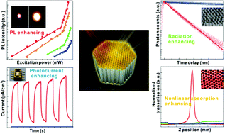
Strongly coupled plasmonic nanostructures with sub-10 nm gaps can enable intense electric field enhancements which greatly benefit the various light–matter interactions. From the point view of practical applications, such nanostructures should be of low-cost, facile fabrication and processing, large-scale with high-yield of the ultrasmall gaps, and easy for integration with other functional components. However, nowadays techniques for reliable fabrication of these nanostructures usually involve complex, time-consuming, and expensive lithography procedures, which are limited either by their low-throughput or the small areas obtained. On the other hand, so far most of the studies on the sub-10 nm gap nanostructures mainly focused on the surface-enhanced Raman scattering and high-harmonic generations, while leaving other nonlinear optical properties unexplored. In this work, using a scalable process without any lithography procedures, we demonstrated a centimeter-scale ordered plasmonic nanorod array film (PNRAF) with well-defined sub-10 nm interparticle gaps as a versatile platform for strongly enhanced light–matter interactions. Specifically, we showed that due to its plasmon-induced localized electromagnetic field enhancements, the Au PNRAF could exhibit extraordinary intrinsic multi-photon avalanche luminescence (MAPL) and nonlinear saturable absorption (SA). Furthermore, the PNRAF can be easily integrated with semiconductor quantum dots (SQDs) as well as wide bandgap semiconductors to strongly enhance their fluorescence and photocurrent response, respectively. Our method can be easily generalized to nanorod array films consisting of other plasmonic metals and even semiconductor materials, which can have multiple functionalities derived from different materials. Overall, the findings in our study have offered a potential strategy for design and fabrication of nanostructures with ultrasmall gaps for future photonic and optoelectronic applications.


 Please wait while we load your content...