
 Open Access Article
 This Open Access Article is licensed under a Creative Commons Attribution-Non Commercial 3.0 Unported Licence
Defect/oxygen assisted direct write technique for nanopatterning graphene†
Alberto
Cagliani
*a,
Niclas
Lindvall
b,
Martin Benjamin Barbour Spanget
Larsen
a,
David M. A.
Mackenzie
a,
Bjarke Sørensen
Jessen
a,
Timothy J.
Booth
a and
Peter
Bøggild
*a
aDTU Nanotech—Center for Nanostructured Graphene, Technical University of Denmark, Building 345 East, DK-2800 Kgs. Lyngby, Denmark. E-mail: Alberto.Cagliani@nanotech.dtu.dk; Peter.Boggild@nanotech.dtu.dk
bDepartment of Microtechnology and Nanoscience – Chalmers University of Technology, SE-41296 Gothenburg, Sweden
First published on 6th March 2015
Abstract
High resolution nanopatterning of graphene enables manipulation of electronic, optical and sensing properties of graphene. In this work we present a straightforward technique that does not require any lithographic mask to etch nanopatterns into graphene. The technique relies on the damaged graphene to be etched selectively in an oxygen rich environment with respect to non-damaged graphene. Sub-40 nm features were etched into graphene by selectively exposing it to a 100 keV electron beam and then etching the damaged areas away in a conventional oven. Raman spectroscopy was used to evaluate the extent of damage induced by the electron beam as well as the effects of the selective oxidative etching on the remaining graphene.
Introduction
One of the unique properties of graphene is that the electrical, chemical, optical and mechanical properties1,2 can be tuned by nanopatterning.3–8 While the literature so far has focused mainly on the creation of an energy bandgap by cutting graphene into nanoribbons3,9–11 or an antidot lattice/nanomesh,4,9,12 other properties such as a magnetic dipoles or a strong anisotropy in the transport regime have been predicted for nanopatterned graphene.13,14 As the interaction with chemical species depends strongly on the presence of defects, nanopatterning has also been used to enhance the gas sensitivity.6,7,15 Moreover, graphene nanopatterning offers the possibility of manipulating the absorption of visible and infrared light,16 as well as plasmons.17 For all these applications the critical pattern dimensions were in the sub-50 nm range, which imposes stringent requirements for the resolution of the patterning techniques to be used. So far, the most widely used lithographic techniques capable of achieving critical dimensions below 50 nm in graphene are electron beam lithography (EBL),3,18 block copolymer lithography4,9,11 and colloidal lithography.19 Despite the efforts to direct the formation of patterns by pre-deposited mechanical or chemical guides11 or external fields,20 block copolymer lithography and colloidal lithography are strongly limited in terms of the range of possible patterns that can be generated compared to beam-induced patterning.A common issue for self-assembly techniques and EBL is that they require a protective mask to be in physical contact with graphene during patterning. The process of creating the mask, or even the simple contact of the mask with graphene, will in many cases compromise the properties of graphene.21–26 A frequently used inorganic e-beam resist for sub-20 nm features in EBL is hydrogen silsesquioxane (HSQ), which is known for doping graphene and being very difficult to remove.3,21 The positive resist poly(methyl methacrylate) (PMMA) is used to a much greater extent, but under certain circumstances can lead to the presence of unwanted polymer residues, which are difficult to fully remove, and also electrically dope graphene and ultimately reduce the carrier mobility.22–24,26 Block copolymer lithography typically requires complex optimization of the lithographic process, which still prevents widespread use of such techniques in the graphene community.27–29 Several forms of direct-write techniques that do not require a mask have been proposed. Transmission Electron Microscope (TEM) has been used for nanopatterning nanoribbons in graphene, but this technique cannot be scaled up.30,31 The electron beam can also be used to change the chemical properties of graphene at the nanoscale, tuning its conductivity by up to 7 orders of magnitude, via selective defluorination of fluorinated graphene.32 Laser ablation has been used as well, but the resolution is limited to the micron range by the spot-size of the beam.33 Thiele et al.34 recently demonstrated the possibility of etching graphene with an e-beam combined with an oxygen rich atmosphere using an Environmental Scanning Electron Microscope (ESEM). Unfortunately, E-SEMs are not widely available, are costly and are not suitable for large-area patterning.
Therefore, there is still a strong demand of a patterning technique that does not involve any contact between graphene and other materials, reaches sub-50 nm resolution, is simple and uses standard equipment found in cleanrooms. In this work we consider an approach to pattern graphene with sub-40 nm features, which does not require polymers or solvents, and also does not require an environmental SEM for introduction of reactive species,34 but just an e-beam writer and an oven operating in air at atmospheric pressure. It is based on a two-step process, where the graphene is selectively highly damaged by the electron beam that defines the patterned areas, which are then removed in an oxygen rich atmosphere at 435 °C. The possibility of damaging graphene using an electron beam has been previously investigated,36–38 demonstrating the possibility of controlled modifications of the graphene properties.
Results and discussion
In Fig. 1a the two-step direct write nanopatterning process is illustrated. Graphene was produced via exfoliation of natural graphite on silicon wafers with a 100 nm silicon dioxide coating. Identification and location of single layer graphene areas were done by the automated spectrally resolved optical microscopy system introduced in ref. 35. A JEOL-9300FS EBL system was used to irradiate the sample. While the relatively high acceleration voltage of 100 kV leads to a smaller interaction cross-section compared to scanning electron microscopes, it is just above the threshold for knock-on damage of freestanding single layer graphene, reported to be around 85 keV by several authors.39,40 Raman spectroscopy was used to quantify the lattice defect density induced by the irradiation. The ratio I(D)/I(G) of the main defect-activated D-peak intensity at ∼1320 cm−1 divided by the G peak intensity indicates the degree of amorphization of the irradiated graphene as a function of the electron beam dose.41,42 In Fig. 1b the I(D)/I(G) increases as the irradiation dose is changed from 0.185 C cm−2 to 0.7 C cm−2, showing the expected increase of defect density with dose. The trend has been reported previously for supported single and bilayer graphene.36 Cançado et al.42 showed that the characteristic length LD (average separation between defects) can be estimated by LD2 [nm2] = 1.8 × 10⁻⁹λ4 [I(D)/I(G)]−1, for LD > 10 nm. For the lowest dose tested the defect density is already LD ∼ 11.5 nm, which indicates that graphene is at the beginning of the stage I of the amorphization trajectory from pristine to nanocrystalline structure following the terminology of ref. 41. For doses between 0.7 C cm−2 and 3 C cm−2 the ratio decreases due to the high density of defects with LD being a few nanometers, as the number of intact carbon hexagons decreases. In this range the nanocrystalline structure is turned into an amorphous structure with increasing sp3 content, corresponding to the stage II of the amorphization trajectory.41,42 For higher doses the ratio is influenced by the e-beam induced deposition of amorphous carbon on the irradiated areas. Amorphous carbon deposition is a well-known phenomenon in scanning electron microscopy, where much higher doses than conventional EBL are used for imaging.43 The doses of 10–20 C cm−2 used in this work are at least three orders of magnitude higher that typical doses for high resolution EBL resist.44 Amorphous carbon affects both the G band and D band by broadening the peaks, in addition an increase of the I(D)/I(G) ratio for doses higher than 6 C cm−2 is observed, while the damage in the graphene is actually increasing, as discussed below. The presence of amorphous carbon is also indicated by the AFM images in Fig. 1S,† where the written areas show a 0.5 to 1 nm protrusion from the graphene plane as well as the presence of ridges, which match the division into polygons by the JEOL JBX9300 e-beam writer. Finally, the presence of amorphous carbon after the exposure with the e-beam of the structures is visible in the optical image in Fig. 2(a). | ||
| Fig. 1 (a) Two-step direct write nanopatterning. The graphene is directly exposed using an EBL system. The e-beam induces defects in the crystal lattice of the written areas. Graphene is then baked in air at 435 °C for 12–18 minutes to etch selectively the damaged areas. (b) Raman spectroscopy data showing the ratio of the D-peak intensity to the G-peak intensity used as an indicator of the level of lattice damage induced by the electron beam in the direct written areas. | ||
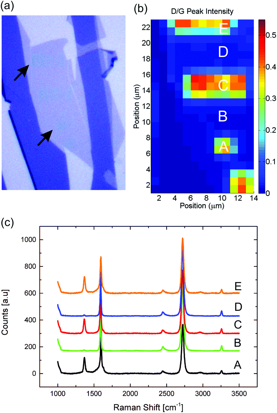 | ||
| Fig. 2 (a) Optical image of a single layer graphene after line and dot nanopatterns have been written (Dose = 12 C cm−2). The blue colouring (marked with arrows) are thought to be caused by amorphous carbon deposited during irradiation. (b) Raman spectroscopic map of the I(D)/I(G) ratio. (c) Raman spectra recorded at different spots on the sample. Within the spatial resolution of the 455 nm laser used for Raman spectroscopy, the D-peak intensity is not observed to increase outside the written areas. | ||
The spatial selectivity of the damage with respect to patterned and non-patterned regions has been investigated by micro-Raman spectroscopic mapping. A Raman map of arrays of lines and arrays of dots written in graphene is shown in Fig. 2b. The Raman spectra recorded in the written areas have a clear D peak with a corresponding I(D)/I(G) of the order of 0.4, whereas the I(D)/I(G) ratio recorded in between the exposed areas in the range 0 to 0.01 indicates that the graphene lattice is not damaged outside the written areas. The spatial map resolution is limited by the spot size (FWHM) of the 455 nm laser when used with 100× objective (∼0.5 μm), implying that the damage level can be assessed at a distance of approximately 1 μm from any written area.
In order to etch our structures, we rely on the fact that disorder in the carbon lattice generally promotes the chemical etch rate in any aggressive environment, including oxidative conditions.45,46 The same principle has been used extensively for purification of carbon nanotubes (CNT), where the much higher resistance to oxygen etching of sp2 carbon compared to amorphous carbon eliminates residual soot and defected nanotubes from the synthesis products.45,46 The oxygen etching of graphite and pristine exfoliated graphene has been studied both experimentally47,48 and theoretically.49,50 The etching proceeds radially from defects, whether these are created intentionally or are already present.47,50 This is to be expected since the basal plane of graphene is much less reactive than vacancies.50 In our work, the selective etching of damaged areas is performed in a conventional oven using air at atmospheric pressure. A temperature of 435 °C was optimal in terms of removing patterned graphene in a reasonable time frame, while still being able to keep etching of the non-patterned regions to a minimum. At 440 °C the etching proceeded significantly faster, making the etching step difficult to control and at 450 °C unexposed graphene flakes were etched after few minutes. This strong dependence on the reactivity with oxygen of graphene is also observed in literature.47,48 In Fig. 3 the etching of areas written with different doses is shown using optical, SEM images and Raman maps of the I(D)/I(G) ratio and intensity of the 2D peak. The written areas are squares of 4 by 4 microns and appear after irradiation as blue halos under the optical microscope (marked with arrows in Fig. 3c), while they appear as dark squares under the scanning electron microscope (SEM), due to charging of the SiO2 by the electron beam (Fig. 3a). After 6 minutes of etching, the bluish squares disappeared. We attribute this to the removal of the thin layer of amorphous carbon nearly always deposited during the e-beam irradiation and imaging.43 After 12 minutes the etching of graphene is clearly visible (see Fig. 3c). After 16 minutes the squares exposed with doses of 7 C cm−2 and 10 C cm−2 retain less than 3% of the initial contrast of graphene on the SiO2 (see Fig. 2S†). The micro-Raman map in Fig. 3d also indicates that the graphene has been largely removed within the squares, as the 2D peak intensity at the center of the squares is more than 20 times smaller than in non-exposed areas (after 16 minutes of etching). In Fig. 4, the SEM images of the squares with doses 10 C cm−2 and 5 C cm−2 are shown. After 6 minutes of etching no change is visible in agreement with the optical images in Fig. 3c. After 12 minutes of etching the 10 C cm−2 square is almost fully etched, while ∼80% of the graphene is still present for the 5 C cm−2 square. After 16 minutes the 10 C cm−2 square is fully clear of graphene, whereas the 5 C cm−2 still show signs of graphene at the edges.
 | ||
| Fig. 3 (a) Scanning Electron Micrograph of a single graphene layer after direct write (DW). Dark squares appears where the e-beam exposed areas. (b) I(D)/I(G) ratio Raman map after DW. Areas with no G-peak are set to white. (c) Optical images: blue squares appearing after e-beam are thought to be electron beam induced amorphous carbon, which are removed after 6 minutes at 435 °C in air; after 12 minutes the etching is partially completed; after 16 minutes the etching is completed for all squares. (d) I(2D) intensity Raman map in arbitrary units recorded after etching. | ||
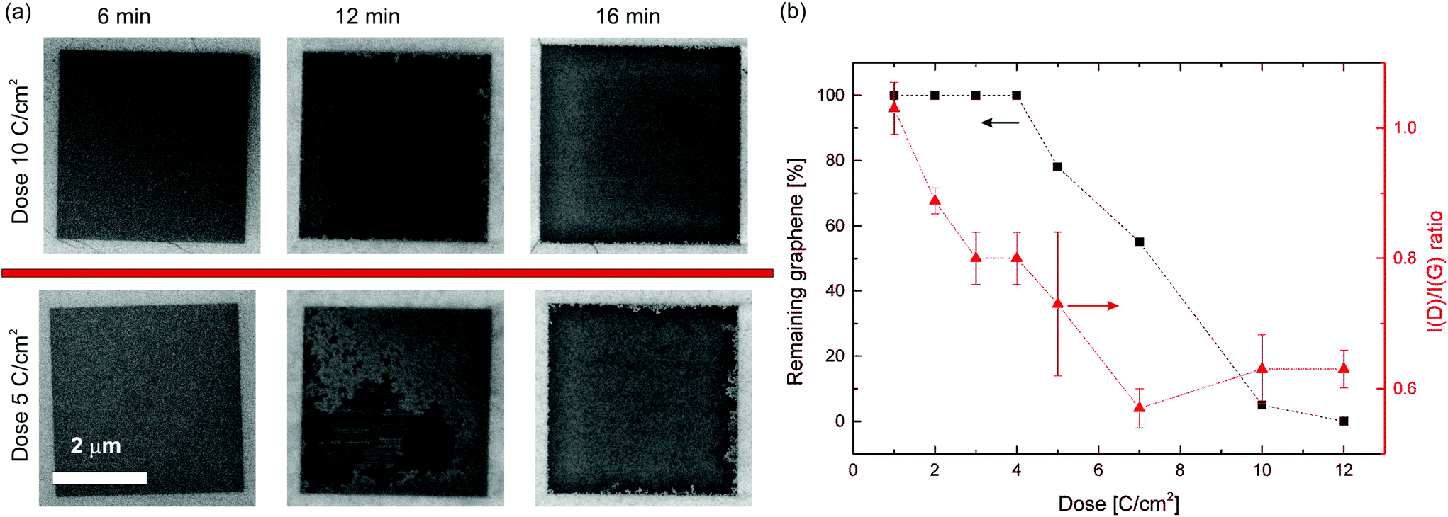 | ||
| Fig. 4 (a) Scanning Electron Microscope (SEM) images illustrating how the etching depends on time and dose for 4 × 4 μm exposed areas. After 6 minutes no etching can be seen. After 12 minutes the square with dose of 10 C cm−2 is almost complete (∼97% etched), while the 5 C cm−2 square still presents a large amount of graphene (∼20% etched). After 16 minutes the upper square is fully etched, whereas the lower square still present some remaining material at the edges. (b) The remaining graphene after 12 minutes of oxidative etching is plotted as a function of the direct write dose (black squares); on the right axis the I(D)/I(G) ratio is reported (red triangles). | ||
In order to study the correlation between electron dose and graphene etch rate, the percentage of remaining graphene after 12 minutes is plotted against the dose in Fig. 4b, showing the expected correlation between dose and removed graphene. The higher defect density permits the etching to start from more defects at the same time, leading to an earlier complete removal. While the I(D)/I(G) ratio is higher for 10 and 12 C cm−2 than for 7 C cm−2, the etching speed indicates that the defect density increases with the dose. The etching results of two other samples are shown in Fig. 3S.† For all samples a similar relation between dose, damage and etching speed is observed. The time required to fully remove the graphene (clearing time) varied across all samples between 12 and 16 minutes for 12 C cm−2, and 12 and 18 minutes for 5 C cm−2. The estimation of the clearing time is difficult because the samples could not be examined by SEM at sufficiently short intervals of etching time due to the risk of introducing measurement bias from unwanted electron beam induced damage and carbon deposition. Moreover, the etching rate increases as the etching proceeds due to the increase of free edges and vacancies, which in turn leads to acceleration of the removal of carbon atoms. Below a dose of 5 C cm−2, the removal was not completed even after 20 minutes etching time. In order to minimize the exposure to the electron beam of the SEM during the imaging of such samples, care was taken to acquire the images as single scans with a high scan rate.
In order to test the lithographic resolution, critical features in the 20–200 nm range were written by patterning lines and hole arrays. In Fig. 5 lines written with 12 C cm−2 and etched at 435 °C for 16 minutes are clearly visible. The minimum line width with complete etching is 37 ± 2 nm. Compared to the design a systematic enlargement of the line width at 12 C cm−2 is observed, but the standard deviation of the line width is less than 5% for all lines (see Fig. 5c). The same pattern was also written at 7 C cm−2 on the same graphene flake, but in this case the thinnest line with complete etch was 33 nm wide, with a standard deviation of 27%. As expected 12 C cm−2 dose lead to wider lines, while 7 C cm−2 pattern had consistently higher standard deviations as a consequence of increased edge roughness. Finally, 20 nm designed lines were clearly etched when separated by 160 nm, but not resolved when separated by 80 nm or less (last 2 arrays on the left of Fig. 5). Square arrays of nanometer sized holes were also realized (see ESI, Fig. S4†). The smallest resolved pitch (center-to-center distance) and hole diameter were 100 nm pitch with 40 ± 7 nm in diameter. We could not resolve arrays of holes with a pitch lower than 100 nm.
 | ||
| Fig. 5 (a) SEM image of direct written lines at 12 C cm−2 and etched at 435 °C for 16 minutes. (b) High magnification SEM image of the 37 nm lines etched into single layer graphene. (c) Correlation between designed and measured line width after etching for 16 minutes at 435 °C. 2D etching simulation of the etching sequence for two different initial defect densities. (d) 2D etching simulation of the etching sequence for two different initial defect densities. | ||
Simulations of the patterning process were used to visualize the lithography process. The sample space is divided in a 50 by 200 square mesh where each element represents a 1 nm2 region of the graphene flake. The irradiation damage caused by the electron exposure is simulated by an initial removal of a certain number of elements distributed evenly within the pattern region with a tunable average distance <LD>. The accelerated oxidation of already damaged graphene during the etching is simulated by sequentially removing the nearest neighbor elements of a defect at each iteration. The edge roughness of the etched line upon completion of the etching depends strongly on the initial number of defects, i.e. the effective dose in the experiments (see Fig. 5S†). By comparing the edge roughness of the SEM images with the edge roughness generated by the simulations the initial defect densities for the 12 C cm−2 is estimated to be <LD> = 1.8 nm and for the 7 C cm−2 is <LD> = 3.6 nm. These values qualitatively agree with the analysis of the ratio evolution in Fig. 1b.
Finally, the damage of the crystal lattice of graphene after etching in the unpatterned areas was investigated by recording the I(D)/I(G) ratio of etched samples. As seen in Fig. 6 the I(D)/I(G) ratio is higher where the nanopattern was etched, which could be explained by presence of the new edges. Moreover, the ratio also increases rather uniformly across the all flake with an average value of 0.25 outside the written areas. A similar value was measured for graphene flakes that were not patterned, but exposed to atmospheric air at 435 °C for 16 minutes. This leads us to conclude that irradiated areas do not necessarily lead to generation of extra defects in the nearby pristine areas during the etching. We suggest that the generation of defects in the pristine areas is instead due to the creation of vacancies and distortion of the basal plane due to chemical bonding of oxygen complex to the carbon atoms.47 However, it should be noticed that a I(D)/I(G) ratio of 0.25 corresponds to a LD of ∼18 nm. While linear defects separated by 18 nm, such as is the case for lithographically defined nanoribbons, have a significant impact on transport properties, point-like defects with similar separation were found by Liu et al.38 to result in just 20% reduction of carrier mobility. A similar conclusion was achieved by Buchowicz et al.51 Finally, the exposure to air at 435 °C leaves the graphene p-doped.47 This is supported by our data by the shift of the G peak in the range 1598–1602 cm−1 and the decrease of the FWHM of the G peak. On the other hand it has been shown that the doping can be substantially reduced by several techniques, such as exposing to a UV lamp in an inert atmosphere52 or annealing in an inert gas.52
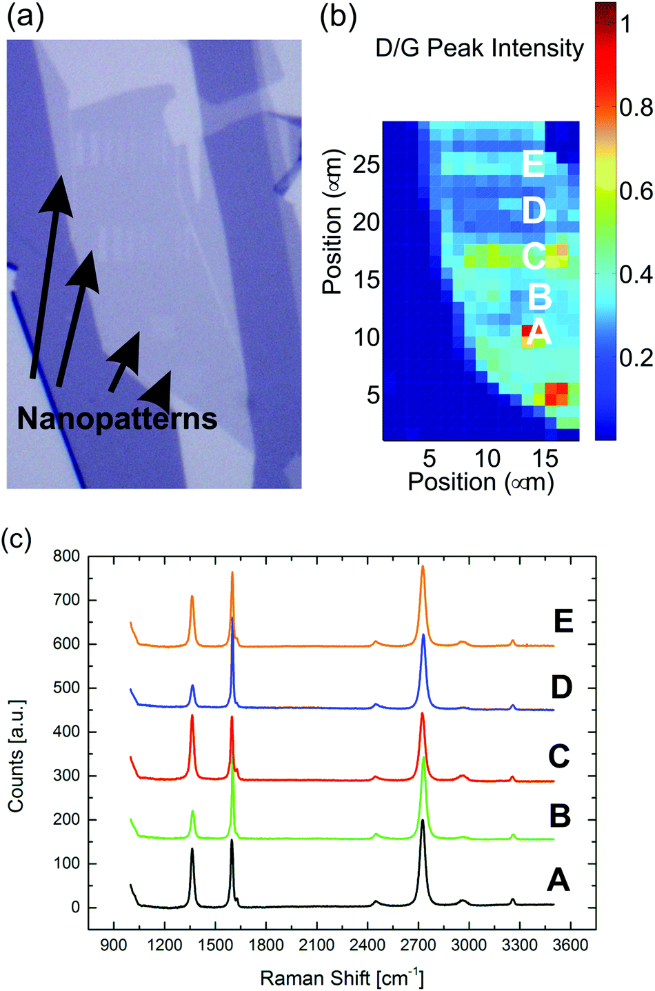 | ||
| Fig. 6 (a) Optical image of a single layer graphene after nanopatterns have been etched. (b) Raman map of the I(D)/I(G) ratio. (c) Raman spectra at different spots on the sample. | ||
Conclusions
In conclusion, we have presented a straightforward, rapid nanopatterning route that does not involve any masking material, polymer contact or solvents, and allow sub 40 nm structures to be defined directly in graphene. This can be done without introduction of gases in the lithographic system, permitting dedicated electron beam writers to be used rather than inferior environmental electron microscopes. The direct write approach comprises of just two steps: damaging the graphene in the areas to be removed by high dose e-beam exposure and the oxidative selective etch of graphene patterns in a conventional oven. While the resolution has not yet been shown comparable to state-of-the-art conventional electron beam lithography, it is reasonable to believe that further optimization should lead to even better resolution and control of the doping.Experimental details
Single layer graphene was exfoliated on 100 nm SiO2 from natural graphite and identified by optical contrast using an automated identification system and Raman spectroscopy. A Thermo DXR-Raman system with a laser wavelength of 455 nm was used for mapping of the graphene samples. The e-beam lithography system (EBL) was a JEOL-9300FS operating at 100 kV with beam currents of either 1 or 10 nA. For etching a programmable Heraeus oven with a range up to 1000 degrees was used. A SEM Zeiss Supra operating at 5 kV acceleration voltage was used to image the samples (secondary electron detector).Acknowledgements
The authors wish to thank the Center for Nano-structured Graphene and the European Project NMP-FP7 Grafol for financial support. The Center for Nanostructured Graphene (CNG) is sponsored by the Danish National Research Foundation, Project DNRF58. The authors would like to thank MCI2 personnel at Chalmers University for helping during the EBL exposures. T.B. gratefully acknowledges support from the Danish Council for Independent Research, Technology and Productions Sciences grant GraVOX. The authors thank EC Graphene FET Flagship, contract number 604391.Notes and references
- A. K. Geim, Science, 2009, 324, 1530–1534 CrossRef CAS PubMed.
- A. H. Castro Neto, N. M. R. Peres, K. S. Novoselov and a. K. Geim, Rev. Mod. Phys., 2009, 81, 109–162 CrossRef CAS.
- M. Han, B. Özyilmaz, Y. Zhang and P. Kim, Phys. Rev. Lett., 2007, 98, 206805 CrossRef.
- J. Bai, X. Zhong, S. Jiang, Y. Huang and X. Duan, Nat. Nanotechnol., 2010, 5, 190–194 CrossRef CAS PubMed.
- J. Feng, W. Li, X. Qian, J. Qi, L. Qi and J. Li, Nanoscale, 2012, 4, 4883–4899 RSC.
- R. K. Paul, S. Badhulika, N. M. Saucedo and A. Mulchandani, Anal. Chem., 2012, 84, 8171–8178 CrossRef CAS PubMed.
- A. Cagliani, D. M. A. Mackenzie, L. K. Tschammer, F. Pizzocchero, K. Almdal and P. Bøggild, Nano Res., 2014, 7, 743–754 CrossRef CAS.
- M. Dvorak, W. Oswald and Z. Wu, Sci. Rep., 2013, 3, 2289 Search PubMed.
- M. Kim, N. S. Safron, E. Han, M. S. Arnold and P. Gopalan, ACS Nano, 2012, 6, 9846–9854 CrossRef CAS.
- X. Li, X. Wang, L. Zhang, S. Lee and H. Dai, Science, 2008, 319, 1229–1232 CrossRef CAS PubMed.
- J. G. Son, M. Son, K.-J. Moon, B. H. Lee, J.-M. Myoung, M. S. Strano, M.-H. Ham and C. a. Ross, Adv. Mater., 2013, 25, 4723–4728 CrossRef CAS PubMed.
- X. Liang, Y.-S. Jung, S. Wu, A. Ismach, D. L. Olynick, S. Cabrini and J. Bokor, Nano Lett., 2010, 10, 2454–2460 CrossRef CAS PubMed.
- H.-X. Yang, M. Chshiev, D. W. Boukhvalov, X. Waintal and S. Roche, Phys. Rev. B: Condens. Matter, 2011, 84, 214404 CrossRef.
- J. G. Pedersen, A. W. Cummings and S. Roche, Phys. Rev. B: Condens. Matter, 2014, 89, 165401 CrossRef.
- L. K. Randeniya, H. Shi, A. S. Barnard, J. Fang, P. J. Martin and K. K. Ostrikov, Small, 2013, 9, 3993–3999 CrossRef CAS PubMed.
- Z. Fang, Y. Wang, A. E. Schlather, Z. Liu, P. M. Ajayan, F. J. G. de Abajo, P. Nordlander, X. Zhu and N. J. Halas, Nano Lett., 2014, 14, 299–304 CrossRef CAS PubMed.
- F. J. García de Abajo, ACS Photonics, 2014, 1, 135–152 CrossRef.
- A. Giesbers, E. Peters, M. Burghard and K. Kern, Phys. Rev. B: Condens. Matter, 2012, 86, 8–10 CrossRef.
- A. Sinitskii and J. M. Tour, J. Am. Chem. Soc., 2010, 132, 14730–14732 CrossRef CAS PubMed.
- D. J. C. Herr, J. Mater. Res., 2011, 26, 122–139 CrossRef CAS.
- K. Brenner and R. Murali, Appl. Phys. Lett., 2010, 96, 063104 CrossRef PubMed.
- Y.-C. Lin, C.-C. Lu, C.-H. Yeh, C. Jin, K. Suenaga and P.-W. Chiu, Nano Lett., 2012, 12, 414–419 CrossRef CAS PubMed.
- G. Yu, X. Liu, G. Xing, S. Chen, C. F. Ng, X. Wu, E. K. L. Yeow, W. S. Lew and T. C. Sum, J. Phys. Chem. C, 2014, 118, 708–713 CAS.
- L. Gammelgaard, J. M. Caridad, A. Cagliani, D. M. a. Mackenzie, D. H. Petersen, T. J. Booth and P. Bøggild, 2D Mater., 2014, 1, 035005 CrossRef.
- N. Petrone, I. Meric, J. Hone and K. L. Shepard, Nano Lett., 2012, 2–6 Search PubMed.
- A. Pirkle, J. Chan, A. Venugopal, D. Hinojos, C. W. Magnuson, S. McDonnell, L. Colombo, E. M. Vogel, R. S. Ruoff and R. M. Wallace, Appl. Phys. Lett., 2011, 99, 122108 CrossRef PubMed.
- E. Han, K. O. Stuen, Y. La, P. F. Nealey and P. Gopalan, Macromolecules, 2008, 41, 9090–9097 CrossRef CAS.
- K. W. Guarini, C. T. Black, K. R. Milkove and R. L. Sandstrom, J. Vac. Sci. Technol., B: Microelectron. Nanometer Struct.–Process., Meas., Phenom., 2001, 19, 2784 CrossRef CAS.
- E. Han, K. O. Stuen, M. Leolukman, C.-C. Liu, P. F. Nealey and P. Gopalan, Macromolecules, 2009, 42, 4896–4901 CrossRef CAS.
- F. Börrnert, L. Fu, S. Gorantla, M. Knupfer, B. Büchner and M. H. Rümmeli, ACS Nano, 2012, 6, 10327–10334 CrossRef PubMed.
- Q. Xu, M.-Y. Wu, G. F. Schneider, L. Houben, S. K. Malladi, C. Dekker, E. Yucelen, R. E. Dunin-Borkowski and H. W. Zandbergen, ACS Nano, 2013, 7, 1566–1572 CrossRef CAS PubMed.
- F. Withers, T. H. Bointon, M. Dubois, S. Russo and M. F. Craciun, Nano Lett., 2011, 11, 3912–3916 CrossRef CAS PubMed.
- M. F. El-Kady and R. B. Kaner, ACS Nano, 2014, 8, 8725–8729 CrossRef CAS PubMed.
- C. Thiele, A. Felten, T. J. Echtermeyer, A. C. Ferrari, C. Casiraghi, H. v. Löhneysen and R. Krupke, Carbon, 2013, 64, 84–91 CrossRef CAS PubMed.
- J. D. Buron, F. Pizzocchero, B. S. Jessen, T. J. Booth, P. F. Nielsen, O. Hansen, M. Hilke, E. Whiteway, P. U. Jepsen, P. Bøggild and D. H. Petersen, Nano Lett., 2014, 14, 6348–6355 CrossRef CAS PubMed.
- D. Teweldebrhan and A. A. Balandin, Appl. Phys. Lett., 2009, 94, 013101 CrossRef PubMed.
- M. Zahid Hossain, S. Rumyantsev, M. S. Shur and A. A. Balandin, Appl. Phys. Lett., 2013, 102, 153512 CrossRef PubMed.
- G. Liu, S. Member, D. Teweldebrhan, A. A. Balandin and S. Member, IEEE Trans. Nanotechnol., 2011, 10, 865–870 CrossRef.
- C. O. Girit, J. C. Meyer, R. Erni, M. D. Rossell, C. Kisielowski, L. Yang, C.-H. Park, M. F. Crommie, M. L. Cohen, S. G. Louie and A. Zettl, Science, 2009, 323, 1705–1708 CrossRef CAS PubMed.
- J. C. Meyer, F. Eder, S. Kurasch, V. Skakalova, J. Kotakoski, H. J. Park, S. Roth, A. Chuvilin, S. Eyhusen, G. Benner, A. V. Krasheninnikov and U. Kaiser, Phys. Rev. Lett., 2012, 108, 196102 CrossRef.
- A. Ferrari and J. Robertson, Phys. Rev. B: Condens. Matter, 2000, 61, 14095–14107 CrossRef CAS.
- L. G. Cançado, a. Jorio, E. H. M. Ferreira, F. Stavale, C. a. Achete, R. B. Capaz, M. V. O. Moutinho, a. Lombardo, T. S. Kulmala and a. C. Ferrari, Nano Lett., 2011, 11, 3190–3196 CrossRef PubMed.
- R. F. Egerton, P. Li and M. Malac, Micron, 2004, 35, 399–409 CrossRef CAS PubMed.
- A. E. Grigorescu and C. W. Hagen, Nanotechnology, 2009, 20, 292001 CrossRef CAS PubMed.
- I. K. K. Hernadi, A. Siska, L. Thien-Nga and L. Forró, Solid State Ionics, 2001, 141–142, 203–209 CrossRef.
- K. Morishita and T. Takarada, J. Mater. Sci., 1999, 34, 1169–1174 CrossRef CAS.
- L. Liu, S. Ryu, M. R. Tomasik, E. Stolyarova, N. Jung, M. S. Hybertsen, M. L. Steigerwald, L. E. Brus and G. W. Flynn, Nano Lett., 2008, 8, 1965–1970 CrossRef CAS PubMed.
- H. Y. Nan, Z. H. Ni, J. Wang, Z. Zafar, Z. X. Shi and Y. Y. Wang, J. Raman Spectrosc., 2013, 44, 1018–1021 CrossRef CAS.
- J. Carlsson, F. Hanke, S. Linic and M. Scheffler, Phys. Rev. Lett., 2009, 102, 166104 CrossRef.
- S. M. Lee, Y. H. Lee, Y. G. Hwang, J. R. Hahn and H. Kang, Phys. Rev. Lett., 1999, 82, 217–220 Search PubMed.
- G. Buchowicz, P. R. Stone, J. T. Robinson, C. D. Cress, J. W. Beeman and O. D. Dubon, Appl. Phys. Lett., 2011, 98, 032102 CrossRef PubMed.
- S. Ryu, L. Liu, S. Berciaud, Y. Yu, H. Liu, P. Kim, G. W. Flynn and L. E. Brus, Nano Lett., 2010, 10, 4944–4951 Search PubMed.
Footnote |
| † Electronic supplementary information (ESI) available: The Supplementary information provided include further analysis of the optical images, topography of the samples after irradiation, SEM imaging of the etching of graphene and simulations of the etching process. See DOI: 10.1039/c4nr07585d |
| This journal is © The Royal Society of Chemistry 2015 |