
Differentiating surface and bulk interactions in nanoplasmonic interferometric sensor arrays†
Beibei
Zeng
*,
Yongkang
Gao
and
Filbert J.
Bartoli
*
Electrical and Computer Engineering Department, Lehigh University, Bethlehem, PA 18015, USA. E-mail: bez210@lehigh.edu; fjb205@lehigh.edu
First published on 3rd November 2014
Abstract
Detecting specific target analytes and differentiating them from interfering background effects is a crucial but challenging task in complex multi-component solutions commonly encountered in environmental, chemical, biological, and medical sensing applications. Here we present a simple nanoplasmonic interferometric sensor platform that can differentiate the adsorption of a thin protein layer on the sensor surface (surface effects) from bulk refractive index changes (interfering background effects) at a single sensing spot, exploiting the different penetration depths of multiple propagating surface plasmon polaritons excited in the ring–hole nanoplasmonic sensors. A monolayer of bovine serum albumin (BSA) molecules with an effective thickness of 1.91 nm is detected and differentiated from a 10−3 change in refractive index unit for the bulk solution. The noise level of the retrieved real-time sensor output compares favorably with that of traditional prism-based surface plasmon resonance sensors, but is achieved using a significantly simpler collinear transmission geometry and a miniaturized sensor footprint.
1. Introduction
Surface plasmon resonance (SPR) biosensors have unquestionable advantages for studying biological and chemical interactions, and have become the gold standard for real-time, label-free detection of biomolecular interactions.1–9 However, it remains a challenge for SPR sensors to detect small concentrations of target analytes in complex solutions.10 Several approaches have been proposed to differentiate target surface biomolecular binding from background interference effects such as non-specific adsorption and bulk refractive index (RI) variations. A two-plasmon spectroscopic approach was employed to excite two SPR modes with different penetration depths at two different locations on the sensor surface.11–13 Another approach proposed a two-channel-SPR compensation technique using two separated sensor channels, one without surface functionalization and the other covered by surface receptors with an affinity for specific analytes.14 Although these two methods have successfully retrieved and differentiated surface and background changes, identical conditions cannot be guaranteed at two different sensing spots, and an increased number of sensor channels is required. Subsequently, a third approach was proposed utilizing self-referencing dual-mode SPR sensors, in which a broadband light source illuminates a single sensing spot and simultaneously excites two distinct SPR modes with different penetration depths (e.g. long- and short-range SPRs,10,15 or two SPR-waveguide resonances under dual polarizations16). Generally, all of the above approaches are restricted to the traditional prism-based SPR configuration,3 which, while successful for numerous applications, suffers from the low achievable spatial resolution and throughput, as well as its complex and bulky optical geometry.Nanoplasmonic biosensors are being actively investigated for next-generation sensing applications that require system miniaturization, simpler optical geometry, increased spatial resolution, and high-throughput multiplexing detection.17–27 Nanoplasmonic biosensors frequently employ metallic nanoparticles, nanogratings, and nanohole arrays to couple incident light directly to surface plasmon polaritons (SPPs),17–26 utilizing a much simpler collinear optical configuration. This offers significant system miniaturization and integration. These nanoplasmonic biosensor arrays allow high-throughput multiplexed detection, when using a CCD camera for simultaneous measurement of the transmitted light intensity from multiple sensing spots, and can achieve a high spatial resolution, with sensing spot size as small as a few μm2.19 However, their performance is generally limited by their broad spectral line-width, low contrast and weak resonance intensity.17–25 The reported detection limits for multiplexed detection in these nanoplasmonic biosensors are typically one to two orders of magnitude poorer than that of commercial SPR systems.17–25 To overcome this limitation, nanoplasmonic interferometric biosensors were recently proposed, and shown to exhibit interference patterns with narrow linewidths and high contrast ratios, significantly improving the detection resolution. These nanoplasmonic interferometric biosensors utilize phase-sensitive interferences between the free-space light and propagating SPPs to achieve superior spatial resolution and detection performance.28–30 Using circular nanoplasmonic interferometer arrays, our group has recently demonstrated a spectral detection resolution of 0.4 pg mm−2, comparable to state-of-the-art commercial SPR sensors, but that was achieved using a much simpler collinear transmission geometry and a miniaturized sensor footprint.29 In addition, a record high sensing figure-of-merit of 146 (FOM* = (dI/I0)/dn) can be obtained for these nanoplasmonic interferometric sensors using intensity-interrogation CCD imaging techniques. These are quite promising for scalable high-throughput multiplexing applications.
Until now, there has been a notable absence of efforts to differentiate surface biomolecular binding from interfering background effects in nanoplasmonic biosensors. This can be attributed in part to the difficulty in exciting and detecting multiple SPPs with significantly different penetration depths in a single sensing spot for metallic nanoparticle and nanoaperture array sensors.17–22 In contrast, nanoplasmonic interferometric biosensors support multiple propagating SPPs with different penetration depths on the same sensing spot.29 In the present work, we have expanded the functionality of the promising circular nanoplasmonic interferometric sensing platform and have demonstrated a new self-referenced nanoplasmonic biosensor. By exploiting the different penetration depths of multiple propagating SPPs excited within the ring–hole nanostructures, surface biomolecular binding can be differentiated from bulk RI changes within a single sensing spot. A monolayer of BSA molecules with an effective thickness of 1.91 nm and a background change of 10−3 refractive index units (RIU) are both successfully detected and differentiated, with a low noise level that is comparable with that obtained for the traditional prism-based SPR sensors.10
2. Results and discussion
A schematic of the collinear transmission setup is shown in Fig. 1(a). A beam of white light from a 100 W halogen lamp illuminated the sensor chip through the condenser of an Olympus IX81 inverted microscope. The field and aperture diaphragms of the condenser were both closed to obtain a nearly collimated light beam. The transmitted light was collected by a 40× objective lens (numerical aperture, NA = 0.6), which was coupled to an Ocean Optics USB4000 portable spectrometer for spectral measurements. An Indel E-beam evaporation system was used to deposit 5 nm thick titanium and subsequently a 300 nm thick Au film onto a pre-cleaned standard Fisher Scientific glass slide. FEI Scios Dual-Beam focused ion beam (FIB) milling (Ga+ ions, 30 kV, 30 pA) was used to fabricate arrays of ring–hole nanostructures with a center-to-center distance of 12.5 μm on the Au film, as shown in Fig. 1(b). A 12 × 12 ring–hole interferometer array thus has a sensor footprint of around 150 × 150 μm2. The structural parameters for each ring–hole nanostructure are the same as those reported in ref. 29 (Fig. S1 in ESI†). After the FIB milling, the sensor chip was cleaned using oxygen plasma (PX-250, March Instruments) and bonded to a PDMS microfluidic channel, as shown in Fig. 1(c). The PDMS microfluidic channels were fabricated by conventional soft lithography. A SU8-50 (Microchem) master mold of the channel (50 μm deep and 4 mm wide) was patterned on a silicon wafer by photolithography. A 10![[thin space (1/6-em)]](https://www.rsc.org/images/entities/char_2009.gif) :1 ratio of PDMS (Sylgard 184, Dow corning) and a curing agent were used to cast the mold, which was then baked at 70 °C for 3 hours. The PDMS channel was cut and peeled from the master, and then inlet and outlet holes were punched for the tubing. The multiple circular grooves scatter the normally incident broadband light into SPPs that propagate towards the central nanohole. The groove periodicity was carefully chosen so that the SPPs launched at each groove are approximately in phase in the spectral region of interest, generating strong propagating SPP waves directed towards the central nanohole. The red solid curve shown in Fig. 1(d) is the measured transmission spectrum of the 12 × 12 ring–hole interferometer array in a water environment. The multiple transmission peaks and valleys result from the constructive and destructive interference between propagating SPPs and the light transmitted directly through the central nanoholes.29 The spectral positions of these interference peaks and valleys (e.g. λ1 to λ6) are very sensitive to local RI changes, caused by either surface effects (e.g. biomolecular adsorption) or background RI changes (e.g. temperature or compositional variations).
:1 ratio of PDMS (Sylgard 184, Dow corning) and a curing agent were used to cast the mold, which was then baked at 70 °C for 3 hours. The PDMS channel was cut and peeled from the master, and then inlet and outlet holes were punched for the tubing. The multiple circular grooves scatter the normally incident broadband light into SPPs that propagate towards the central nanohole. The groove periodicity was carefully chosen so that the SPPs launched at each groove are approximately in phase in the spectral region of interest, generating strong propagating SPP waves directed towards the central nanohole. The red solid curve shown in Fig. 1(d) is the measured transmission spectrum of the 12 × 12 ring–hole interferometer array in a water environment. The multiple transmission peaks and valleys result from the constructive and destructive interference between propagating SPPs and the light transmitted directly through the central nanoholes.29 The spectral positions of these interference peaks and valleys (e.g. λ1 to λ6) are very sensitive to local RI changes, caused by either surface effects (e.g. biomolecular adsorption) or background RI changes (e.g. temperature or compositional variations).
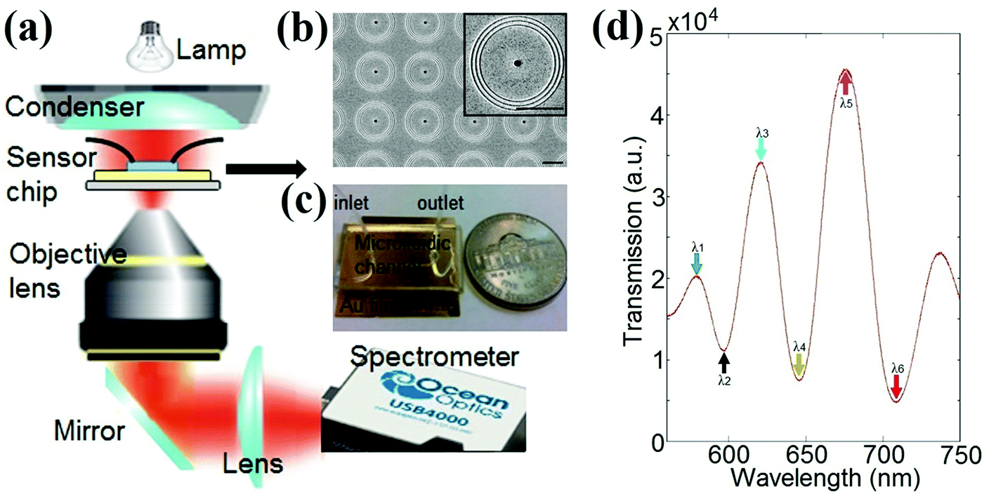 | ||
| Fig. 1 (a) Schematic of the optical setup. (b) Scanning electron microscopy (SEM) images of the fabricated interferometric ring–hole arrays. The center-to-center distance between each ring–hole nanostructure is 12.5 μm, and the sensor footprint is 150 × 150 μm2. The scale bar represents 5 μm. The inset shows an enlarged ring–hole nanostructure. (c) A photograph of the sensor chip, consisting of 12 × 12 ring–hole interferometer arrays fabricated on a 300 nm thick Au film, integrated with a PDMS microfluidic channel and inlet/outlet tubing. (d) Measured transmission spectra for the 12 × 12 ring–hole interferometer arrays. The multiple transmission peaks and valleys are marked by 6 colored arrows, corresponding to wavelengths from λ1 to λ6. | ||
SPPs excited at different wavelengths in the interferometric ring–hole nanostructures have different penetration depths δd into the surrounding aqueous medium, which are described by  , where λ is the excitation wavelength, εm and εd are the relative permittivity of the metal and dielectric medium, respectively (Fig. S2 in ESI†).31–36 SPPs with different penetration depths δd have different relative sensitivities to surface and bulk RI changes, due to differing overlaps between the electromagnetic fields of SPPs and the surrounding medium.10 Generally, SPPs with shorter excitation wavelengths have smaller δd and are more sensitive to RI changes due to biomolecular adsorption at the sensor surface. Similarly, SPPs with larger δd are more sensitive to bulk RI changes.17 Therefore, surface and bulk RI changes will generally result in different wavelength shifts for each interference peak and valley, from λ1 to λ6. This enables the separation of surface and bulk RI changes in a single sensing spot by recording the wavelength shifts of multiple peaks or valleys. This can be accomplished simply using a single spectrometer. To describe this process, we define the surface sensitivity as the shift in wavelength caused by a 1 nm change in the surface layer thickness (e.g. due to biomolecular adsorption), and the bulk RI sensitivity as the shift in wavelength due to a unit change in the bulk refractive index (e.g. using background solutions with different glycerol concentrations). The net sensor response, including contributions from both surface and bulk RI changes, is given by10,15
| Δλm = SSmΔde + SBmΔnB | (1) |
The spectral positions of each interference peak and valley (λ1 to λ6) were measured as a function of time as the sensor surface sequentially experienced a simple change in bulk RI, surface adsorption of BSA molecules, and combined changes in BSA surface coverage and bulk RI, as shown in Fig. 2(a). Deionized (DI) water was first injected into the PDMS microfluidic channel to rinse the sensor chip and define the baseline for the experiment. Subsequently, a 6% glycerol–water (6% G) solution was introduced into the channel, causing a bulk RI change of ΔnB = 0.009 RIU. Since no surface adsorption occurred during this time period, Δde = 0. Consequently, eqn (1) reduces to Δλm = SBmΔnB, and the bulk sensitivity SBm can be determined for each interference peak and valley, as shown in Fig. 2(b). Next, DI water was injected to remove the 6% G solution. A 500 μg per ml solution of BSA in water was then introduced into the channel, functionalizing the surface with a monolayer of BSA molecules. A subsequent DI water wash caused no additional wavelength shift, indicating that a saturated BSA surface monolayer had been formed with an effective thickness of Δde = 1.9 nm.37 In this case, the wavelength shift Δλm is solely due to surface binding of BSA (ΔnB = 0), and eqn (1) becomes Δλm = SSmΔde. The resulting surface sensitivity SSm was calculated for each interference peak and valley and is shown in Fig. 2(c). Finally, a 6% G solution was re-injected into the channel. The wavelength shift Δλm for each interference peak and valley, shown in Fig. 2(d), now reflects both surface layer BSA adsorption and bulk RI changes, simulating complex solutions. By incorporating the experimentally determined surface and bulk sensitivities SSm and SBm into eqn (1), we can determine the surface layer thickness and bulk RI changes, Δde and ΔnB, from the measured spectral shift in the interference pattern at two different wavelengths, as we illustrate below.
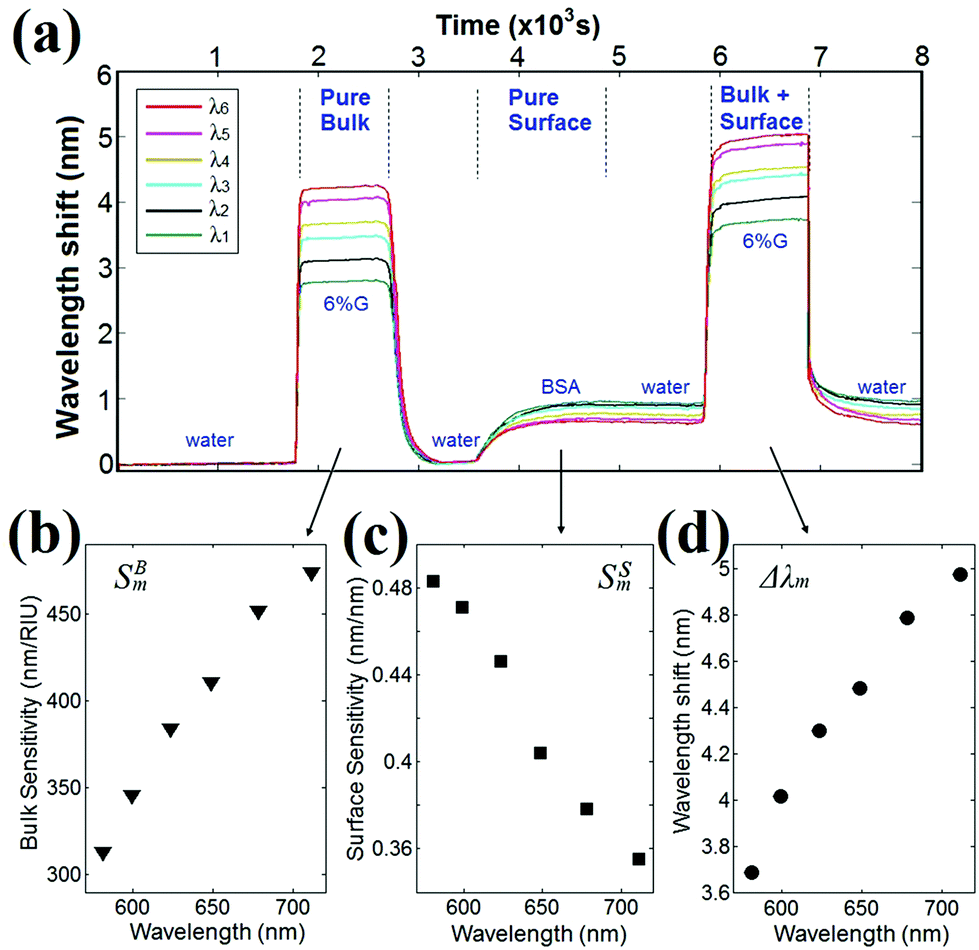 | ||
| Fig. 2 (a) Real-time sensor responses (wavelength shifts Δλm) of six different interference peaks and valleys (corresponding to wavelengths from λ1 to λ6) to changes in bulk RI (6% G) and the surface layer thickness (BSA adsorption on the sensor surface). Calibrated (b) bulk SBm and (c) surface SSm sensitivities for each interference peak and valley from λ1 to λ6. (d) Wavelength shifts Δλm of six interference peaks and valleys in complex solutions with both surface (BSA adsorption) and bulk (6% G) RI changes. | ||
To demonstrate the capability of circular nanoplasmonic interferometric sensors to differentiate surface and bulk effects in complex media, we considered an example in which the adsorption of BSA molecules on the sensor surface is detected in the presence of bulk solutions of varying refractive index. Solutions were introduced onto the sensor chip in the following order: (1) DI water, (2) 3% G, (3) 6% G, (4) DI water, (5) 500 μg per ml of BSA solution, (6) DI water, (7) 3% G, (8) 6% G, (9) DI water. The measured spectral positions of the interference minima at λ2 and λ6 are plotted in Fig. 3(a) as a function of time. Changes in the surface layer thickness Δde and bulk RI ΔnB are the two unknown quantities in eqn (1), which can be directly retrieved by straightforward mathematics. For example, variations in the surface layer thickness and bulk RI cause a shift in the spectral positions of the two interference valleys initially at λ2 = 596.7 nm and λ6 = 708.1 nm. Δλ2 and Δλ6 can be expressed as
| Δλ2 = SS2Δde + SB2ΔnB | (2) |
| Δλ6 = SS6Δde + SB6ΔnB | (3) |
 | ||
| Fig. 3 (a) Real-time sensor responses Δλ2 (black curve) and Δλ6 (red curve) to bulk RI (3% and 6% G solutions) and surface layer thickness changes (BSA adsorption) for two interference valleys at λ2 and λ6. (b) Surface layer thickness (red curve) and bulk RI (blue curve) changes retrieved using eqn (4) and (5), with calculated bulk (SB2 and SB6) and surface (SS2 and SS6) sensitivities at λ2 and λ6. The insets indicate the noise levels σS and σB (standard deviations) associated with the retrieved real-time change Δde in the surface layer thickness and the bulk RI change nB, respectively (over 20 data points). | ||
Fig. 2(b) and (c) provide the measured surface sensitivity (SS2 = 0.471 nm nm−1 and SS6 = 0.355 nm nm−1) and bulk sensitivity (SB2 = 345.8 nm per RIU and SB6 = 469.1 nm per RIU) for these two interference valleys. Eqn (2) and (3) can then be solved at each point in time for the unknown changes in the surface layer thickness Δde and bulk RI ΔnB, yielding the following expressions:
| Δde = (Δλ2/SB2 − Δλ6/SB6)/(SS2/SB2 − SS6/SB6) | (4) |
| ΔnB = (Δλ2/SS2 − Δλ6/SS6)/(SB2/SS2 − SB6/SS6) | (5) |
The resulting values of Δde and ΔnB are plotted as a function of time in Fig. 3(b). The figure shows a clear differentiation between the real-time change in the surface layer thickness Δde (red curve) and the step-like bulk RI change ΔnB (blue curve). The retrieved RI changes for the 3% and 6% G solutions, ΔnB = 0.00437 RIU and 0.00889 RIU, agree well with the values measured using a J. A. Woollam, V-VASE ellipsometer (ΔnB = 0.004 RIU and 0.009 RIU).29 The bulk RI changes in background solutions (3% and 6% G) show no influence on the retrieved change in the surface layer thickness, wherein a monolayer of BSA molecules with an effective thickness of 1.91 nm is immobilized on the sensor surface.
The uncertainty involved in extracting changes in the surface layer thickness de and bulk RI ΔnB from the real-time sensor output depends predominantly on the uncertainty in measurement of the wavelength shift (e.g. Δλ2 and Δλ6), inaccuracy of the sensor calibration (e.g. SS2,6 and SB2,6), and the difference in the wavelengths, and hence the penetration depths associated with the interference peaks and valleys employed in the extraction processes. The insets of Fig. 3(b) show the noise levels of the retrieved real-time values for Δde and ΔnB (σS = 0.009 nm and σB = 9.2 × 10⁻⁶ RIU, obtained using over 20 data points). These values are comparable to the noise levels (σS = 0.009 nm and σB = 6.9 × 10⁻⁶ RIU) reported for traditional prism-based SPR sensors.10 Note that the circular nanoplasmonic interferometric sensors utilize a significantly simpler collinear transmission geometry, a miniaturized sensor footprint, and a low-cost compact spectrometer. If more closely spaced interference peaks (valleys) were used, the difference in the penetration depths δd of the two SPP modes would be smaller, resulting in greater experimental uncertainty in differentiating the bulk and surface effects.10,15 For instance, when the adjacent interference valley at λ2 = 596.7 nm and the peak at λ3 = 621.1 nm are selected (decreasing the difference in penetration depths), the uncertainty in the extracted values of Δde and ΔnB are approximately five times larger (σS = 0.045 nm and σB = 5.5 × 10⁻⁵ RIU). While a larger wavelength separation is preferred, the noise will increase if the chosen wavelengths are beyond the optimal spectral range for interference oscillations (λ2 < λ < λ6). For the current geometry, the two interference valleys λ2 = 596.7 nm and λ6 = 708.1 nm are the optimal choice for differentiating surface and bulk effects.
3. Conclusions
A nanoplasmonic ring–hole interferometric sensor platform was shown to differentiate surface layer adsorption from interfering bulk refractive index variations based on measurements within a single sensing spot. This technique exploits the wavelength-dependent penetration depths of SPPs excited in ring–hole nanostructures, which lead to very different dependencies of surface and bulk sensitivities upon wavelength. A monolayer of BSA molecules with an effective thickness of 1.91 nm has been detected in the presence of background refractive index changes of 10−3 RIU. This sensor system utilizes a simple optical configuration, employing a collinear transmission geometry and portable spectrometer, and permits dramatically reduced sensing volumes and higher throughput assays than the traditional prism-based SPR sensors. This nanoplasmonic sensor may also be used to characterize non-specific biomolecular binding events in complex biomolecular fluidics (e.g. human serum, urine, cell cultures, etc.), and distinguish them from other background noise. It has the potential for significant impact on point-of-care diagnostics and personal healthcare applications, as well as other applications in biomedical, environmental and chemical detection.Acknowledgements
We acknowledge the financial support from the National Science Foundation (CBET-1014957).Notes and references
- J. Homola, S. S. Yee and G. Gauglitz, Sens. Actuators, B, 1999, 54, 3–15 CrossRef CAS.
- C. T. Campbell and G. Kim, Biomaterials, 2007, 28, 2380–2392 CrossRef CAS PubMed.
- J. Homola, Chem. Rev., 2008, 108, 462–493 CrossRef CAS PubMed.
- X. Fan, et al. , Anal. Chim. Acta, 2008, 620, 8–26 CrossRef CAS PubMed.
- X. Fan and I. M. White, Nat. Photonics, 2011, 5, 591 CrossRef CAS PubMed.
- X. Zhang, et al. , Opt. Express, 2011, 19, 22242 CrossRef PubMed.
- H. Zhu, et al. , Analyst, 2008, 133, 356–360 RSC.
- L. Ren, et al. , Opt. Lett., 2012, 37, 3873–3875 CrossRef.
- H. Li, et al. , J. Am. Chem. Soc., 2009, 131, 16612 CrossRef CAS PubMed.
- R. Slavík, J. Homola and H. Vaisocherová, Meas. Sci. Technol., 2006, 17, 932 CrossRef.
- J. Dostálek, H. Vaisocherová and J. Homola, Sens. Actuators, B, 2005, 108, 758 CrossRef PubMed.
- J. Homola, H. B. Lu and S. S. Yee, Electron. Lett., 1999, 35, 1105 CrossRef CAS.
- J. Homola, H. Vaisocherová, J. Dostálek and M. Piliarik, Methods, 2005, 37, 26 CrossRef CAS PubMed.
- S. Lofas, M. Malmqvist, I. Ronnberg, E. Stenberg, B. Liedberg and I. Lundstrom, Sens. Actuators, B, 1991, 5, 79 CrossRef.
- J. Guo, et al. , Opt. Lett., 2008, 33, 512 CrossRef.
- F. Bahrami, et al. , Biomed. Opt. Express, 2014, 5, 2481 CrossRef PubMed.
- A. G. Brolo, Nat. Photonics, 2012, 6, 709 CrossRef CAS.
- J. N. Anker, W. P. Hall, O. Lyandres, N. C. Shah, J. Zhao and R. P. Van Duyne, Nat. Mater., 2008, 7, 442 CrossRef CAS PubMed.
- N. C. Lindquist, A. Lesuffleur, H. Im and S.-H. Oh, Lab Chip, 2009, 9, 382 RSC.
- H. Im, J. N. Sutherland, J. A. Maynard and S.-H. Oh, Anal. Chem., 2012, 84, 1941 CrossRef CAS PubMed.
- A. A. Yanik, et al. , Proc. Natl. Acad. Sci. U. S. A., 2011, 108, 11784 CrossRef CAS PubMed.
- K. L. Lee, P. W. Chen, S. H. Wu, J. B. Huang, S. Y. Yang and P. K. Wei, ACS Nano, 2012, 6, 2931 CrossRef CAS PubMed.
- Y. Gao, Q. Gan, Z. Xin, X. Cheng and F. J. Bartoli, ACS Nano, 2011, 5, 9836 CrossRef CAS PubMed.
- B. Zeng, Y. Gao and F. J. Bartoli, Appl. Phys. Lett., 2014, 105, 161106 CrossRef PubMed.
- A. Barik, et al. , Nano Lett., 2014, 14, 2006 CrossRef CAS PubMed.
- T. W. Ebbesen, H. J. Lezec, H. F. Ghaemi, T. Thio and P. A. Wolff, Nature, 1998, 391, 667 CrossRef CAS PubMed.
- B. Luk'yanchuk, et al. , Nat. Mater., 2010, 9, 707 CrossRef PubMed.
- J. Feng, et al. , Nano Lett., 2012, 12, 602 CrossRef CAS PubMed.
- Y. Gao, Z. Xin, B. Zeng, Q. Gan, X. Cheng and F. J. Bartoli, Lab Chip, 2013, 13, 4755 RSC.
- Y. Gao, Z. Xin, Q. Gan, X. Cheng and F. J. Bartoli, Opt. Express, 2013, 21, 5859 CrossRef CAS PubMed.
- H. Raether, Surface plasmons on smooth surfaces and rough surface and on gratings, Springer, Berlin, Heidelberg, 1988 Search PubMed.
- B. Zeng, et al. , J. Appl. Phys., 2013, 113, 063109 CrossRef PubMed.
- T. Xu, et al. , J. Opt. A: Pure Appl. Opt., 2009, 11, 085003 CrossRef.
- X. Yang, et al. , Opt. Express, 2009, 17, 21560 CrossRef CAS PubMed.
- B. Zeng, et al. , Opt. Express, 2009, 17, 16783 CrossRef CAS PubMed.
- T. Xu, et al. , Appl. Phys. B, 2009, 97, 175 CrossRef CAS.
- L. S. Jung, C. T. Campbell, T. M. Chinowsky, M. N. Mar and S. S. Yee, Langmuir, 1998, 14, 5636–5648 CrossRef CAS.
Footnote |
| † Electronic supplementary information (ESI) available. See DOI: 10.1039/c4nr05495d |
| This journal is © The Royal Society of Chemistry 2015 |