
Stable inverted small molecular organic solar cells using a p-doped optical spacer†
Sang-Hoon
Lee
,
Ji-Won
Seo
and
Jung-Yong
Lee
*
Graduate School of Energy, Environment, Water, and Sustainability (EEWS), Graphene Research Center, Korea Advanced Institute of Science and Technology (KAIST), Daejeon 305-701, Republic of Korea. E-mail: jungyong.lee@kaist.ac.kr
First published on 3rd November 2014
Abstract
We report inverted small molecular organic solar cells using a doped window layer as an optical spacer. The optical spacer was used to shift the optical field distribution inside the active layers, generating more charge carriers from sunlight. In this report, N,N,N′,N′-tetrakis(4-methoxyphenyl)-benzidine (MeO-TPD) was doped with 2,2-(perfluoronaphthalene-2,6-diylidene)dimalononitrile (F6-TCNNQ), a p-type dopant material. P-doped MeO-TPD was adopted as an optical spacer because it has a large energy band gap, and its conductivity can be increased by several orders of magnitude through a doping process. As a result, a power conversion efficiency of 4.15% was achieved with the doped window layer of optimized thickness. Lastly, we present significantly improved stability of the inverted devices with the MeO-TPD layer.
Introduction
In the past few decades, organic solar cells (OSCs) have achieved noticeable progress since the bulk heterojunction (BHJ) structure was suggested and new organic materials were developed.1–4 The power conversion efficiency (PCE) of both polymer and small molecular organic solar cells (SMOSCs) surpassed 10%, elevating expectations of the commercial production of low-cost solar cells as renewable energy sources.5,6 However, reliable stability and even higher efficiency OSCs are required if they are to be successful contenders in the competitive market.In an effort to increase the efficiency of thin-film OSCs, proper manipulation of the devices’ optical interference is critical to maximize the absorption of the active layers. In particular, because the optical field decays rapidly near the metal surface, an optical spacer between the active layer and the reflective electrode plays an important role in increasing the PCE of the devices by shifting the strong optical field to the active layers.7 In general, an optical spacer should be transparent in the visible range and conductive enough not to cause efficiency loss at any arbitrary thickness. Previously, solution-processed zinc oxide (ZnO) and titanium oxide (TiOx) in polymer solar cells were often used as optical spacers.7–10 However, they may not be appropriate in vacuum-deposited SMOSCs especially in an inverted structure, because vacuum-deposited active layers could be damaged by solvents and the process of device fabrication becomes more complicated.
In addition, inverted structure polymer OSCs have already been reported to show stability longer than that of conventional devices along with comparable efficiencies.11–14 However, only a few inverted structures of SMOSCs have been demonstrated, and, unfortunately, these have had low efficiency compared to that of conventional device structures.15,16 This is presumably due to the lack of suitable hole transport layers (HTLs) that can be seamlessly compatible with the vacuum-processed active layers. Therefore, finding suitable materials is necessary to improve the performance of SMOSCs. This will complement previous research on device instability resulting from unfavorable chemical properties of buffer layers.17,18
In this report, we suggest optically optimized inverted SMOSCs using a p-doped window layer both as an optical spacer and an HTL. The doped layer can easily make ohmic contact between the organic material and the metal electrode and be sufficiently thick to avoid all electrical performance loss.19,20 In fact, the doped layer can also be advantageous in constructing an efficient recombination contact in tandem solar cells in order to attain the additive open circuit voltage (Voc) between sub-cells.21 Moreover, current matching of the tandem devices can be readily fulfilled by adjusting the thickness of the optical spacer without electrical loss.22
We fabricated inverted SMOSCs by employing a doping technique to achieve effective contact between the organic layer and the metal electrode; we shifted the optical field distribution near the active layer by controlling the thickness of the optical spacer. Consequently, a PCE of 4.15% was achieved in zinc phthalocyanine (ZnPc):C70-based OSCs using a p-doped window layer. Furthermore, the inverted devices without encapsulation maintained efficiency levels as high as 70% of the initial level after 40 days under ambient conditions.
Results and discussion
Design of inverted small molecular organic solar cells with an optical spacer
Fig. 1(a) provides a schematic of inverted SMOSCs fabricated on ITO substrates. A polyethylenimine ethoxylated (PEIE) layer was inserted to reduce the energetic barrier height between the ITO and active layers.23,24 ZnPc and C70 were used as donor and acceptor materials, respectively, and a ZnPc:C70 BHJ structure was formed by co-evaporation. p-type N,N,N′,N′-tetrakis(4-methoxyphenyl)-benzidine (MeO-TPD) was used both as an optical spacer and HTL. The MeO-TPD has a wide optical band gap of 3.3 eV.25 A thin intrinsic MeO-TPD layer was inserted between the BHJ layer and the p-MeO-TPD layer to prevent exciton quenching by dopant materials at the BHJ–p-MeO-TPD interface.26 | ||
| Fig. 1 Design for highly efficient inverted small molecular solar cells using a p-type window layer. (a) Schematic of the device with the layer configuration. ITO (75 nm)/PEIE (9 nm)/C70 (20 nm)/ZnPc:C70 (30 nm)/MeO-TPD (5 nm)/MeO-TPD:F6-TCNNQ (20 nm)/Ag (150 nm). Colored lines inside the device represent electric field distribution at different wavelengths: (blue) 450 nm; (green) 625 nm; (red) 700 nm. (b) Molecular structures of MeO-TPD (host material) and F6-TCNNQ (p-type dopant). A simple schematic shows the doping mechanism for p-type doping. (c) Energy level of each layer in the inverted SMOSC. The work function of ITO is modified using a PEIE layer. Arrows represent the direction of flow of electrons and hole charge carriers. The dotted line in the MeO-TPD layer represents the pinned Fermi energy level determined using the doping method. | ||
The colored lines in Fig. 1(a) represent the distributions of the optical electric fields at different wavelengths (blue: 450 nm, green: 625 nm, and red: 700 nm) under optimum conditions. The electric field of each wavelength should be localized within the C70 and BHJ layers to provide higher absorption of devices because under illumination only the active layers contribute to the photocurrent. The peak of the electric field can be shifted by adjusting the thickness of the optical spacer between the active layers and the metal electrode.
Fig. 1(b) shows the molecular structures of MeO-TPD and 2,2-(perfluoronaphthalene-2,6-diylidene)dimalononitrile (F6-TCNNQ), a p-type dopant material. The lowest unoccupied molecular orbital (LUMO) energy level of the dopant material can receive electrons from the highest occupied molecular orbital (HOMO) energy level of the host material, leaving free holes in the bulk region, as schematically illustrated in Fig. 1(b). p-MeO-TPD was formed by the co-evaporation of these two materials, with a doping concentration of 7.66 wt%; this value was acquired from the XPS data shown in Fig. S1.†![[thin space (1/6-em)]](https://www.rsc.org/images/entities/char_2009.gif) 27
27
Fig. 1(c) shows the energy levels of the inverted SMOSCs. Generally, n-doped fullerene can be used to make ohmic contact between the cathode and C70 by adjusting the Fermi energy level of the C70 layer, forming n-i-p structures in the inverted device.4,28,29 However, such an n-doped fullerene layer will give rise to exciton recombination, reducing the short circuit current (Jsc).30 Hence, we used a PEIE layer for ohmic contact instead of an n-doped fullerene layer. Without any complicated doping process, this PEIE layer can alter the work function of ITO from 5.2 eV to 4.2 eV, which is well matched with the LUMO energy level of C70.23,31 Indeed, PEIE is an attractive material for flexible devices because it can be easily deposited by solution-processing and annealing at a relatively low temperature.23 Performances of devices using n-doped fullerene and PEIE layers are compared in Fig. S2.†
As can be seen in Fig. 1(c), the HOMO energy level of MeO-TPD is well aligned with that of ZnPc, and the high LUMO level of MeO-TPD blocks electron flow from the active layers to the anode, working as an effective HTL in the ZnPc:C70 BHJ system. Moreover, we can control the Fermi energy level of the MeO-TPD layer using a doping process that shrinks the space charge region between the organic and metal layers.32 Therefore, charge carriers can easily tunnel through the very thin barrier, leading to ohmic contact between p-MeO-TPD and the Ag electrode. In addition to forming ohmic contact, doping can increase the conductivity of MeO-TPD dramatically, by several orders of magnitude.27,33
Optical simulations
In order to elucidate the role of the optical spacer, we calculated the absorption of a BHJ layer with an optical spacer using transfer matrix formalism (TMF).34,35 We chose a 30 nm-thick BHJ layer in the inverted devices because a thicker BHJ layer tends to yield a lower fill factor (FF) for the device owing to low charge mobility inside the BHJ layer.28Fig. 2(a) shows the absorption efficiency of the BHJ layer with and without the optical spacer. As can be seen in Fig. 2(b), when the optical spacer was inserted, the absorption of the BHJ layer was highly enhanced, by 67% on average over all wavelength regions. | ||
| Fig. 2 Simulated absorption of active layers. (a) Absorption of the BHJ layer with and without an optical spacer. (b) Enhancement of absorption at the BHJ layer upon inserting an optical spacer. Electric field intensity distributions inside the device (c) without and (d) with an optical spacer. | ||
To visualize the modulation of the electric field inside the BHJ layer, we depicted the field distribution for the wavelength range of 300–850 nm. As can be seen in Fig. 2(c) and (d), the electric field near the metal electrode was diminished because it has to decay inside the metal. Therefore, using an optical spacer, the peak of the energy distribution can be shifted toward the BHJ layer because of the increased distance from the metal electrode. On the other hand, at wavelengths below 410 nm, indicated by the left side of the red line shown in Fig. 2(c) and (d), the electric field peak was shifted from the BHJ layer to the optical spacer instead, which is in agreement with the enhancement results shown in Fig. 2(b).
Effects of the optical spacer thickness on the OPV performance: experimental results
As such, the PCE of OSCs can be optimized by varying the thickness of the optical spacer as long as no electrical losses accompany that thickness variation. We fabricated inverted SMOSCs by employing two types of optical spacers, MoO3 and p-MeO-TPD, as a function of the thickness of the optical spacers to investigate the absorption enhancement and electrical loss upon spacer insertion. We chose MoO3 as a reference material because MoO3 is commonly used as an HTL for SMOSCs.36–38 We compared ZnPc:C70 BHJ devices using MoO3 (device A) and p-MeO-TPD (device B) as optical spacers, each under optimum conditions. Device A was ITO (75 nm)/PEIE (9 nm)/C70 (20 nm)/ZnPc:C70 (30 nm, 1:1)/MoO3 (25 nm)/Ag (150 nm), and device B was ITO (75 nm)/PEIE (9 nm)/C70 (20 nm)/ZnPc:C70 (30 nm, 1:1)/MeO-TPD (5 nm)/p-MeO-TPD (20 nm)/Ag (150 nm). The solar cell parameters for each device are summarized in Table 1.
| Layer structure | V oc [V] | J sc (EQE) [mA cm−2] | FF | PCE [%] |
|---|---|---|---|---|
| ZnPc:C70 with MoO3 | 0.55 | 9.62 (9.48) | 0.57 | 3.00 |
| ZnPc:C70 with MeO-TPD | 0.56 | 12.20 (12.03) | 0.61 | 4.15 |
Fig. 3(a) shows the J–V characteristics of these devices. When the p-MeO-TPD layer replaced the MoO3 layer as the HTL, Jsc was increased from 9.62 mA cm−2 to 12.20 mA cm−2; Voc was seldom affected by the type of optical spacer because Voc is generally determined by the energy level difference between the donor and the acceptor materials. FF was found to increase from 0.57 to 0.61, partly due to the high conductivity of the p-MeO-TPD layer,27 which resulted in an enhancement of the PCE from 3.00% to 4.15% even with an optical spacer of the same thickness. 4.15% rank high PCE among ZnPc:fullerene based SMOSCs reported so far in the literature.29,39–42Fig. 3(b) shows the measured total absorption, external quantum efficiency (EQE), and EQE divided by total absorption (EQE/(1 − R)) of the devices. EQE/(1 − R) represented the minimum internal quantum efficiency (IQE) because total absorption included parasitic absorption. Total absorption was almost the same for the two types of devices, as expected. The minimum IQE of device B was higher than that of device A for all wavelength regions. Consequently, the EQE of device B was higher than that of device A, accounting for a 25% Jsc enhancement.
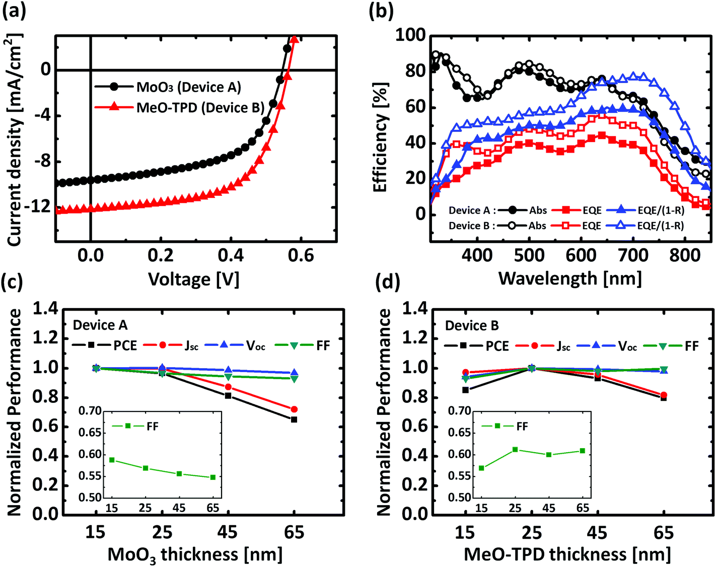 | ||
| Fig. 3 Performance and spectral response of inverted ZnPc:C70 devices with different optical spacers. (a) J–V characteristics of inverted devices with the MoO3 layer and with the p-MeO-TPD layer. (b) Absorption, EQE, and EQE/(1 − R) of inverted devices with the MoO3 layer (filled symbols) and the MeO-TPD layer (open symbols). Normalized values of solar cell parameters as a function of the thickness of (c) MoO3 layer, and (d) MeO-TPD layer. Insets represent FF values of both devices. | ||
Fig. 3(c) and (d) show the electrical performance of the devices as a function of the optical spacer thickness. The value Voc for both devices was independent of the thickness. In both cases, Jsc was maximized upon inserting 25 nm-thick optical spacer layers, in which the absorption was maximized in the active layer and decreased in the thicker layer. Reduction of Jsc was dramatic in device A due to severe degradation of IQE with the increased thickness of the HTL layer. EQE/(1 − R) data for each device according to the optical spacer thickness are presented in Fig. S3.† Two devices showed different FF tendencies according to the thickness of the optical spacer, as can be seen in the insets of Fig. 3(c) and (d). The value of FF of device A was found to almost linearly decrease when the MoO3 thickness was increased further; this decrease seemed to be caused by the low conductivity of the MoO3 layer.43,44 In contrast, the value of FF of device B did not decrease because p-MeO-TPD can be sufficiently thick without electrical loss due to the enhanced conductivity conferred by doping.
Fig. 4(a) shows the normalized EQE/(1 − R) data according to the thickness of the optical spacer. EQE/(1 − R) data were normalized for a device with 15 nm optical spacers of each kind. For comparison, we plotted EQE/(1 − R) in the wavelength range of only 600–775 nm because the absorption of the optical spacer can be ignored in this range. The reason for choosing that range is presented in Fig. S3.† Therefore, we could treat EQE/(1 − R) as the actual IQE of the device. The IQE of device A was found to decrease with an increase of the MoO3 thickness. Noticeably, however, the IQE of device B was nearly independent of the MeO-TPD thickness. IQE was related to the efficiencies of the exciton diffusion, charge transfer, and charge collection.35 Among these, only the charge transport efficiency was affected because we simply changed the thickness of the optical spacer. The low conductivity of MoO3 hinders efficient charge transport in MoO3 devices, in contrast to the case of the unaffected IQE of the MeO-TPD device. Therefore, using an optical spacer with high conductivity can optically optimize the device properties without IQE loss.
 | ||
| Fig. 4 Normalized EQE/(1 − R) and hole mobility data of MoO3 and MeO-TPD devices. (a) Normalized EQE/(1 − R) data of inverted devices with MoO3 and MeO-TPD layers according to their thicknesses. (b) Current density of hole-only devices with MoO3 and MeO-TPD layers. | ||
In addition, conductivity and hole mobility data are summarized in Table 2. The conductivity of p-MeO-TPD was greatly enhanced to 4.69 ± 2.22 × 10⁻⁴ S cm−1, suggesting that p-type doping was effectively done.27Fig. 4(b) shows the current density of hole-only devices with MoO3 and MeO-TPD. The hole mobility of each device was estimated using the space charge limited current (SCLC) method.45 The hole mobilities of MoO3 and MeO-TPD devices were 1.03 × 10⁻³ cm2 V−1 S−1 and 2.26 × 10⁻³ cm2 V−1 S−1, respectively; the MeO-TPD device showed an approximately two-fold higher level mobility than that of the MoO3 device. This high hole mobility can help charges balance inside a device, securing enhanced FF and IQE for a device with p-MeO-TPD compared to the MoO3 device of the same thickness.41,46 Consequently, the p-MeO-TPD device can be optically optimized without any electrical loss in contrast to the MoO3 device.
| Optical spacer | Conductivity [S cm−1] | Hole mobility [cm2 V−1 S−1] |
|---|---|---|
| MoO3 | 1.95 ± 0.84 × 10⁻⁶ | 1.03 ± 0.29 × 10⁻³ |
| p-MeO-TPD | 4.69 ± 2.22 × 10⁻⁴ | 2.26 ± 0.30 × 10⁻³ |
Improved stability of devices
Next, we fabricated both normal and inverted devices and stored them under ambient conditions. The normal device structure was ITO (75 nm)/MoO3 (10 nm)/ZnPc:C70 (30 nm)/C70 (20 nm)/BCP (8 nm)/Al (150 nm). Fig. 5(a) shows the PCE change of the OSCs for 40 days (∼1000 hours). The stabilities of device A and device B were greatly enhanced compared to that of the normal type devices, despite the use of the same active material system. Particularly, device B maintained its PCE value of 70% of the initial value after 40 days. On the other hand, the PCE of the normal device was almost impossible to measure after only a few days.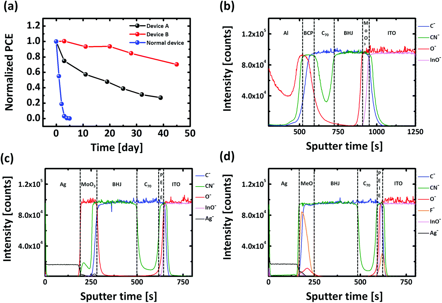 | ||
| Fig. 5 Stability results for normal and inverted ZnPc:C70 devices. (a) Normalized PCEs of the normal device and two inverted devices with MoO3 (device A) and MeO-TPD (device B) layers, both of which were stored under ambient conditions. Time-of-flight secondary ion mass spectrometry (TOF-SIMS) depth profiles of (b) normal devices and that of the inverted device (c) with the MoO3 layer (device A), and (d) with the MeO-TPD layer (device B). | ||
To investigate the improved stability of the inverted structure in more detail, we took time-of-flight secondary ion mass spectrometry (TOF-SIMS) depth profiles of both normal and inverted type devices that were stored under ambient conditions. Fig. 5(b) shows the TOF-SIMS results for the normal device. CN− is a mass spectral marker for BCP and ZnPc; F−, InO−, and Ag− are markers for F6-TCNNQ, the ITO electrode, and the top electrode of the inverted device, respectively. Note that C− represents all organic layers. O− is a key element related to the degradation of the devices. Oxygen seems to penetrate the Al electrode, especially into the BCP layer in the structure, explaining the serious degradation of the OSCs.35,47Fig. 5(c) and (d) show the TOF-SIMS results of the inverted devices A and B, respectively. There was no clear evidence of oxygen penetration in the active layers; only the intrinsic oxygen was observed at the MeO-TPD and MoO3 layers. Furthermore, device B was shown to have stability higher than that of device A, as can be seen in Fig. 5(a), implying that a MeO-TPD layer provides more robust protection against oxygen compared to a MoO3 layer. Further investigation is in progress to understand factors that cause instability of SMOSCs.
Conclusions
In summary, we demonstrated that an inverted structure of SMOSCs using a p-MeO-TPD layer showed both high PCE and improved stability. We were able to optimize the device performance by effectively adjusting the optical field distribution inside the device. Doped MeO-TPD is an attractive material as an optical spacer; because of its high conductivity and large optical band gap, it can be used to manipulate the optical effect without electrical loss in thin film optoelectronic devices. The PCEs of inverted ZnPc:C70 devices were enhanced from 3.00% to 4.15% upon replacement of a conventional MoO3 layer with a p-doped MeO-TPD layer because of the enhanced FF and IQE, which were mainly caused by the electrical benefit of p-MeO-TPD. Furthermore, the stability of the inverted devices was also significantly improved. This result will be useful in facilitating the commercialization of small molecular organic solar cells with improved stability.Experimental
Material preparation
Zinc phthalocyanine (ZnPc, EM index Co., Korea) was sublimated three times for purification. Fullerene (C60 and C70, 99.9%, EM index Co., Korea) and N,N,N′,N′-tetrakis(4-methoxyphenyl)benzidine (MeO-TPD, >99%, Lumtec, Taiwan) were sublimed twice. 2,2-(Perfluoronaphthalene-2,6-diylidene)dimalononitrile (F6-TCNNQ, Novaled AG., Germany) and acridine orange base (AOB, Aldrich) were used as a p-type and n-type dopant, respectively. Polyethylenimine, 80% ethoxylated, 35–40 wt% solution in water (Aldrich) was diluted with 2-methoxyethanol (Aldrich) to prepare a 0.4 wt% polyethylenimine ethoxylated (PEIE) solution. ITO (30 Ω per sq, JM International Co., Korea) substrates were cleaned in DI water with a detergent for 25 min and sequentially sonicated in acetone and isopropanol for 25 min.OSC device fabrication
Author contributions
S. L and J. L. conceived and designed the experiments and prepared the manuscript. S. L. and J. S. fabricated the organic solar cell devices and S. L. performed the optical simulations and measurements such as the determination of the J–V characteristics, EQE, absorption, and TOF-SIMS depth profiles. All authors discussed the results and commented on the manuscript.Acknowledgements
We also gratefully acknowledge support from the Center for Inorganic Photovoltaic Materials (2012-0001172), through a grant funded by the Ministry of Education, Science and Technology (MEST), the New & Renewable Energy Core Technology Program of the Korea Institute of Energy Technology Evaluation and Planning (KETEP), granted financial resource from the Ministry of Trade, Industry & Energy, Republic of Korea (no. 20133030000130) and grant no. EEWS-2014-N01140052 from the EEWS Research Project of the office of the KAIST EEWS Initiative, KAIST Institute for the NanoCentury.References
- M. A. Green, K. Emery, Y. Hishikawa, W. Warta and E. D. Dunlop, Solar cell efficiency tables (version 42), Prog. Photovoltaics, 2013, 21, 827–837 Search PubMed.
- P. Peumans, S. Uchida and S. R. Forrest, Efficient bulk heterojunction photovoltaic cells using small-molecular-weight organic thin films, Nature, 2003, 425, 158–162 CrossRef CAS PubMed.
- Y. Liang, Z. Xu, J. Xia, S.-T. Tsai, Y. Wu, G. Li, C. Ray and L. Yu, For the Bright Future-Bulk Heterojunction Polymer Solar Cells with Power Conversion Efficiency of 7.4%, Adv. Mater., 2010, 22, E135–E138 CrossRef CAS PubMed.
- R. Fitzner, E. Reinold, A. Mishra, E. Mena-Osteritz, H. Ziehlke, C. Korner, K. Leo, M. Riede, M. Weil, O. Tsaryova, A. Weiss, C. Uhrich, M. Pfeiffer and P. Bauerle, Dicyanovinyl-Substituted Oligothiophenes: Structure-Property Relationships and Application in Vacuum-Processed Small-Molecule Organic Solar Cells, Adv. Funct. Mater., 2011, 21, 897–910 CrossRef CAS.
- Heliatek press release (http://www.heliatek.com., January 16, 2013).
- J. B. You, L. T. Dou, K. Yoshimura, T. Kato, K. Ohya, T. Moriarty, K. Emery, C. C. Chen, J. Gao, G. Li and Y. Yang, A polymer tandem solar cell with 10.6% power conversion efficiency, Nat. Commun., 2013, 4, 1446 CrossRef PubMed.
- J. Y. Kim, S. H. Kim, H. H. Lee, K. Lee, W. L. Ma, X. Gong and A. J. Heeger, New architecture for high-efficiency polymer photovoltaic cells using solution-based titanium oxide as an optical spacer, Adv. Mater., 2006, 18, 572–576 CrossRef CAS.
- J. Gilot, I. Barbu, M. M. Wienk and R. A. J. Janssen, The use of ZnO as optical spacer in polymer solar cells: Theoretical and experimental study, Appl. Phys. Lett., 2007, 91, 113520 CrossRef PubMed.
- S. H. Park, A. Roy, S. Beaupre, S. Cho, N. Coates, J. S. Moon, D. Moses, M. Leclerc, K. Lee and A. J. Heeger, Bulk heterojunction solar cells with internal quantum efficiency approaching 100%, Nat. Photonics, 2009, 3, 297–U295 CrossRef CAS.
- A. K. K. Kyaw, D. H. Wang, D. Wynands, J. Zhang, T.-Q. Nguyen, G. C. Bazan and A. J. Heeger, Improved Light Harvesting and Improved Efficiency by Insertion of an Optical Spacer (ZnO) in Solution-Processed Small-Molecule Solar Cells, Nano Lett., 2013, 3796–3801 CrossRef CAS PubMed.
- C. H. Hsieh, Y. J. Cheng, P. J. Li, C. H. Chen, M. Dubosc, R. M. Liang and C. S. Hsu, Highly Efficient and Stable Inverted Polymer Solar Cells Integrated with a Cross-Linked Fullerene Material as an Interlayer, J. Am. Chem. Soc., 2010, 132, 4887–4893 CrossRef CAS PubMed.
- F. C. Krebs, Air stable polymer photovoltaics based on a process free from vacuum steps and fullerenes, Sol. Energy Mater. Sol. Cells, 2008, 92, 715–726 CrossRef CAS PubMed.
- Y. Sahin, S. Alem, R. de Bettignies and J. M. Nunzi, Development of air stable polymer solar cells using an inverted gold on top anode structure, Thin Solid Films, 2005, 476, 340–343 CrossRef CAS PubMed.
- K. Norrman, M. V. Madsen, S. A. Gevorgyan and F. C. Krebs, Degradation Patterns in Water and Oxygen of an Inverted Polymer Solar Cell, J. Am. Chem. Soc., 2010, 132, 16883–16892 CrossRef CAS PubMed.
- Q. L. Song, M. L. Wang, E. G. Obbard, X. Y. Sun, X. M. Ding, X. Y. Hou and C. M. Li, Degradation of small-molecule organic solar cells, Appl. Phys. Lett., 2006, 89, 251118 CrossRef PubMed.
- X. R. Tong, R. F. Bailey-Salzman, G. D. Wei and S. R. Forrest, Inverted small molecule organic photovoltaic cells on reflective substrates, Appl. Phys. Lett., 2008, 93, 173304 CrossRef PubMed.
- M. F. Xu, X. B. Shi, Z. M. Jin, F. S. Zu, Y. Liu, L. Zhang, Z. K. Wang and L. S. Liao, Aqueous Solution-Processed GeO2: An Anode Interfacial Layer for High Performance and Air-Stable Organic Solar Cells, Acs Appl. Mater. Interfaces, 2013, 5, 10866–10873 CAS.
- M.-F. Xu, L.-S. Cui, X.-Z. Zhu, C.-H. Gao, X.-B. Shi, Z.-M. Jin, Z.-K. Wang and L.-S. Liao, Aqueous solution-processed MoO3 as an effective interfacial layer in polymer/fullerene based organic solar cells, Org. Electron., 2013, 14, 657–664 CrossRef CAS PubMed.
- B. Lussem, M. Riede and K. Leo, Doping of organic semiconductors, Phys. Status Solidi A, 2013, 210, 9–43 CrossRef.
- K. Walzer, B. Maennig, M. Pfeiffer and K. Leo, Highly efficient organic devices based on electrically doped transport layers, Chem. Rev., 2007, 107, 1233–1271 CrossRef CAS PubMed.
- R. Timmreck, S. Olthof, K. Leo and M. K. Riede, Highly doped layers as efficient electron-hole recombination contacts for tandem organic solar cells, J. Appl. Phys., 2010, 108, 033108 CrossRef PubMed.
- M. Riede, C. Uhrich, J. Widmer, R. Timmreck, D. Wynands, G. Schwartz, W. M. Gnehr, D. Hildebrandt, A. Weiss, J. Hwang, S. Sundarraj, P. Erk, M. Pfeiffer and K. Leo, Efficient Organic Tandem Solar Cells based on Small Molecules, Adv. Funct. Mater., 2011, 21, 3019–3028 CrossRef CAS.
- Y. H. Zhou, C. Fuentes-Hernandez, J. Shim, J. Meyer, A. J. Giordano, H. Li, P. Winget, T. Papadopoulos, H. Cheun, J. Kim, M. Fenoll, A. Dindar, W. Haske, E. Najafabadi, T. M. Khan, H. Sojoudi, S. Barlow, S. Graham, J. L. Bredas, S. R. Marder, A. Kahn and B. Kippelen, A Universal Method to Produce Low-Work Function Electrodes for Organic Electronics, Science, 2012, 336, 327–332 CrossRef CAS PubMed.
- Y. H. Kim, T. H. Han, H. Cho, S. Y. Min, C. L. Lee and T. W. Lee, Polyethylene Imine as an Ideal Interlayer for Highly Efficient Inverted Polymer Light-Emitting Diodes, Adv. Funct. Mater., 2014, 24, 3808–3814 CrossRef CAS.
- G. F. He, M. Pfeiffer, K. Leo, M. Hofmann, J. Birnstock, R. Pudzich and J. Salbeck, High-efficiency and low-voltage p-i-n electrophosphorescent organic light-emitting diodes with double-emission layers, Appl. Phys. Lett., 2004, 85, 3911–3913 CrossRef CAS PubMed.
- X. Zhou, M. Pfeiffer, J. Blochwitz, A. Werner, A. Nollau, T. Fritz and K. Leo, Very-low-operating-voltage organic light-emitting diodes using a p-doped amorphous hole injection layer, Appl. Phys. Lett., 2001, 78, 410–412 CrossRef CAS PubMed.
- M. L. Tietze, L. Burtone, M. Riede, B. Lussem and K. Leo, Fermi level shift and doping efficiency in p-doped small molecule organic semiconductors: A photoelectron spectroscopy and theoretical study, Phys. Rev. B: Condens. Matter, 2012, 86, 035320 CrossRef.
- J. Meiss, A. Merten, M. Hein, C. Schuenemann, S. Schafer, M. Tietze, C. Uhrich, M. Pfeiffer, K. Leo and M. Riede, Fluorinated Zinc Phthalocyanine as Donor for Efficient Vacuum-Deposited Organic Solar Cells, Adv. Funct. Mater., 2012, 22, 405–414 CrossRef CAS.
- C. Schunemann, D. Wynands, L. Wilde, M. P. Hein, S. Pfutzner, C. Elschner, K. J. Eichhorn, K. Leo and M. Riede, Phase separation analysis of bulk heterojunctions in small-molecule organic solar cells using zinc-phthalocyanine and C-60, Phys. Rev. B: Condens. Matter, 2012, 85, 245314 CrossRef.
- C. Falkenberg, Ph.D. Thesis, Technische Universität Dresden, 2011.
- A. K. K. Kyaw, D. H. Wang, V. Gupta, J. Zhang, S. Chand, G. C. Bazan and A. J. Heeger, Efficient Solution-Processed Small-Molecule Solar Cells with Inverted Structure, Adv. Mater., 2013, 25, 2397–2402 CrossRef CAS PubMed.
- J. Blochwitz, T. Fritz, M. Pfeiffer, K. Leo, D. M. Alloway, P. A. Lee and N. R. Armstrong, Interface electronic structure of organic semiconductors with controlled doping levels, Org. Electron., 2001, 2, 97–104 CrossRef CAS.
- R. Meerheim, S. Olthof, M. Hermenau, S. Scholz, A. Petrich, N. Tessler, O. Solomeshch, B. Lussem, M. Riede and K. Leo, Investigation of C(60)F(36) as low-volatility p-dopant in organic optoelectronic devices, J. Appl. Phys., 2011, 109, 103102 CrossRef PubMed.
- L. A. A. Pettersson, L. S. Roman and O. Inganas, Modeling photocurrent action spectra of photovoltaic devices based on organic thin films, J. Appl. Phys., 1999, 86, 487–496 CrossRef CAS PubMed.
- P. Peumans, A. Yakimov and S. R. Forrest, Small molecular weight organic thin-film photodetectors and solar cells, J. Appl. Phys., 2003, 93, 3693–3723 CrossRef CAS PubMed.
- B. Verreet, R. Muller, B. P. Rand, K. Vasseur and P. Heremans, Structural templating of chloro-aluminum phthalocyanine layers for planar and bulk heterojunction organic solar cells, Org. Electron., 2011, 12, 2131–2139 CrossRef CAS PubMed.
- M. L. Zhang, H. Wang, H. K. Tian, Y. H. Geng and C. W. Tang, Bulk Heterojunction Photovoltaic Cells with Low Donor Concentration, Adv. Mater., 2011, 23, 4960–4964 CrossRef CAS PubMed.
- X. Xiao, J. D. Zimmerman, B. E. Lassiter, K. J. Bergemann and S. R. Forrest, A hybrid planar-mixed tetraphenyldibenzoperiflanthene/C-70 photovoltaic cell, Appl. Phys. Lett., 2013, 102, 073302 CrossRef PubMed.
- S. Pfuetzner, J. Meiss, A. Petrich, M. Riede and K. Leo, Improved bulk heterojunction organic solar cells employing C70 fullerenes, Appl. Phys. Lett., 2009, 94, 223307 CrossRef PubMed.
- W. Tress, K. Leo and M. Riede, Effect of concentration gradients in ZnPc:C-60 bulk heterojunction organic solar cells, Sol. Energy Mater. Sol. Cells, 2011, 95, 2981–2986 CAS.
- W. Tress, A. Merten, M. Furno, M. Hein, K. Leo and M. Riede, Correlation of Absorption Profile and Fill Factor in Organic Solar Cells: The Role of Mobility Imbalance, Adv. Energy Mater., 2013, 3, 631–638 CrossRef CAS.
- Y. Zhou, T. Taima, T. Miyadera, T. Yamanari, M. Kitamura, K. Nakatsu and Y. Yoshida, Phase separation of co-evaporated ZnPc:C-60 blend film for highly efficient organic photovoltaics, Appl. Phys. Lett., 2012, 100, 233302 CrossRef PubMed.
- N. Miyata, T. Suzuki and R. Ohyama, Physical properties of evaporated molybdenum oxide films, Thin Solid Films, 1996, 282, 218–222 CrossRef.
- G. S. Nadkarni and J. G. Simmons, Electrical properties of evaporated molybdenum oxide films, J. Appl. Phys., 1970, 41, 545–551 CrossRef CAS PubMed.
- A. Wagenpfahl, D. Rauh, M. Binder, C. Deibel and V. Dyakonov, S-shaped current-voltage characteristics of organic solar devices, Phys. Rev. B: Condens. Matter, 2010, 82, 115306 CrossRef.
- X. G. Guo, N. J. Zhou, S. J. Lou, J. Smith, D. B. Tice, J. W. Hennek, R. P. Ortiz, J. T. L. Navarrete, S. Y. Li, J. Strzalka, L. X. Chen, R. P. H. Chang, A. Facchetti and T. J. Marks, Polymer solar cells with enhanced fill factors, Nat. Photonics, 2013, 7, 825–833 CrossRef CAS.
- Q. L. Song, F. Y. Li, H. Yang, H. R. Wu, X. Z. Wang, W. Zhou, J. M. Zhao, X. M. Ding, C. H. Huang and X. Y. Hou, Small-molecule organic solar cells with improved stability, Chem. Phys. Lett., 2005, 416, 42–46 CrossRef CAS PubMed.
Footnote |
| † Electronic supplementary information (ESI) available. See DOI: 10.1039/c4nr05425c |
| This journal is © The Royal Society of Chemistry 2015 |