The CVD graphene transfer procedure introduces metallic impurities which alter the graphene electrochemical properties†
Adriano
Ambrosi
and
Martin
Pumera
*
Division of Chemistry & Biological Chemistry, School of Physical and Mathematical Sciences, Nanyang Technological University, Singapore 637371, Singapore. E-mail: pumera@ntu.edu.sg; Pumera@outlook.com
First published on 11th November 2013
Abstract
High quality graphene films can be fabricated by chemical vapor deposition (CVD) using Ni and Cu as catalytic substrates. Such a synthesis procedure always requires a subsequent transfer process to be performed in order to eliminate the metallic substrate and transfer the graphene onto the desired surface. We show here that such a transfer process causes significant contamination of the graphene film with residual Fe and Ni metal impurities. Fe contamination derives from the use of Fe-based etching solutions to dissolve Ni (or Cu) substrates, while residual Ni (or Cu) is due to an incomplete metal substrate etching. The presence of these metallic impurities within the transferred graphene film affects tremendously its electrochemical behavior when adopted as an electrode material.
Introduction
Chemical vapor deposition (CVD) represents one of the most promising fabrication procedures to generate large area and high quality graphene films1 for applications such as transparent conductive electrodes,2 electronic transistors,3 electrochemical devices,4,5 thermal conductors,6 and corrosion- or oxidation-inhibiting coatings.7–9 The most remarkable results in terms of quality and large volume production of CVD graphene were recently achieved using nickel or copper as substrates to facilitate the production of single or few layer graphene films.10–15 With abundant availability and the low cost of nickel and copper, these are also the most widely used metal substrates. Despite the enormous advances achieved for the CVD method, the reproducibility of the fabrication method for large area and defect-less graphene still remains very challenging.11 In addition, it is important to mention that graphene fabricated by the CVD method requires a subsequent transfer process which includes the removal of metallic substrates and transfer of the graphene film onto desired surfaces depending on the applications.16 Even if a CVD graphene film possesses low level of defects and very high carrier mobility and conductivity, the degradation of such properties is almost unavoidable during the transfer process since chemical alterations and mechanical damage are likely generated.17 Current research efforts are, in fact, directed to the improvement of the transfer process.16 Regardless of whether the graphene transfer process is polymer supported, the procedure always requires the removal of the metal catalyst substrate (Ni and Cu). This is usually achieved using oxidant-etchant solutions such as FeCl3 and Fe(NO3)3 or occasionally with (NH4)2S2O8.16 The metal etching represents a key step in the transfer process since an incomplete etching and a poor removal of the etching solution could cause significant contamination of the graphene film with metallic species (Fe, Cu, and Ni).The presence of metallic impurities within carbon materials such as carbon nanotubes and graphene has been largely documented.18 Following the previous scenarios with carbon nanotubes19–27 we showed that metal impurities are also present within graphene materials fabricated by the top-down methods using graphite as the starting material and that such residual impurities resulted in a significant alteration of the electrochemical behaviour of the materials.28,29 It has also been theoretically predicted that the presence of metallic impurities alters significantly the electronic properties of graphene.30,31
Here we focus our attention to the graphene material fabricated by the bottom-up CVD method and show that metallic impurities can easily be introduced during the transfer step. As proof-of-concept we employed commercially available graphene samples grown on Ni foil. Adopting Fe based etching solutions for the removal of the Ni substrate resulted in a minimal but significant contamination of the transferred graphene film with residual Fe impurities. In addition, Ni impurities remain linked to the graphene film due to an incomplete etching process. We demonstrate here that such metallic impurities can cause a tremendous alteration of the electrochemical properties of the graphene film when applied as an electrode material.
Experimental
Materials
CVD multilayer graphene grown on Ni foil was purchased from Graphene Laboratories Inc., NY, USA and cumene hydroperoxide (CHP) (80%) was purchased from Alfa Aesar. Sodium hydroxide, potassium phosphate disodium salt, and iron(III) chloride were purchased from Sigma-Aldrich, Singapore. Edge-plane pyrolytic graphite (EPPG) and basal-plane pyrolytic graphite (BPPG) electrodes with a diameter of 3 mm were obtained from Autolab, Japan.Apparatus
A JEOL-7600F semi-in-lens FE-SEM, operating in TED mode at 30 kV, was used to acquire the STEM images and perform Energy Dispersive X-ray (EDX) analysis. Small pieces of graphene samples floating on the solution after the washing step were carefully loaded onto a TEM grid.All voltammetric experiments were performed on an Autolab PGSTAT101 electrochemical analyzer (Methrom Autolab B. V., The Netherlands) connected to a personal computer and controlled by NOVA software Version 1.8 (Methrom Autolab B. V.). Elemental analysis (Agilent model 7700× ICP-MS) was performed by dissolving few transferred graphene samples in ultrapure nitric acid (10%) before microwave digestion (Mars CEM system).
Procedures
CVD-graphene samples with an approximate size of 1 cm2 were initially polished with care on one of the sides with a fine abrasive paper to remove the graphene film and expose that side of the Ni foil, while leaving the graphene film on the other side untouched. The CVD graphene samples were then left floating on a FeCl3 (0.1 g mL−1) solution for at least 2 h or until complete dissolution of the Ni metals was achieved. The floating graphene films were then transferred with a spoon to a distilled water solution to remove the excess FeCl3. Transferring of the graphene films to a clean DI water solution was repeated at least 5 times to maximize the removal of excess FeCl3. A clean glass slide was then used to pull-out each graphene film from the water solution for the final stage of the transfer process. The glass substrates with the transferred graphene film were then gently heated at 40 °C in a vacuum oven for 5 h to eliminate any residual water and facilitate the adhesion.Electrochemical experiments were performed at room temperature by using a three-electrode configuration. A platinum electrode (Autolab) served as an auxiliary electrode, while an Ag/AgCl electrode (CH Instruments, USA) served as a reference electrode. A custom-made voltammetric cell (see Fig. S1†) was used to contain the CVD graphene transferred onto a glass slide as a working electrode. A normal 5 mL glass cell was adopted to test EPPG and BPPG working electrodes. All electrochemical potentials in this paper are stated versus the Ag/AgCl reference electrode. The EPPG and GC electrode surfaces were renewed by polishing with 0.05 mm alumina particles on a cloth and sonicated in ethanol and deionized water for 10 min each to remove any adhered microparticles of alumina. The BPPG electrode surface was renewed by pressing the surface onto an adhesive tape and removing the top few layers of graphite. This was repeated several times before rinsing the electrode surface in acetone to remove any residual adhesive glue. Cyclic voltammetry experiments were performed at a scan rate of 100 mV s−1 by using 50 mM phosphate buffer (pH 7.2) for cumene hydroperoxide (CHP); 0.1 M NaOH solution was employed as the supporting electrolyte when testing for the presence of residual Ni following the procedure published elsewhere.27,32,33
Results and discussions
Fig. 1 illustrates the typical steps involved during the transfer of a CVD-grown graphene to an arbitrary surface after the removal of the metal substrate. In this work, samples of multilayer graphene grown by CVD on Ni foil were adopted for analysis. This type of sample was selected because it simplifies the transfer procedure which can be carried out without any polymeric support (e.g. PMMA, PDMS). Polymeric supports are normally employed to facilitate the transfer of mono-few layer thick graphene films grown in particular on Cu foils12 or thin Ni films.15 While being indispensible to transfer such delicate graphene samples, the use of polymeric scaffolds introduces extra steps to the transfer process increasing the risk of structural damage and contamination.16 Since electronic and electrocatalytic properties of graphene are known to be altered by the presence of metallic impurities28–31 we primarily focused in this work on the consequences of the etching process that represents also the main source of metallic contamination.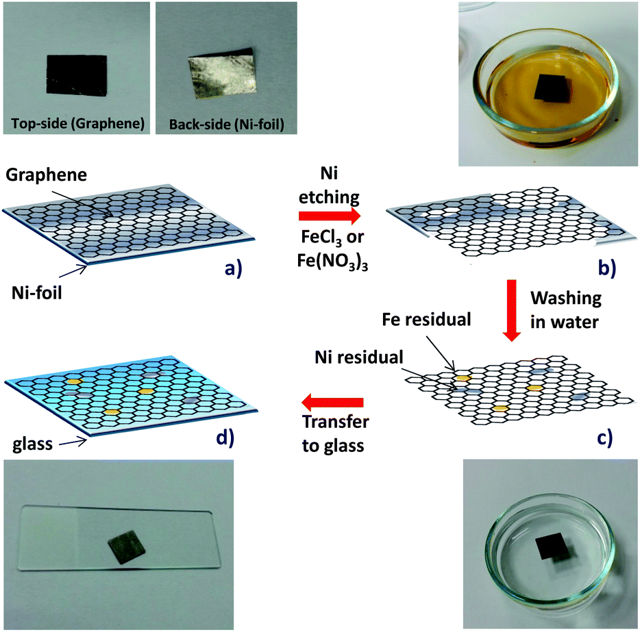 | ||
| Fig. 1 Schematic of the adopted transfer process. (a) CVD-multilayer graphene sample grown on Ni foil has been polished at one side to remove the graphene film and facilitate the exposure of the Ni foil. (b) Ni metal is etched away using FeCl3 (or Fe(NO3)3) solution. (c) After complete dissolution of Ni, the graphene film is then transferred into a clean distilled water solution. This is done several times to remove the excess Fe-based etching solution. (d) The graphene film is transferred to a clean glass slide. Despite the careful etching and washing steps, the contamination from remaining Ni and Fe metals was unavoidable (indicated as grey and yellow dots, respectively). | ||
Initially, the underside of a 1 cm2 sample was polished to remove the graphene film and to facilitate the exposure of Ni metal. On the upper side, the graphene film remained untouched. Prior to the transfer of the graphene film onto an arbitrary surface, it is necessary to remove the metal catalyst substrate.
Graphene samples grown on Ni and Cu metal substrates are typically treated with Fe(III) based etching solution to dissolve the metals by oxidizing metallic Ni(0) and Cu(0) to soluble Ni(II) and Cu(II) cations, respectively. In order to avoid any contamination at this point, it is crucial to make sure that the metal substrate is completely dissolved with no residual metal remaining unetched and that the excess etching solution (Fe(III)) is washed away. Consequently, a prolonged etching time (>2 h) should address the first concern while several washing steps with distilled water should ensure the elimination of excess etching solution from the graphene film. This etching and washing procedure was carried out as described in several studies.10,11,16 After the washing steps, the graphene film was transferred to an arbitrary surface, i.e. glass for this specific work. We evaluated this transfer procedure by varying the etching time and washing patterns only to reveal that the transferred graphene film was always contaminated by a variable amount of both Fe and Ni impurities in all cases (indicated in Fig. 1 as yellow and grey dots, respectively).
In order to demonstrate the presence of Fe and Ni impurities, we carried out various analyses. Inductively-coupled plasma with mass-spectroscopy (ICP-MS) is one of the most reliable elemental analysis techniques with a detection limit in the sub-ppb region. For a direct analysis on the transferred graphene films, three graphene films were transferred onto glass slides as illustrated in Fig. 1 after several washings with distilled water to remove excess etching solution. After ensuring complete drying and adhesion of the graphene films onto the glass slides, the graphene films were gently removed using 10% ultrapure nitric acid with the help of a glass rod.
The three graphene films were then collected into a tube filled with 1 mL of HNO3. The ICP-MS analysis of such a sample resulted with about 13 ppm of Fe, 0.2 ppm of Ni and ppb levels of Zn, Cu and Co. The Fe and Ni were clearly the most abundant elements detected. Apart from that, the graphene films were also analyzed after the washing steps by means of STEM/EDX. Fig. 2 shows an STEM image of the graphene films with disseminated darker spots on the material surface (for other STEM images see Fig. S2† of ESI). EDX analysis of the area investigated (Fig. 2B) confirmed the presence of Fe. Similar results obtained from several other samples strongly supported the findings of the ICP-MS analysis. Ni impurities were not detected by the EDX technique due to both the lower concentration of Ni as compared to Fe and the insufficient sensitivity of the EDX technique.
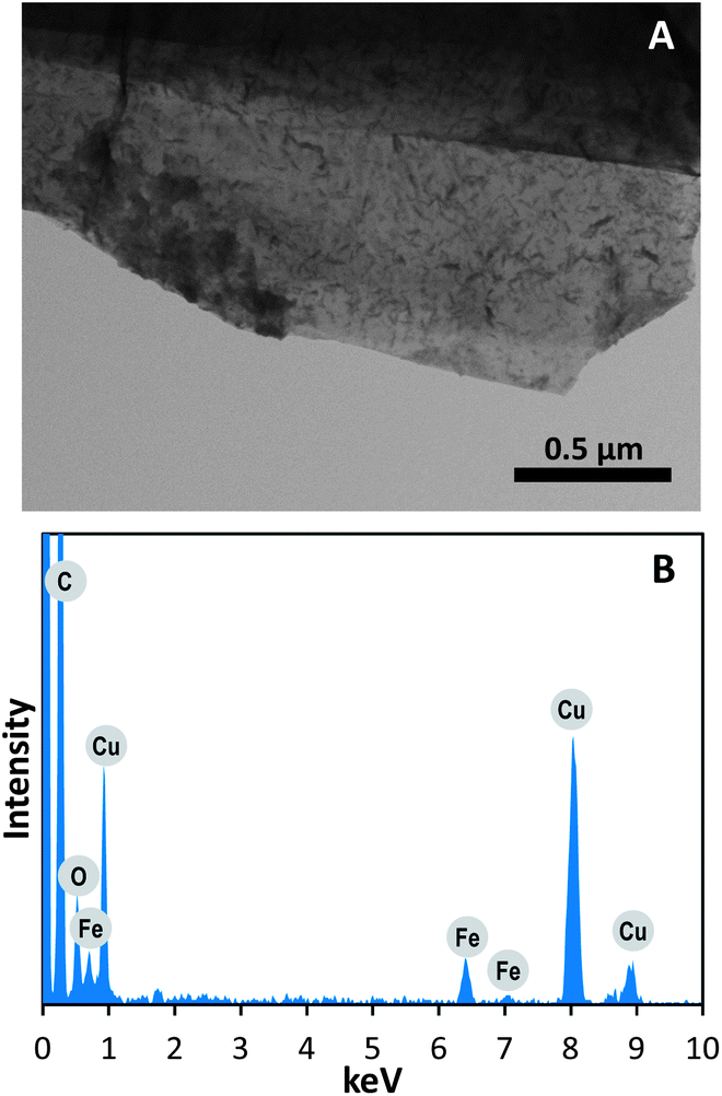 | ||
| Fig. 2 (A) STEM images of graphene films loaded onto C/Cu TEM grids after the washing procedures showing surfaces with darker spots disseminated. (B) Energy dispersive (EDX) analysis confirmed the presence of Fe metal. Note that Cu signals were derived from the C/Cu TEM grid used for the analysis. | ||
Furthermore, a Ni-specific analysis was conducted based on a known electrochemical investigation to probe the presence of Ni impurities in the graphene samples.27,32,33
It is well-known that in alkaline solutions, Ni metal spontaneously generates a thin layer of Ni(OH)2 which can be electrochemically oxidized to NiOOH according to the reaction:34,35
| Ni(OH)2 → NiOOH + H+ + e− | (1) |
Successive potential cycling causes the thickening of the Ni(OH)2 layer which is directly observable and represented by the increment of the oxidative and reductive peaks in cyclic voltammetry.36 One hundred voltammetric scans were performed in 0.1 M NaOH solution using the voltammetric cell described in Fig. S1† of the ESI and employing CVD graphene transferred onto glass (CVD-G-tr), as the working electrode. This was done such that in the presence of Ni metal, obvious growing behaviors of the redox peaks are visible by comparing several successive cyclic voltammograms (see Fig. S3† of the ESI for a complete set of voltammograms). Fig. 3A illustrates the 100th cyclic voltammetric scan which has the largest oxidative and reductive signals generated by the Ni metal using CVD-G-tr (blue line) in comparison to a pure Ni foil (black line). The oxidation and reduction peaks at about 0.4 V and 0.1 V corresponding to the oxidation of Ni(OH)2 to NiOOH and the reverse reduction, were clearly visible when Ni foil was used as a working electrode. This is a typical and well-known voltammetric behavior of Ni metals.27,37,38 The cyclic voltammogram recorded using the transferred CVD graphene presented significantly less intense signals but the typical oxidative and reductive signals (see enlarged graph as inset in Fig. 3A) were still clearly visible. This verified the presence of Ni metals within the graphene film. This sensitive electrochemical analysis thus confirmed the contamination from residual Ni metal derived from an incomplete etching. Upon confirmation of the presence of both Fe and Ni impurities within the transferred CVD graphene films using complementary techniques such as ICP-MS, STEM/EDX and cyclic voltammetry, we investigated possible effects of such impurities on the electrochemistry of the transferred graphene. It has been demonstrated in the past that peroxides are particularly sensitive to the presence of Fe impurities since they can catalyze the electrochemical reduction of the peroxides.20,28,29,39 As such, the electrochemical behaviors of several CVD-G-tr towards the reduction of cumene hydroperoxide (CHP) were tested in comparison to those of EPPG, GC and BPPG electrodes as reference electrode materials. It can be seen in Fig. 3B that the reduction of CHP using the CVD-G-tr electrode occurred at a potential of about −0.45 V which was significantly higher than those recorded using EPPG and GC electrodes (−0.75 V). The BPPG electrode presented a poorer electrochemical behavior with no clear reduction signal. It is evident that the CVD graphene film which should behave similar to EPPG or GC electrodes, presented an electrocatalytic response which can be attributed to the presence of Fe impurities.28,29
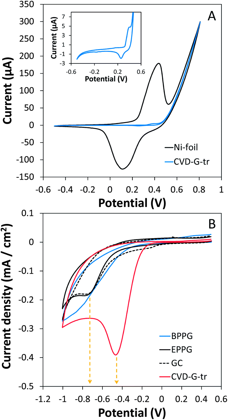 | ||
| Fig. 3 Electrochemical investigations. (A) Representative cyclic voltammograms (after 100 potential scans) performed in 0.1 M NaOH solution using clean Ni foil (black line) and transferred CVD graphene (blue line). (B) Representative cyclic voltammograms performed in phosphate buffered solution (pH 7.2) in the presence of 10 mM cumene hydroperoxide (CHP) and using EPPG (black line), BPPG (blue line), GC (black dotted line) and transferred CVD graphene (red line). | ||
Several studies have previously pointed out that the transfer procedure leads to metal contamination,40–42 but to date no work demonstrated practically what consequences these impurities may cause. Our results show for the first time that the metallic impurities introduced during the transfer procedure of CVD grown graphene alter tremendously the electrochemical behavior of the graphene material.
Conclusions
In conclusion, we have demonstrated that the procedures generally adopted to transfer CVD-grown graphene onto arbitrary surfaces, could cause contamination of the graphene films with metal impurities (Fe and Ni). In particular, Fe metal impurities could be introduced by the usage of FeCl3 or Fe(NO3)3 as etching solutions to dissolve the metal substrate prior to the graphene transfer. Although repeated washing with distilled water could remove most of the excess etching solution, a significant amount of residual Fe still remained. In addition, it was evident that small portions of the Ni metal substrate remained undissolved in the etching solution and were thus transferred along with the graphene film onto the new surface. We demonstrated that such impurities can alter the electrochemical behavior of the transferred graphene film when applied as an electrode material. In fact, Fe impurities provided an electrocatalytic capability to the transferred graphene film towards the reduction of cumene hydroperoxide. In light of these findings, we recommend that careful characterization should be performed after the graphene transfer process since trace amounts of metallic impurities could cause significant alterations to the electrochemical as well as electronic, optical and mechanical properties of the graphene material. Transfer procedures employing Fe-free etchants or alternative procedures which make use of chemical linkers to strongly bind the graphene and require no etching of the metal catalyst should also be taken into consideration to avoid as much as possible metal contamination, in particular when graphene is intended for electrochemical applications.Acknowledgements
The authors thank Dr Bahareh Khezri and Prof. Richard D. Webster for assistance with ICP-MS analysis. M.P. thanks MINDEF-NTU (#JPP-11-02-06) and NAP (NTU) funds for financial support.References
- C. Mattevi, H. Kim and M. Chhowalla, J. Mater. Chem., 2011, 21, 3324 RSC.
- X. Li, Y. Zhu, W. Cai, M. Borysiak, B. Han, D. Chen, R. D. Piner, L. Colombo and R. S. Ruoff, Nano Lett., 2009, 9, 4359 CrossRef CAS PubMed.
- D. Farmer, H.-Y. Chiu, Y.-M. Lin, K. Jenkins, F. Xia and P. Avouris, Nano Lett., 2009, 9, 4474 CrossRef CAS PubMed.
- A. Ambrosi and M. Pumera, J. Phys. Chem. C, 2013, 117, 2053 CAS.
- A. T. Valota, I. A. Kinloch, K. S. Novoselov, C. Casiraghi, A. Eckmann, E. W. Hill and R. A. W. Dryfe, ACS Nano, 2011, 5, 8809 CrossRef CAS PubMed.
- A. A. Balandin, S. Ghosh, W. Z. Bao, I. Calizo, D. Teweldebrhan, F. Miao and C. N. Lau, Nano Lett., 2008, 8, 902 CrossRef CAS PubMed.
- S. Chen, L. Brown, M. Levendorf, W. Cai, S.-Y. Ju, J. Edgeworth, X. Li, C. W. Magnuson, A. Velamakanni, R. D. Piner, J. Kang, J. Park and R. S. Ruoff, ACS Nano, 2011, 5, 1321 CrossRef CAS PubMed.
- D. Prasai, J. C. Tuberquia, R. R. Harl, G. K. Jennings and K. I. Bolotin, ACS Nano, 2012, 6, 1102 CrossRef CAS PubMed.
- J. Rafiee, X. Mi, H. Gullapalli, A. V. Thomas, F. Yavari, Y. Shi, P. M. Ajayan and N. A. Koratkar, Nat. Mater., 2012, 11, 217 CrossRef CAS PubMed.
- K. S. Kim, Y. Zhao, H. Jang, S. Y. Lee, J. M. Kim, K. S. Kim, J.-H. Ahn, P. Kim, J.-Y. Choi and B. H. Hong, Nature, 2009, 457, 706 CrossRef CAS PubMed.
- S. Bae, H. Kim, Y. Lee, X. Xu, J.-S. Park, Y. Zheng, J. Balakrishnan, T. Lei, H. Ri Kim, Y. I. Song, Y.-J. Kim, K. S. Kim, B. Ozyilmaz, J.-H. Ahn, B. H. Hong and S. Iijima, Nat. Nanotechnol., 2010, 5, 574 CrossRef CAS PubMed.
- X. Li, W. Cai, J. An, S. Kim, J. Nah, D. Yang, R. Piner, A. Velamakanni, I. Jung, E. Tutuc, S. K. Banerjee, L. Colombo and R. S. Ruoff, Science, 2009, 324, 1312 CrossRef CAS PubMed.
- X. Li, C. W. Magnuson, A. Venugopal, R. M. Tromp, J. B. Hannon, E. M. Vogel, L. Colombo and R. S. Ruoff, J. Am. Chem. Soc., 2011, 133, 2816 CrossRef CAS PubMed.
- Z. Sun, Z. Yan, J. Yao, E. Beitler, Y. Zhu and J. M. Tour, Nature, 2010, 468, 549 CrossRef CAS PubMed.
- A. Reina, X. Jia, J. Ho, D. Nezich, H. Son, V. Bulovic, M. S. Dresselhaus and J. Kong, Nano Lett., 2009, 9, 30 CrossRef CAS PubMed.
- J. Kang, D. Shin, S. Bae and B. Hong, Nanoscale, 2012, 4, 5527 RSC.
- S. K. Hong, S. M. Song, O. Sul and B. J. Cho, J. Electrochem. Soc., 2012, 159, K107 CrossRef CAS PubMed.
- M. Pumera, A. Ambrosi and E. L. K. Chng, Chem. Sci., 2012, 3, 3347 RSC.
- C. E. Banks, A. Crossley, C. Salter, S. J. Wilkins and R. G. Compton, Angew. Chem., Int. Ed., 2006, 45, 2533 CrossRef CAS PubMed.
- B. Sljukic, C. E. Banks and R. G. Compton, Nano Lett., 2006, 6, 1556 CrossRef CAS PubMed.
- C. Batchelor-McAuley, G. G. Wildgoose, R. G. Compton, L. D. Shao and M. L. H. Green, Sens. Actuators, B, 2008, 132, 356 CrossRef CAS PubMed.
- M. Pumera, H. Iwai and Y. Miyahara, ChemPhysChem, 2009, 10, 1770 CrossRef CAS PubMed.
- A. Ambrosi and M. Pumera, Chem.–Eur. J., 2010, 16, 1786 CrossRef CAS PubMed.
- E. J. E. Stuart and M. Pumera, Chem.–Asian J., 2011, 6, 1019 CrossRef CAS PubMed.
- E. L. K. Chng and M. Pumera, Chem.–Asian J., 2011, 6, 2304 CrossRef CAS PubMed.
- E. J. E. Stuart and M. Pumera, Phys. Chem. Chem. Phys., 2011, 13, 10818 RSC.
- A. Ambrosi and M. Pumera, Chem.–Eur. J., 2012, 18, 3338 CrossRef CAS PubMed.
- A. Ambrosi, S. Y. Chee, B. Khezri, R. D. Webster, Z. Sofer and M. Pumera, Angew. Chem., Int. Ed., 2012, 51, 500 CrossRef CAS PubMed.
- A. Ambrosi, C. K. Chua, B. Khezri, Z. Sofer, R. D. Webster and M. Pumera, Proc. Natl. Acad. Sci. U. S. A., 2012, 109, 12899 CrossRef CAS PubMed.
- A. V. Krasheninnikov and R. M. Nieminen, Theor. Chem. Acc., 2011, 129, 625 CrossRef CAS PubMed.
- F. M. Hu, T. X. Ma, H. Q. Lin and J. E. Gubernatis, Phys. Rev. B: Condens. Matter Mater. Phys., 2011, 84, 075414 CrossRef.
- A. Ambrosi, A. Bonanni, Z. Sofer and M. Pumera, Nanoscale, 2013, 5, 2379 RSC.
- M. Giovanni, A. Ambrosi and M. Pumera, Chem.–Asian J., 2012, 7, 702 CrossRef CAS PubMed.
- D. Giovanelli, N. S. Lawrence, L. Jiang, T. G. J. Jones and R. G. Compton, Sens. Actuators, B, 2003, 88, 320 CrossRef CAS.
- K. E. Toghill, L. Xiao, N. R. Stradiotto and R. G. Compton, Electroanalysis, 2010, 22, 491 CrossRef CAS.
- S. L. Medway, C. A. Lucas, A. Kowal, R. J. Nichols and D. Johnson, J. Electroanal. Chem., 2006, 587, 172 CrossRef CAS PubMed.
- J. C. Harfield, K. E. Toghill, C. Batchelor-McAuley, C. Downing and R. G. Compton, Electroanalysis, 2011, 23, 931 CrossRef CAS.
- A. E. Bohe, J. R. Vilche and A. J. Arvia, Corros. Sci., 1993, 34, 151 CrossRef CAS.
- E. J. E. Stuart and M. Pumera, J. Phys. Chem. C, 2010, 114, 21296 CAS.
- B. Aleman, W. Regan, S. Aloni, V. Altoe, N. Alem, C. Girit, B. S. Geng, L. Maserati, M. Crommie, F. Wang and A. Zettl, ACS Nano, 2010, 4, 4762 CrossRef CAS PubMed.
- R. Hawaldar, P. Merino, M. R. Correia, I. Bdikin, J. Grácio, J. Méndez, J. A. Martín-Gago and M. K. Singh, Sci. Rep., 2012, 2, 682 CrossRef PubMed.
- J. W. Suk, A. Kitt, C. W. Magnuson, Y. F. Hao, S. Ahmed, J. H. An, A. K. Swan, B. B. Goldberg and R. S. Ruoff, ACS Nano, 2011, 5, 6916 CrossRef CAS PubMed.
Footnote |
| † Electronic supplementary information (ESI) available. See DOI: 10.1039/c3nr05230c |
| This journal is © The Royal Society of Chemistry 2014 |