DOI:
10.1039/C3NR04418A
(Paper)
Nanoscale, 2014,
6, 466-471
ZnO nanorod arrays for various low-bandgap polymers in inverted organic solar cells†
Received
19th August 2013
, Accepted 8th October 2013
First published on 9th October 2013
Abstract
Due to the limited diffusion length of carriers in polymer solar cells (PSCs), the path of carriers is a crucial factor that determines the device performance. Zinc oxide nanorods (NRs) as the electron transport channel can reduce electron–hole recombination and transport the electron to the electrode efficiently for poly(3-hexylthiophene) (P3HT), but have been seldom demonstrated for low-bandgap polymers. Here we successfully applied ZnO NRs, which were grown via the hydrothermal method, as a platform to enhance PSC efficiency for various low-bandgap polymers. In order to assure that the nanorod morphology functioned properly for PSCs, the growth time, the concentration, and the resulting morphology were systematically investigated in depths. Such ZnO NRs were applied to different organic systems, resulting in the increase of the PCE for PBDTTT-C/PC71BM from 4.76% to 6.07% and PBDTTT-C-T/PC71BM from 5.40% to 7.34%. Through those experiments, we established a potentially universal and efficient ZnO NRs platform for various low-bandgap polymers to achieve high efficiency of inverted PSCs.
Introduction
Under the circumstances of finite petrochemical resource and the uprising awareness of green energy, solar energy has attracted tremendous attention. In the field of solar energy, the polymer solar cell has the best potential1,2 among all solar cells with the consideration of its various advantages, such as easy manufacture, flexibility, low cost, solution processing, and large-scale manufacturing.3,4 High power conversion efficiency (PCE) for polymer solar cells has been reported.5–7 During the past few years, the stability of the polymer solar cell has also been taken into consideration apart from its fast enhancement of efficiency. The conventional polymer solar cell often has lower stability because indium tin oxide (ITO) is possibly acid-corroded by poly(3,4-ethylenedioxythiophene)![[thin space (1/6-em)]](https://www.rsc.org/images/entities/char_2009.gif) :poly(styrenesulfonate) (PEDOT:PSS), and also, the Al electrode of the device is oxidized easily.8,9 Therefore, in order to maintain the stability and the lifetime of the device, the inverted structural polymer solar cell utilizes Ag as an electrode and replaces PEDOT:PSS with other materials to transport carriers. These modifications enhance substantially the device's stability.10,11 Prior research has shown that poly(3-hexylthiophene)/[6,6]-phenyl-C61-butyric acid methyl ester (P3HT/PC61BM), the most widely used in polymer solar cell systems,12–14 is unable to match the solar spectrum due to its limitation of an energy gap. To overcome such a limitation, low bandgap polymer materials15,16 were synthesized, one after another, to replace P3HT.17,18
:poly(styrenesulfonate) (PEDOT:PSS), and also, the Al electrode of the device is oxidized easily.8,9 Therefore, in order to maintain the stability and the lifetime of the device, the inverted structural polymer solar cell utilizes Ag as an electrode and replaces PEDOT:PSS with other materials to transport carriers. These modifications enhance substantially the device's stability.10,11 Prior research has shown that poly(3-hexylthiophene)/[6,6]-phenyl-C61-butyric acid methyl ester (P3HT/PC61BM), the most widely used in polymer solar cell systems,12–14 is unable to match the solar spectrum due to its limitation of an energy gap. To overcome such a limitation, low bandgap polymer materials15,16 were synthesized, one after another, to replace P3HT.17,18
According to previous studies, plenty of methods have been adopted to enhance the PCE of low bandgap polymer materials and PC71BM systems, such as slow drying,19 using different ratios of donor and acceptor, using an additive solvent, and adjusting its concentration.20 However, these methods need to be modified according to the variance in material characteristics. In other words, the above-identified methods are not universal. Among inverted structural polymer solar cells, ZnO commonly serves as the electron transport layer because of its wide bandgap and ability to energy-match with an organic solar device.21 Moreover, it can be manufactured at a large scale and in a solution process.22 These characteristics are perfectly compatible with the inverted structure polymer solar cell.23 In past reviews, despite the fact that there were many studies about the application of ZnO on the polymer solar cells, such as growing the ZnO nanorods (ZnO NRs), most of the application of ZnO NRs is in the P3HT system.24,25 Furthermore, it has been proven that the thickness of an active layer in the low bandgap system is thinner than it is in the P3HT system.26,27 Thus, the ZnO NRs’ morphology has to be controlled more accurately when applying it to the solar cell of a low bandgap system, and therefore, few in-depth discussions have taken place on the influence that ZnO NRs morphology has brought to the low bandgap system.28
In this experiment, in order to enhance the performance of an inverted structural polymer solar cell via a universal method, we grew ZnO NRs in the device and built up the nano structure. In addition, in order to keep the advantage of an organic solar cell, we took the hydrothermal method,28 which is a low-cost, large-scale fabrication and is easily processed, to grow ZnO NRs and to control the morphology of the nanorod. In past reviews, some limitation existed on the thickness of an active layer because of the diffusion length of the carriers.29 Therefore, we substituted the ZnO NRs for a ZnO film, the electron transport layer, as the electron transport channel. After the active layer filled the space of ZnO NRs, it shortened the distance between the active layer and ZnO. When the possibility of electron–hole recombination is reduced and the electron is transported more efficiently to the electrode, the performance of the device would be enhanced.29 In order to advance the contact between the active layer and ZnO and to perform better in transfer of the electron, we adopted a different growth time and a different concentration of growth solution to control the morphology of ZnO NRs, which enables the active layer to fill into the space between the ZnO NRs. Also, we applied different systems of an organic active layer, PBDTTT-C/PC71BM and PBDTTT-C-T/PC71BM, on this ZnO NRs platform to come up with a universal method for enhancing the device's performance. Lastly, under a proper growth time and growth solution concentration, we successfully applied ZnO NRs on the polymer solar device, and we also increased the efficiency of PBDTTT-C/PC71BM and PBDTTT-C-T/PC71BM from 4.67% to 6.07% and 5.40% to 7.34%, respectively.
Experimental
The first step was to clean the surface of the ITO-coated glass substrate (15 Ω per sq.) by acetone, IPA. Both the ZnO sol–gel 0.45 M and ZnO nanoparticle 3 wt% were spin-coated on ITO glass, and dried on the hot plate at 200 °C to form a ZnO seed layer and film. The ZnO sol–gel was prepared by mixing zinc acetate dehydrate (Zn(CH3COO)2·2H2O (Sigma-Aldrich, ≥99.0%)) in 2-methoxyethanol (CH3OCH2CH2OH) (Alfa Aesar, 99%) and ethanolamine (NH2CH2CH2OH). The ZnO nanoparticle was prepared by mixing ZnO powder and EG in a ratio of 3 wt%. Hydrothermal growth of ZnO nanorods was achieved by suspending the ZnO seed-coated substrates in a growth-promoting solution which was prepared by zinc nitrate, hexamethylenetetramine (HMT) and DI water of 60 mM and 75 mM at 90 °C with different times. The PBDTTT-C/PC71BM (1:1.5 by weight) was dissolved in a DCB–CB mixed solvent (the ratio of DCB to CB is 1:1, volume) with 2% additive solvent 1,8-diiodooctane (DIO). The PBDTTT-C-T/PC71BM (1:1.5 by weight) was dissolved in DCB–CB mixed solvent (the ratio of DCB to CB is 1:1, volume) with 3% additive solvent DIO and then the device was annealed the device with ZnO NRs at 180 °C for one hour and an active blending layer was spin-coated on the ZnO nanorod. MoO3 (3 nm) was deposited on active layer in a vacuum of 3 × 10⁻⁶ Torr. Silver film (∼250 nm) was deposited on top in a vacuum of 3 × 10⁻⁶ Torr. All devices were measured under an air atmosphere at room temperature.
Sun 2000 solar simulator with AM1.5 G filters was used to measure the current density–voltage (J–V) curve under illumination of 100 mW cm−2. Scanning electron microscopy (SEM) was used to measure the ZnO nanorod in order to visualize the hydrothermal growth results. Fig. 1 is a schematic diagram of the device structure with the grown ZnO nanorods array.
 |
| | Fig. 1 Schematic diagram of the device structure with the grown ZnO nanorods array. | |
Results and discussions
Firstly, we discuss the different morphology of ZnO NRs that grew under a different growth time and their further application to the organic PBDTTT-C/PC71BM system. Table 1 shows the performance of the device without ZnO NRs and with ZnO NRs that was grown at 45 minutes, 60 minutes, 75 minutes, and 90 minutes. Fig. 2 shows the J–V curve of the above performance. The SEM top view of the device without ZnO NRs (only ZnO seed layer) and with ZnO NRs that were grown at 45 minutes, 60 minutes, 75 minutes, and 90 minutes are shown in Fig. 3.
Table 1 The PV parameters of devices PBDTTT-C/PC71BM without ZnO NRs and with ZnO NRs of different growth time
| ZnO growth time/mins |
PCE (%) |
J
sc/mA cm−2 |
V
oc/V |
FF (%) |
R
s/Ω cm2 |
R
sh/Ω cm2 |
| w/o |
4.76 |
12.1 |
0.725 |
54.45 |
7.0 |
354.29 |
| 45 |
5.16 |
13.6 |
0.704 |
53.77 |
7.6 |
314.04 |
| 60 |
5.56 |
14.7 |
0.696 |
54.37 |
6.0 |
332.23 |
| 75 |
6.07 |
15.9 |
0.710 |
53.82 |
7.1 |
319.93 |
| 90 |
4.94 |
13.4 |
0.705 |
52.09 |
8.2 |
320.93 |
 |
| | Fig. 2 The J–V characteristics under AM 1.5 G solar illumination with different ZnO NRs growth time. | |
 |
| | Fig. 3 The SEM top view of the ZnO NRs surface morphology with different growth time: (A) without ZnO NRs; (B) 45 min; (C) 60 min; (D) 75 min; (E) 90 min; (F) 105 min. | |
The experimental results show that an obvious change can be seen in the short-circuit current density (Jsc) of the device after growing a ZnO nanorod array. However, compared with the device without a ZnO nanorod array, the open-circuit voltage (Voc) and fill factor (FF) of the device with a ZnO nanorod array have no significant differences. The Jsc of the device without ZnO nanorods is 12.1 mA cm−2, and the power conversion efficiency (PCE) is 4.76%. At a growth time of 45 minutes, the Jsc of the device is 13.6 mA cm−2 with a PCE of 5.16%. At the growth time of 60 minutes, the Jsc of the device is 14.7 mA cm−2 with a PCE of 5.56%. At the growth time of 75 minutes, the Jsc of the device is 15.9 mA cm−2 with a PCE of 6.07%. At the growth time of 90 minutes, the Jsc of the device is 13.4 mA cm−2 with a PCE of 4.94%. From Fig. 3, the SEM top view, we can observe that ZnO NRs have not yet formed at the 45 minutes growth time. Whether it is at a growth time of 60 minutes, 75 minutes, 90 minutes, or 105 minutes, a distinct shape of the hexagonal ZnO nanorod array is visible. Therefore, as the growth time lengthens, the diameter of the ZnO nanorods increases. The diameter also influences the spacing between nanorods. The spacing shortens as the growth time gets longer.
We used molybdenum oxide (MoO3) as an anodic modification to boost the performance of device. In the inverted structure of organic solar cells, the MoO3 layer serves as the hole-transporting layer (HTL) because of the energy match between the donor (PBDTTT-C and PBDTTT-C-T) and MoO3. With this anodic modification, the device parameters such as Jsc, Voc and FF are increased significantly. Accordingly the PCE value is also enhanced. In our previous work, we have already proved the enhancement of MoO3 anodic modification.31 On the other hand, in our solar cells, the light is incident from the substrate, so we use glass with high light transmission as the substrate.
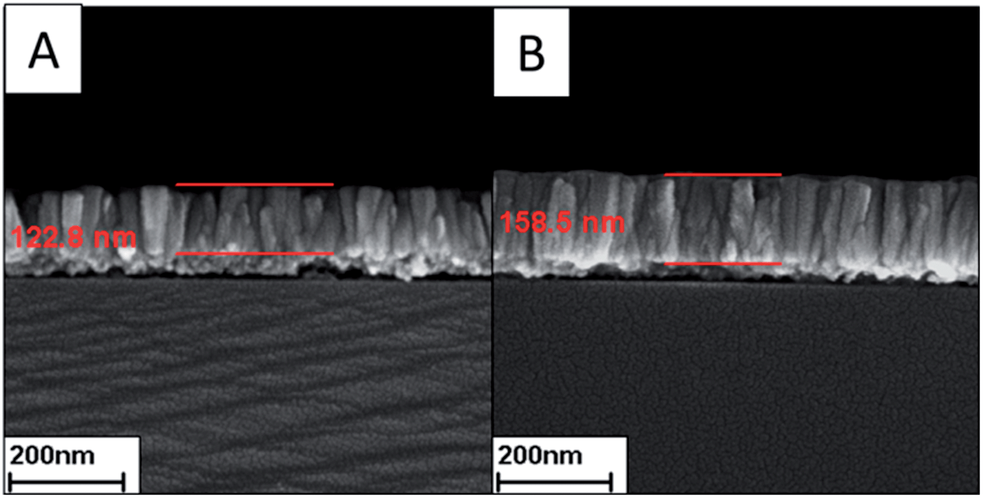
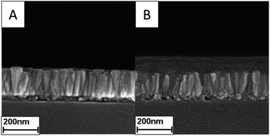
At a growth time of 45 minutes, ZnO NRs have not yet formed the expected nanostructure. Therefore, we infer that although the nanorods have formed some surface morphology at a growth time of 45 minutes, its effect is not strong enough to enhance the device's performance. At a growth time of 60 minutes, 75 minutes, and 90 minutes, ZnO NRs have been formed; that is, the nanostructure they has been formed successfully. Regarding the above-mentioned growth times, the difference lies in the spacing between the rods and the length of the diameters. At a growth time of 105 minutes, the diameter of the ZnO nanorods increases so significantly that the ZnO NRs even begin to grow as a thin film. From the above, we can infer that after growth over a period of time, the ZnO NRs accelerate their growing speed horizontally. Their growth brings about shrinking of the space between the nanorods. Because of this, the chances of contact between the active layer and the ZnO electron transport layer are reduced. The reduction brings a negative effect with regard to improving the device performance. As a result, ZnO NRs that grew for a long period of time do not function well on the polymer solar cell. The key is whether the active layer can fill into the space between the nanorods, and this is also the reason why the device performance with a growth time of 90 minutes is worse than that with 60 minutes and 75 minutes; nevertheless, we could not tell much of a difference from the SEM top view. Hence, we also analyzed the SEM cross-section view and exhibited the result in Fig. 4. We can see from Fig. 3 and 4 that despite the fact that not much of a difference exists when looking into the SEM top view, the SEM cross-section shows that the length of the ZnO nanorods is different. The ZnO nanorod diameter and coverage with respect to growing time is shown in Fig. S1 and Table S1.† The XRD pattern and Raman scattering spectrum of ZnO nanorods are shown in Fig. S2.† At the growth times of 60 minutes and 75 minutes, the length of the nanorod is 122.8 nm and 158.5 nm, respectively. Therefore, the ZnO NRs that grew at 75 minutes are more capable of transporting a carrier under the condition that the active layer can fill into the space between nanorods. To conclude, we determine that the device performs better at a growth time of 75 minutes than that of 60 minutes.
 |
| | Fig. 4 The SEM cross-section of ZnO NRs with growth time: (A) 60 min; and (B) 75 min. | |
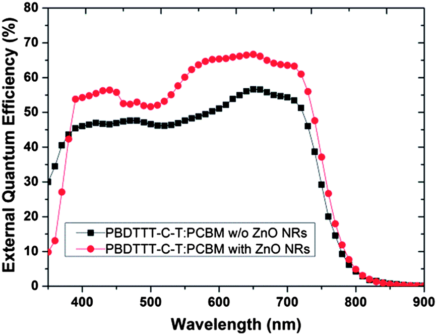
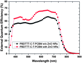
In order to find out whether ZnO NRs have operated with the active layer as expected, Fig. 5 exhibits the SEM cross-section view of the device with ZnO NRs before and after spin-coating the active layer, and Fig. 6 shows the EQE spectrum of the device with or without ZnO NRs. Fig. 5 shows that the active layer can clearly fill into the space between the nanorods. Under the condition that the active layer fills into that space, the ZnO nanorods can work as the electric transport channel to separate the electron from the hole. By decreasing the odds of electron–hole recombination, the solar energy can be converted more efficiently. Fig. 6 shows that in the wavelength of 400 nm to 800 nm, the intensity of the device with ZnO NRs is stronger than the one without ZnO NRs. In other words, the device with ZnO NRs takes the ZnO NRs as the carrier transport channel for carrying out more photoelectric current so that the PCE of the device will be enhanced. Besides, at a wavelength of 300 nm to 400 nm, the intensity of the device with the ZnO NRs is apparently weaker than that without it because the wavelength of 350 nm is the luminescence peak of ZnO. However, the above-mentioned factor does not bring too much influence on the device because the wavelength of 300 nm to 400 nm is not the main domain of the solar spectrum intensity. Furthermore, in order to apply better the ZnO NRs in the organic polymer cells, the active layer is spin-coated at different speeds. Fig. 7 shows the SEM top-view result of the spin-coating speed of the active layer with 1000 rpm, 1500 rpm, and 2000 rpm. For the devices with spin-coatings of 1000 rpm and 1500 rpm, not much of a difference exists. For the device with a spin-coating of 2000 rpm, the shape of a similar ZnO nanorod hexagonal shape can be seen. Thus, the active layer may be penetrated by the ZnO nanorods, and the device's performance is reduced.32 Therefore, controlling the spin-coating speed of the active layer is an important issue for a device with ZnO NRs.
 |
| | Fig. 5 The SEM cross-section of ZnO NRs with growth time 75 min (A) without active layer (B) with active layer. | |
 |
| | Fig. 6 The EQE spectrum of device with and without ZnO NRs in PBDTTT-C/PC71BM. | |
 |
| | Fig. 7 The SEM top view of ZnO NRs surface morphology with different active layer spin-coated speed (A) 1000 rpm (B) 1500 rpm (C) 2000 rpm (D) without active layer. | |
Next, we applied ZnO NRs on the PBDTTT-C-T/PC71BM system. According to the previous observation, we have realized that the spacing between the ZnO nanorods will affect the contact of the active layer and affect the device performance. Therefore, we set the growth time of the ZnO nanorod array at 75 minutes and compared the device performance between the devices without and with ZnO NRs, which grew at a 60 mM and 75 mM concentration, respectively. The result of the device performance and JV curve are shown in Table 2 and Fig. 8. Fig. 9 shows the SEM of the ZnO NRs that grew at a 60 mM concentration from diverse angles. Fig. 10 shows the EQE spectrum of the device without ZnO NRs and the device with ZnO NRs that grew at a 60 mM concentration. We can determine from the Table that we have successfully applied the ZnO NRs to different donor materials because the short current density of the device significantly improved after growing the ZnO NRs. The Jsc of the device without the ZnO NRs is 13.5 mA cm−2 with PCE 5.40%. The Jsc of the device with the ZnO NRs that grew at a 60 mM concentration is 17.0 mA cm−2 with a PCE of 7.34%. The Jsc of the device with the ZnO NRs that grew at a 75 mM concentration is 16.4 mA cm−2 with PCE 6.81% conversion efficiency. Fig. 8 shows that the ZnO NRs that grew at a 60 mM concentration possesses a larger spacing than do the ZnO NRs that grew at a 75 mM concentration. The result implies that more and more active layers are able to fill into the spacing to function as the electron transport channel for enhancing the effect of exciton separation. In order words, the 60 mM concentration of growth solution proves to be the better ZnO NRs morphology for a polymer solar cell than is the 75 mM concentration. In Fig. 9 EQE spectrum, we can see that because the device with ZnO NRs takes ZnO as the electron transport channel, it reduces the possibility of electron–hole recombination. As a result, the EQE spectrum intensity of the device with the ZnO nanorod array is better than the one without ZnO NRs. Similarly, under the influence of ZnO emission around a wavelength of 340 nm, the device with ZnO NRs performs with a weaker EQE spectrum intensity than does the device without ZnO NRs in between the wavelengths of 300 nm to 400 nm.
Table 2 The PV parameters of devices PBDTTT-C-T/PC71BM without ZnO NRs and with ZnO NRs of different growth concentration
| Concentration/mM |
PCE (%) |
J
sc/mA cm−2 |
V
oc/V |
FF (%) |
R
s/Ω cm2 |
R
sh/Ω cm2 |
| w/o ZnO NRs |
5.40 |
13.5 |
0.788 |
50.55 |
8.0 |
261.18 |
| 60 |
7.34 |
17.0 |
0.746 |
57.93 |
4.5 |
309.54 |
| 75 |
6.81 |
16.4 |
0.739 |
56.05 |
4.3 |
268.02 |
 |
| | Fig. 8 The J–V characteristics under AM 1.5 G solar illumination with different ZnO NRs growth concentration. | |
 |
| | Fig. 9 The SEM of ZnO NRs morphology with different side (A) cross section (B) cross section with active layer (C) top view (D) 45 degree view. | |
 |
| | Fig. 10 The EQE spectrum of the device with and without ZnO NRs in PBDTTT-C-T/PC71BM. | |
We also compare the performance of the device PBDTTT-C-T/PC71BM with the ZnO sol–gel seed layer, the ZnO nanoparticles and the ZnO nanorods. As shown in Table 3, the performance of the device with the ZnO nanoparticles is similar to the one with the ZnO seed layer. As in other work, the morphology of the ZnO seed layer in Fig. 3A is similar to that of the ZnO nanoparticles.33 Thus, in the ZnO seed layer and nanoparticles, the active layer just covers this buffer layer. In contrast, with the ZnO NRs, the active layer can fill more into the space and thus have more contact area.
Table 3 The PV parameters of devices PBDTTT-C-T/PC71BM with ZnO seed layer, nanoparticle and nanorod
| Status (PBDTTT-C-T/PCBM) |
PCE (%) |
J
sc/mA cm−2 |
V
oc/V |
FF (%) |
R
s/Ω cm2 |
R
sh/Ω cm2 |
| ZnO seed layer |
5.40 |
13.5 |
0.788 |
50.55 |
8.0 |
261.18 |
| ZnO nanoparticles |
5.95 |
14.4 |
0.766 |
54.10 |
7.8 |
348.16 |
| ZnO nanorod |
7.34 |
17.0 |
0.746 |
57.93 |
4.5 |
309.54 |
Conclusions
We applied ZnO NRs to low-bandgap polymer solar cells by controlling the growth time and concentration of the growth solution. By adopting ZnO NRs as an electron transport channel, the possibility of electron–hole recombination is greatly reduced because we have successfully filled the active layer into the spacing of ZnO NRs. This also helps to increase the device's Jsc and PCE. Moreover, we also applied the ZnO nanorod structure to different systems. In the PBDTTT-C/PC71BM system, the Jsc and PCE raise from 12.1 mA cm−2 to 15.9 mA cm−2 and from 4.76% to 6.07%, respectively. In the PBDTTT-C-T/PC71BM system, Jsc and PCE raise from 13.5 mA cm−2 to 17.0 mA cm−2 and from 5.40% to 7.34%, respectively. Based on the above result, we have successfully discovered a potentially universal and efficient way to enhance the device performance.
Acknowledgements
This work was supported by the National Science Council, Taiwan, Republic of China with the project numbers: NSC 100-2923-E-002-005-MY3 and NSC 102-3113-P-002-027.
Notes and references
- F. C. Krebs, Sol. Energy Mater. Sol. Cells, 2009, 93, 394–412 CrossRef CAS PubMed.
- B. C. Thompson and J. M. J. Frechet, Angew. Chem., Int. Ed., 2008, 47, 58–77 CrossRef CAS PubMed.
- C. J. Brabec and J. R. Durrant, MRS Bull., 2008, 33, 670–675 CrossRef CAS.
- M. R. Lilliedal, A. J. Medford, M. V. Madsen, K. Norrman and F. C. Krebs, Sol. Energy Mater. Sol. Cells, 2010, 94, 2018–2031 CrossRef CAS PubMed.
- J. Subbiah, C. M. Amb, I. Irfan, Y. Gao, J. R. Reynolds and F. So, ACS Appl. Mater. Interfaces, 2012, 4(2), 866–870 CAS.
- K. S. Chen, Y. Zhang, H. L. Yip, Y. Sun, J. A. Davies, C. Ting, C. P. Chen and A. K. Y. Jen, Org. Electron., 2011, 12(5), 794–801 CrossRef CAS PubMed.
- T. Y. Chu, S. Alem, S. W. Tsang and S. C. Tse, Appl. Phys. Lett., 2011, 98, 253301 CrossRef.
- L.-M. Chen, Z. Hong, G. Li and Y. Yang, Adv. Mater., 2009, 21, 1434–1449 CrossRef CAS.
- J. S. Huang, C. Y. Chou and C. F. Lin, IEEE Electron Device Lett., 2010, 31, 332–334 CrossRef CAS.
- M. S. White, D. C. Olson, S. E. Shaheen, N. Kopidakis and D. S. Ginley, Appl. Phys. Lett., 2006, 89, 143517 CrossRef.
- P. C. Yang, J. Y. Sun, S. Y. Ma, Y. M. Shen, Y. H. Lin, C. P. Chen and C. F. Lin, Sol. Energy Mater. Sol. Cells, 2012, 98, 351–356 CrossRef CAS PubMed.
- J. S. Kim, Y. Lee, J. H. Lee, J. H. Park, J. K. Kim and K. Cho, Adv. Mater., 2010, 22, 1355–1360 CrossRef CAS PubMed.
- J. C. Wang, C. Y. Lu, J. L. Hsu, M. K. Lee, Y. R. Hong, T. P. Perng, S. F. Horng and H. F. Meng, J. Mater. Chem., 2011, 21, 5723 RSC.
- C. S. Kim, S. S. Lee, E. D. Gomez, J. B. Kim and Y. L. Loo, Appl. Phys. Lett., 2009, 94, 113302 CrossRef.
- Y. F. Li, Acc. Chem. Res., 2012, 45(5), 723–733 CrossRef CAS PubMed.
- L. Huo, S. Zhang, X. Guo, F. Xu, Y. F. Li and J. Hou, Angew. Chem., Int. Ed., 2011, 50, 9697–9702 CrossRef CAS PubMed.
- C. Winder and N. S. Sariciftci, J. Mater. Chem., 2004, 14, 1077–1086 RSC.
- E. Bundgaard and F. C. Krebs, Sol. Energy Mater. Sol. Cells, 2007, 91, 954–985 CrossRef CAS PubMed.
- V. D. Mihailetchi, H. Xie, B. D. Boer, L. M. Popescu, J. C. Hummelen, P. W. M. Blom and L. J. A. Koster, Appl. Phys. Lett., 2006, 89, 012107 CrossRef.
- T. Y. Chua, S. W. Tsanga, J. Zhoua, P. G. Verlya, J. Lua, S. Beaupréb, M. Leclercb and Y. Taoa, Sol. Energy Mater. Sol. Cells, 2012, 96, 155–159 CrossRef PubMed.
- E. M. C. Fortunato, P. M. C. Barquinha, A. C. M. B. G. Pimentel, A. M. F. Gonçalves, A. J. S. Marques, R. F. P. Martins and L. M. N. Pereira, Appl. Phys. Lett., 2004, 85, 2541 CrossRef CAS.
- Y. Sun, J. H. Seo, C. J. Takacs, J. Seifter and A. J. Heeger, Adv. Mater., 2011, 23, 1679–1683 CrossRef CAS PubMed.
- A. K. K. Kyaw, X. W. Sun, C. Y. Jiang, G. Q. Lo1, D. W. Zhao and D. L. Kwong, Appl. Phys. Lett., 2008, 93, 221107 CrossRef.
- K. Takanezawa, K. Hirota, Q. S. Wei, K. Tajima and K. Hashimoto, J. Phys. Chem. C, 2007, 111(19), 7218–7223 CAS.
- K. Takanezawa, K. Tajima and K. Hashimoto, Appl. Phys. Lett., 2008, 93, 063308 CrossRef.
- G. Li, V. Shrotriya, J. Huang, Y. Yao, T. Moriarty, K. Emery and Y. Yang, Nat. Mater., 2005, 4, 864–868 CrossRef CAS.
- G. Namkoong, J. Kongb, M. Samsona, I. W. Hwangd and K. Lee, Org. Electron., 2013, 14, 74–79 CrossRef CAS PubMed.
- S. H. Kao, Z. L. Tseng, P. Y. Ho, C. Y. Kao, S. Thiyagu and C. F. Lin, J. Mater. Chem. A, 2013, 1, 14641–14648 CAS.
- M. Guo, P. Diao and S. Cai, J. Solid State Chem., 2005, 178, 1864–1873 CrossRef CAS PubMed.
- H. Hoppe and N. S. Sariciftci, J. Mater. Res., 2004, 19, 7 CrossRef.
- J. Y. Sun, W. H. Tseng, S. Lan, S. H. Lin, P. C. Yang, C. I. Wua and C. F. Lin, Sol. Energy Mater. Sol. Cells, 2013, 109, 178–184 CrossRef CAS PubMed.
- C. S. Chen, P. C. Yang, Y. M. Shen, S. Y. Ma, S. C. Shiu, S. C. Hung, S. H. Lin and C. F. Lin, Sol. Energy Mater. Sol. Cells, 2012, 101, 180–185 CrossRef CAS PubMed.
- M. AzizIbrahem, H. Y. Wei, M. H. Tsai, K. C. Ho, J. J. Shyue and C. W. Chu, Sol. Energy Mater. Sol. Cells, 2013, 108, 156–163 CrossRef PubMed.
Footnote |
| † Electronic supplementary information (ESI) available. See DOI: 10.1039/c3nr04418a |
|
| This journal is © The Royal Society of Chemistry 2014 |
Click here to see how this site uses Cookies. View our privacy policy here.