
ZnS anisotropic nanocrystals using a one-pot low temperature synthesis†
Aude
Buffard
a,
Brice
Nadal
b,
Hadrien
Heuclin
b,
Gilles
Patriarche
c and
Benoit
Dubertret
*a
aLaboratoire de Physique et d'Étude des Matériaux, PSL Research University, CNRS UMR 8213, Sorbonne Universités UPMC Univ Paris 06, ESPCI ParisTech, 10 rue Vauquelin, 75005 Paris, France. E-mail: benoit.dubertret@espci.fr
bNexdot, 10 rue Vauquelin, 75005 Paris, France
cLaboratoire de Photonique et Nanostructures, CNRS, Route de Nozay 91460, Marcoussis, France
First published on 16th October 2014
Abstract
We report a simple, low temperature and scalable synthesis of wurtzite ZnS anisotropic nanocrystals performed under air. The reaction between a zinc salt (nitrate or chloride) with thioacetamide and amines at 60 °C yields ZnS nanoplatelets or nanowires absorbing in the ultra-violet region with a full width at half maximum between 11 nm and 15 nm.
During the past two decades, the synthesis of colloidal semiconductor nanocrystals (NCs) has seen an impressive progress motivated by the possibility of tuning the electronic and optical properties of these nano-objects, thanks to quantum confinement effects. These physical properties are the key issues in many applications such as LEDs,1 biolabeling, biosensing2,3 and solar cells.4 The group II–VI semiconducting NCs have been mainly studied and a lot of chemical approaches have been used to synthesize 0D spherical quantum dots,5 1D quantum rods6 and 2D nanoplatelets7 since the first synthesis of monodisperse CdE (E = S, Se, Te) in 1993.5 Zinc sulfide has been used for the growth of shells on other nanocrystals8 because it improves the fluorescence quantum yield and enhances the resistance against photobleaching thanks to its large band gap (3.91 eV at 300 K in the hexagonal structure). Contrary to Cd-based NCs, ZnS exhibits very low toxicity. In addition, its band gap in the ultraviolet range makes it a promising material for new applications such as ultraviolet sensors.9 A few studies have been conducted on the synthesis of ZnS nanocrystals or nanorods, mostly by Hyeon's group at high temperature.10,11 ZnS nanosheets have been obtained using different synthetic routes,9 including the thermal evaporation method of ZnS powder,12 or by colloidal synthesis at high temperatures (160 °C to 280 °C).13,14 Low temperature syntheses of ZnS anisotropic nanocrystals would allow the simplification of the implementation of the synthesis and an easy transition to a large-scale production.
Studies on the low temperature synthesis of nanocrystals have already been published. For example, nanocrystals of CdS, Ag2S or Bi2S3 have been obtained.15,16 Hyeon's group published the synthesis of CdSe, CdTe and CdS nanoplatelets (NPLs) using CdCl2 as the cadmium precursor and a chalcogene with alkylamines as solvents.17 They hypothesized a lamellar mechanism which was supported by Buhro's group for the synthesis of CdSe nanobelts.18 O'Brien's group reported the synthesis of ZnS quantum dots and nanorods.19 Our group reported the synthesis of ZnS NPLs starting from CdS NPLs via a cation-exchange mechanism.20 In this paper, we report a simple, low temperature and scalable route to synthesize ZnS anisotropic nanocrystals taking advantage of previous observations of Mahler et al. for the growth of CdS shells on CdSe NPLs at low temperature.21 The synthesis was carried out in air without taking special precautions for precursor use. This reaction relies on the slow generation of H2S gas consecutively to the reaction between thioacetamide and primary amines, as described by the group of Ozin.22 One population of nanowires and one population of NPLs absorbing respectively at 256 nm and 282 nm could be synthesized, isolated and characterized. They present narrow excitonic features with a full width at half maximum (FWHM) between 11 and 15 nm. TEM microscopy confirmed the platelet-like morphology for NPLs absorbing at 256 nm. Moreover, the influence of a mixture of amines on this synthesis has been studied.
As mentioned in the introduction, the reaction between primary amines and thioamides leads to the formation of amidines via generation of H2S gas.22 In our case, we used octylamine or oleylamine as the primary amine (Scheme 1). The H2S generated can then react with metal salts to produce metal sulfide nanocrystals.
 | ||
| Scheme 1 Reaction between thioacetamide and an amine leading to the formation of hydrogen sulfide and strategies to synthesize ZnS NCs. | ||
In a first synthesis, we mixed thioacetamide, octylamine and zinc nitrate in chloroform at 60 °C for 3 h (Route A in Scheme 1). An absorption spectrum of the crude mixture (Fig. S1A in the ESI†) showed the presence of ZnS nanocrystals as well as a large peak at about 265 nm that we attributed to sulfur-containing impurities. Indeed, mixing thioacetamide with amines only and heating this solution at 60 °C for 3 h led to the same large peak at 265 nm in the absorption spectrum, confirming our hypothesis (Fig. S1E, ESI†). ZnS nanocrystals were isolated by precipitation with ethanol (sulfur-containing impurities remained in the supernatant as evidenced by the absorbance spectrum in Fig. S1B, ESI†). The nanocrystals were dispersible in chloroform and were washed twice more and finally suspended in hexane. As we can see in Fig. 1A, the maximum of the excitonic peak in the absorption spectrum is 282 nm. Compared to bulk ZnS (340 nm) the maximum of the excitonic peak in absorption is blue-shifted. The FWHM is about 14 nm.
 | ||
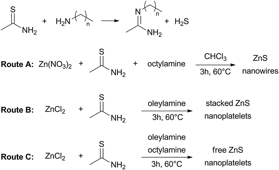
| Fig. 1 (A) Absorption spectrum (B), (C) TEM image and (D) HAADF-TEM image with corresponding zoom showing crystal planes of nanowires synthesized by route A. | ||
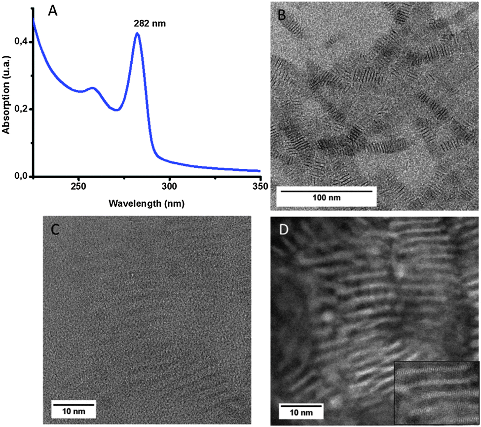
Fig. 1B–D show TEM and HAADF-TEM images of a typical sample of ZnS nanowires with an absorption peak at 282 nm. The inset in Fig. 1D allows seeing the crystal planes of the nanocrystals. On average the nanowires are 10 nm long and 1.3 nm thick. During the TEM experiment, a 25° tilt of the grid was performed in order to confirm that we had obtained nanowires and not nanoplatelets (see Fig. S4, ESI†). No projection of the width could be seen on the TEM images thus confirming the wire-like morphology of the nanocrystals. On the TEM images, we found that the spacing between stacked nanowires is about 2 nm. We attributed this value to the presence of octylamine ligands on the surface of the nanocrystals (see Fig. 2A). This distance was confirmed by low angle DRX measurements (Fig. 2B) where we can see the harmonic peaks named d*, d*/2, d*/3 and which was 3 nm thanks to Bragg's law (eqn S1 in ESI†). This value corresponds in total to two ligands and one nanowire. The distance between nanowires is thus about 1.7 nm (since one nanowire is 1.3 nm thick on TEM), which is in good agreement with the measurement obtained using TEM. Using Tanford's formula,23 we calculated the theoretical distance between each nanocrystal considering that octylamine was the only ligand. The length of an octylamine chain can be approximated using: lmax = 1.5 + 1.265 nC with lmax being the length of the ligand with maximum extension of the hydrocarbon chain in Å and nC the number of carbon atoms in the ligand. It predicts a length of 1.3 nm for octylamine. If we consider that there are two ligands between each nanowire, we obtain a value of 2.6 nm for the space between two nanowires. This suggests that the octylamine chains are slightly interdigitated as shown in Fig. 2A.
 | ||
| Fig. 2 (A) Schematic representation of two nanowires. (B) Low angle XRD of the same ZnS anisotropic nanocrystals with a wavelength of the source λCu-kα = 1.54 Å. | ||
We then investigated different ratios of reactants to see if other morphologies or thicknesses could be obtained. At first we tried to keep the ratio octylamine/thioacetamide constant and vary the ratio thioacetamide/Zn. We observed no influence of the increase or decrease of the quantity of Zn on the maximum wavelength on absorption spectrum but the nanocrystals are more agglomerated (see Fig. S2A in the ESI†). When the ratio octylamine/thioacetamide was varied keeping the quantity of Zn constant, no defined nanocrystals could be obtained. In contrast, only aggregates could be seen by TEM analysis (see Fig. S2B in the ESI†). We finally chose to synthesize our nanowires with ratios octylamine/thioacetamide = 7.5 and thioacetamide/Zn = 8.7.
We then tried to extend the synthesis of ZnS anisotropic nanocrystals to nanoplatelets while maintaining a low temperature. In 2009, Hyeon's group developed a synthesis method to produce CdSe, CdTe and CdS NPLs using CdCl2 as the cadmium precursor.17 They hypothesized that the formation of NPLs was possible thanks to a lamellar mechanism with the cadmium precursor [(RNH2)2CdCl2] as a soft template to induce 2D growth. We have adapted this reaction in order to synthesize ZnS NPLs (Route B in Scheme 1). We heated thioacetamide, oleylamine and zinc chloride for 3 h at 60 °C. Oleylamine plays the role of both the solvent and the ligand. NPLs were washed with ethanol as the non-solvent and chloroform as the solvent. The pale yellow supernatant was discarded after observing no presence of a defined absorption peak on the spectrum and the white precipitate was washed twice and finally suspended in hexane.
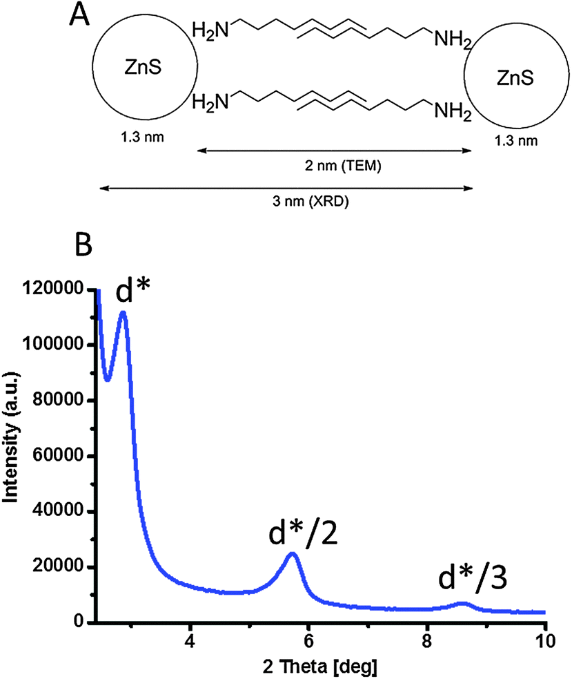
In the end we obtain a white viscous solution. As we can see on the UV-visible spectrum (Fig. 3A), the maximum of the excitonic peak in absorption is at 256 nm which is blue-shifted compared to previously synthesized ZnS NPLs. The FWHM of the absorption maximum peak is about 15 nm. Fig. 3B shows a TEM image of these ZnS NPLs. They are closely packed together in a superlattice type organization. The distance between each NPL is around 1.8 nm (determined by TEM). The TEM image shows NPLs with very different lateral sizes despite the purification process.
 | ||
| Fig. 3 (A) Absorption spectrum (B) TEM images of the ZnS NPLs synthesized via route B. (C) Absorption spectrum (D) TEM images and corresponding zoom and FFT of the free standing ZnS NPLs synthesized via route C. | ||
Hyeon's group suggested that a combination of two amines with different backbones allowed the synthesis of individual nanosheets.17 We applied this method to the population of NPLs emitting at 256 nm. We used in this case a mixture of octylamine and oleylamine (Route C in Scheme 1). Fig. 3C shows the absorption of the NPLs synthesized using this method. We can see that the same population is obtained but the FWHM is thinner (11 nm instead of 15 nm). However, TEM images (Fig. 3D) show that the NPLs are not stacked together but are well dispersed and crystalline. This can also explain the difference in FWHM between the two syntheses. It is yet unclear whether the sole combination of two different amines or the combination of a rigid and a flexible chain allow the separation of the NPLs.
The ZnS nanowires or nanoplatelets obtained via the different routes (A or B/C) are in the wurtzite structure as shown by the XRD diffractograms (Fig. 4).
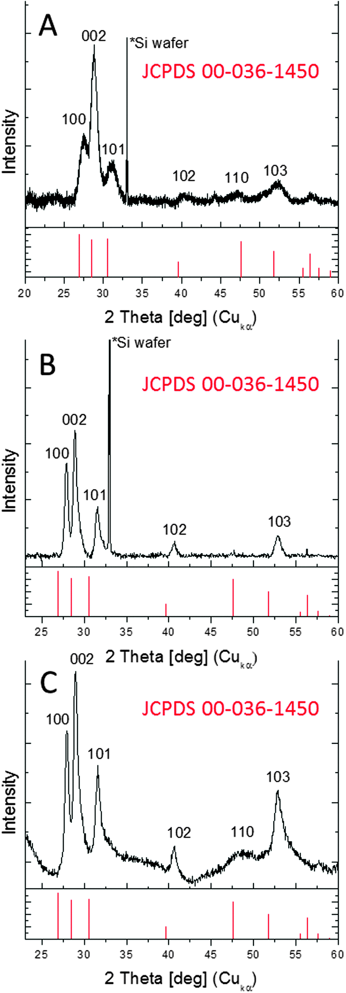 | ||
| Fig. 4 (A) XRD diffractograms of nanowires obtained via route A. (B) XRD diffractograms of nanoplatelets obtained via route B and (C) obtained via route C. | ||
In view of applications in devices, a high quantity of nanocrystals may be required. In order to test the robustness of our protocols, reactions A and B have been scaled up to 1 g of the zinc precursor. Fig. S3 in the ESI† shows that both syntheses are reproducible even in large quantities and produce good quality nanocrystals. This opens the way to even larger reaction volumes. So far, no photoluminescence could be detected for our nanocrystals. However, this does not discard our materials for use in photodetectors.
In conclusion, we have developed two syntheses in order to obtain two different morphologies of ZnS nanocrystals absorbing in the ultraviolet region. A first synthesis yields ZnS nanowires while a second one allows obtaining ZnS nanoplatelets (stacked or not). Both syntheses could be performed at low temperature and under air and could be easily scaled up to 1 gram of precursor so far. The easy, reproducible and scalable preparation of these anisotropic nanocrystals should permit applications in devices.
Experimental
Route A synthesis of ZnS nanowires with zinc nitrate
65 mg of thioacetamide (0.87 mmol) and 1.08 mL of octylamine (6.5 mmol) were mixed with 4 mL of chloroform in a vial. 500 μL of a solution of zinc nitrate at 0.2 M (0.1 mmol) in ethanol was added. The vial was put in the oven for 3 h at 60 °C. After 3 h, ZnS nanowires were precipitated with ethanol and redispersed in chloroform. This cycle of centrifugation/dispersion was repeated 3 times then the anisotropic nanocrystals were dispersed in hexane.Route B synthesis of ZnS nanoplatelets with zinc chloride and oleylamine
40 mg of zinc chloride (0.29 mmol) were dissolved in 2 mL of oleylamine and injected into a vial containing a solution of 59 mg of thioacetamide (0.78 mmol) and 1 mL of oleylamine. The vial was put in the oven for 3 h at 60 °C. After 3 h, ZnS nanoplatelets were precipitated with ethanol and redispersed in chloroform. This cycle of centrifugation/dispersion was repeated 3 times and then the nanoplatelets were dispersed in hexane.Route C synthesis of ZnS nanoplatelets with zinc chloride and oleylamine–octylamine mixture
The same protocol as route B was used but by replacing oleylamine by a mixture of oleylamine and octylamine (50/50 v/v).Acknowledgements
The authors thank the ANR (Agence Nationale de la Recherche) and the CNRS (Centre National de la Recherche Scientifique) for funding.Notes and references
- Z. Tan, F. Zhang, T. Zhu, J. Xu, A. Y. Wang, J. D. Dixon, L. Li, Q. Zhang, S. E. Mohney and J. Ruzyllo, Nano Lett., 2007, 7, 3803–3807 CrossRef CAS PubMed.
- A. P. Alivisatos, W. Gu and C. Larabell, Annu. Rev. Biomed. Eng., 2005, 7, 55–76 CrossRef CAS PubMed.
- I. L. Medintz, H. T. Uyeda, E. R. Goldman and H. Mattoussi, Nat. Mater., 2005, 4, 435–446 CrossRef CAS PubMed.
- K. Ij and E. Sargent, ACS Nano, 2013, 5, 8506–8514 Search PubMed.
- C. Murray, D. Norris and M. Bawendi, J. Am. Chem. Soc., 1993, 115, 8706–8715 CrossRef CAS.
- X. Peng, L. Manna, W. Yang, J. Wickham, E. Scher, A. Kadavanich and A. P. Alivisatos, Nature, 2000, 404, 59–61 CrossRef CAS PubMed.
- S. Ithurria and B. Dubertret, J. Am. Chem. Soc., 2008, 130, 16504–16505 CrossRef CAS PubMed.
- M. A. Hines and P. Guyot-sionnest, J. Phys. Chem., 1996, 100, 468–471 CrossRef CAS.
- X. Fang, T. Zhai, U. K. Gautam, L. Li, L. Wu, Y. Bando and D. Golberg, Prog. Mater. Sci., 2011, 56, 175–287 CrossRef CAS PubMed.
- J. Joo, H. Bin Na, T. Yu, J. H. Yu, Y. W. Kim, F. Wu, J. Z. Zhang and T. Hyeon, J. Am. Chem. Soc., 2003, 125, 11100–11105 CrossRef CAS PubMed.
- J. H. Yu, J. Joo, H. M. Park, S.-I. Baik, Y. W. Kim, S. C. Kim and T. Hyeon, J. Am. Chem. Soc., 2005, 127, 5662–5670 CrossRef CAS PubMed.
- X.-S. Fang, C.-H. Ye, X.-S. Peng, Y.-H. Wang, Y.-C. Wu and L.-D. Zhang, J. Cryst. Growth, 2004, 263, 263–268 CrossRef CAS PubMed.
- S.-O. Yu and M. Yoshimura, Adv. Mater., 2002, 14, 296–300 CrossRef CAS.
- N. S. Karan, S. Sarkar, D. D. Sarma, P. Kundu, N. Ravishankar and N. Pradhan, J. Am. Chem. Soc., 2011, 133, 1666–1669 CrossRef CAS PubMed.
- N. Pradhan and S. Efrima, J. Am. Chem. Soc., 2003, 125, 2050–2051 CrossRef CAS PubMed.
- H. Zhang, B. Hyun, F. Wise and R. Robinson, Nano Lett., 2012, 12, 5856–5860 CrossRef CAS PubMed.
- J. S. Son, X.-D. Wen, J. Joo, J. Chae, S.-I. Baek, K. Park, J. H. Kim, K. An, J. H. Yu, S. G. Kwon, S.-H. Choi, Z. Wang, Y.-W. Kim, Y. Kuk, R. Hoffmann and T. Hyeon, Angew. Chem., Int. Ed., 2009, 48, 6861–6864 CrossRef CAS PubMed.
- Y.-H. Liu, V. L. Wayman, P. C. Gibbons, R. A. Loomis and W. E. Buhro, Nano Lett., 2010, 10, 352–357 CrossRef CAS PubMed.
- S. Daniels, P. Christian and P. O'brien, J. Exp. Nanosci., 2006, 1, 97–102 CrossRef CAS.
- C. Bouet, D. Laufer, B. Mahler, B. Nadal, H. Heuclin, S. Pedetti, G. Patriarche and B. Dubertret, Chem. Mater., 2014, 26, 3002–3008 CrossRef CAS.
- B. Mahler, B. Nadal, C. Bouet, G. Patriarche and B. Dubertret, J. Am. Chem. Soc., 2012, 134, 18591–18598 CrossRef CAS PubMed.
- J. W. Thomson, K. Nagashima, P. M. Macdonald and G. A. Ozin, J. Am. Chem. Soc., 2011, 133, 5036–5041 CrossRef CAS PubMed.
- C. Tanford, J. Phys. Chem., 1972, 76, 3020–3024 CrossRef CAS.
Footnote |
| † Electronic supplementary information (ESI) available: Additional TEM images and absorbance spectrum. See DOI: 10.1039/c4nj01482k |
| This journal is © The Royal Society of Chemistry and the Centre National de la Recherche Scientifique 2015 |