
Vividly colorful hybrid perovskite solar cells by doctor-blade coating with perovskite photonic nanostructures†
Yehao
Deng
,
Qi
Wang
,
Yongbo
Yuan
and
Jinsong
Huang
*
Department of Mechanical and Materials Engineering, University of Nebraska-Lincoln, Lincoln, Nebraska 68588-0656, USA. E-mail: jhuang2@unl.edu
First published on 6th August 2015
Abstract
The colors of solar cells are very important when adopting them for future indoor and outdoor light energy harvesting devices with smart designs. Here we report the formation of vividly colorful hybrid organometal trihalide perovskite solar cells by a low-cost and scalable doctor-blade coating method. The perovskite films have a combination of a hundred micrometer size large domain structure and a concentric ring photonics structure in each domain which generates the vivid color. The convection during precursor solution drying in the doctor-blade coating process has been found to be responsible for the formation of the large domains and the coffee-ring like perovskite photonic structures after solvent drying, whose periodicity can be well tuned by the substrate temperature and the precursor solution concentration. Both the perovskite films and the finished devices are very colorful, and the efficiency of the vividly colorful solar cells is close to the optimized doctor-blade coated perovskite solar cell.
Conceptual insightsSolar cells are a promising technology to replace fossil fuels and become one of the major energy sources globally. Among their advantageous properties, the color of organic and hybrid solar cells has an important impact on their adoption by customers for their niche applications, for instance in building-integrated photovoltaic (BIPV) materials and portable chargers. The color and semi-transparency of these solar cells add a decorative value to these third generation solar cells in addition to the energy generated. The pioneering work on colorful perovskite solar cells by Snaith and co-workers (Nano Lett., 2015, 15(3), 1698–1702) inherited a concept from organic solar cells in which the color was achieved by the incomplete absorption of visible light. Here we present a completely new mechanism to achieve vividly colorful solar cells using a spontaneously generated photonic nanostructure during doctor-blade coating, which is a scalable fabrication process for large area colorful solar cell manufacturing. These colorful solar cells are also surprisingly efficient. Our analysis shows that only perovskite based colourful solar cells may have a high efficiency due to their unique defect physics, although such photonic structures may form in different material systems. |
As one of the most important “selling points” of organic solar cells, the unique tunable colors of organic solar cells are recognized to be as important as their power conversion efficiency (PCE) for building-integrated photovoltaic (BIPV) applications.1 The most efficient solar cells are always black in order to absorb as much light as possible, but colorful solar cells can not only provide electricity for our daily needs, but can also act as a decoration for our living surroundings, including clothing, vehicles and buildings.2,3 Though colorful solar cells have a relatively lower PCE because they allow some of the spectrum of visible light to pass through and/or be reflected to have a colorful appearance, there have been ongoing endeavors to fabricate colorful solar cells, particularly those made of semiconducting polymers.4–11 However, there are still issues with the many reported colorful solar cells that limit their application potential. First, the fabrication cost and time would increase a lot because the one or two dimensional photonic structures for their color appearance are often processed by expensive and time-consuming high vacuum thermal evaporation or lithography methods.5,12,13 Second, the PCE of colorful solar cells are generally well below that of their regular black counterparts because of the much thinner photoactive layer for devices with a see-through mode or an increased device resistance and/or carrier recombination due to the complicated photonic structure.9,11 Here, we report a new type of colorful solar cell based on organometal trihalide perovskite (OTP) materials formed by a low cost doctor-blading method, which could reverse the aforementioned disadvantages. The two dimensional photonic structures on the OTP films form spontaneously and instantly by Rayleigh–Bénard convection14–18 and the “coffee ring” effect19–24 during doctor-blade coating within 1–2 seconds in ambient conditions. The solar cell based on such an OTP film has a stabilized PCE of 12.2%, maintaining 80% of the efficiency of standard black OTP solar cells fabricated in a similar way.25 The high PCE, despite the complex photonic structure, is ascribed to the superior carrier transportation and defect physics of the OTP materials.
The process of OTP film formation by doctor-blade coating is shown in Fig. 1a. A substrate (e.g. hole transport layer coated indium tin oxide (ITO) on glass) was kept at 100–160 °C on a hotplate. A drop of CH3NH3PbI3 (MAPbI3) dissolved in N,N-dimethylformamide (DMF) solution was swiped linearly by a glass blade quickly (0.75 mm s−1) to form a thin wet film on the substrate. As the solvent evaporated, MAPbI3 crystals nucleated and grew in size and drifted along with the solvent convection driven by the temperature difference ΔT between the bottom and top surfaces of the thin layer of solution (Rayleigh–Bénard convection).14 Due to the high substrate temperature, the film dried within 1–2 seconds and left a final MAPbI3 polycrystalline film. We found that when the solution concentration was below a certain value (∼350 mg ml−1), a vividly colorful OTP film was obtained, as shown in Fig. 1c. The left image is an as-prepared OTP film, and the right image is a complete solar cell device with a thermal evaporated aluminum electrode on the top. Both photos were taken in reflection mode from the film side. Fig. 1b and d show the microstructure of the cross section and top view, respectively, of an as-prepared film, obtained by scanning electron microscopy (SEM). The films are composed of two kinds of regular patterns with different length scales: polygon domains (highlighted in purple) on the scale of 20–100 μm with their size depending on the substrate temperature, and a series of concentric rings (highlighted in red) with a thickness of ∼350 nm and a nearly equal ring-to-ring spacing in each domain. The ring space is between 2 μm and 6 μm depending on the solution concentration. The higher magnification cross section SEM image in the upper panel in Fig. 1b shows that each ring is composed of many MAPbI3 nanocrystals with an average size of around 500 nm. We found that the concentric ring structures always accompany the vivid color of the films. A low concentration of the MAPbI3 precursor solution is critical in yielding the formation of the concentric rings by doctor-blade coating. When the MAPbI3 precursor solution concentration was increased to above 350 mg ml−1, the concentric rings disappeared, and only the polygon domains were left in the film (Fig. S1(a), ESI†). The bladed films were black without the perovskite photonic structure, agreeing with our previous study.25 This highly periodic concentric ring structure on the micrometer scale works as a reflection grating in the visible light range, which splits and diffracts the reflected visible light into different directions, depending on the wavelength. The selective reflection results in a vivid colorful appearance over the whole visible light spectrum for the doctor-bladed OTP films. It is noted that similar structural color is also observed in CD/DVD disks or regular optical gratings, which contain small trenches on the micrometer/sub-micrometer scale and also interact strongly with visible light.
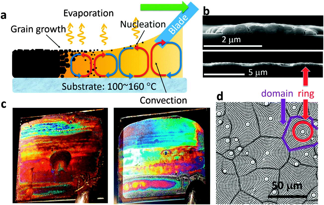 | ||
| Fig. 1 (a) An illustration of the doctor-blade coating of the organometal trihalide perovskite (OTP) films on a preheated substrate. (b) Cross section SEM images of the concentric ring structure in an as-prepared colorful OTP film. (c) Photographs of the as-prepared colorful OTP film (left) and the complete device with an aluminum electrode on top (right). Both samples were placed under 1 sun simulated illumination. (d) Plane view SEM image of the as-prepared colorful OTP film showing the polygon domains and concentric ring structure in each domain. | ||
Such spontaneous formation of the photonic structures in the OTP films is scalable to large area colorful solar cell fabrication. It is then highly interesting to learn how such patterns form and evolve. First of all, the polygon domains squeezing with each other resemble the classic Bénard cell pattern in Rayleigh–Bénard convection.15,18 As illustrated in Fig. 1a, the solution close to the substrate with higher temperature tends to flow upwards due to the buoyancy force arising from its relatively low density compared to the surrounding colder solution.18 When the hot solution reaches the top surface, its temperature decreases and it flows back to the bottom to get heated again. A number of localized convections form in this way within the thin solution films. Each convection cell tends to push others in its surroundings due to the reverse circulation direction at the edge of the cell, forming polygon patterns, as illustrated in Fig. 2a. Film formation of the OTP material in the solution is driven by the convection, and thus inherits the polygon patterns, resulting in a polygon pattern in the solid films after drying. Since the convection is driven by the temperature gradient (ΔT), changing the substrate temperature can modify the convection flow strength, and thereby change the polygon domain size. As is shown in Fig. 2b–d, when the substrate temperature increased from 100 °C to 160 °C the domain size increased from 20 μm to over 100 μm. This can be explained by the longer range convention under a higher temperature gradient. The similar pattern reported very recently by W. Nie et al.26 can also be explained by the convection because of the heated ITO substrate used in that study. In their as-prepared OTP films, the Bénard cells appeared from 130 °C with a size of ∼30 μm and increased to ∼200 μm when the temperature was increased to 190 °C.26
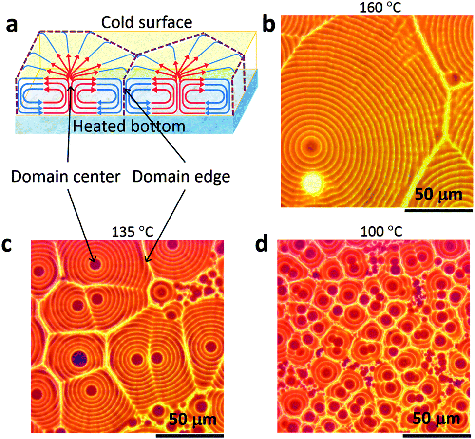 | ||
| Fig. 2 (a) An illustration of a Rayleigh–Bénard convection cell in a thin solution film driven by the temperature difference between the heated bottom and cold top surface. (b)–(d) Microscopy images of the as-prepared colorful OTP films prepared when the substrate temperature is 160 °C, 135 °C, and 100 °C, respectively. | ||
The concentric ring photonic structure within each domain can be explained by another convection mechanism, the “coffee ring effect”.19,20,22–24 Typically, the coffee ring effect occurs when a drop of solution containing nonvolatile solutes is drying on a solid surface.19 Normally the contact line between the edge of the solution droplet and the solid surface is pinned on the surface, thus during drying the solution in the interior keeps flowing to the contact line region to replenish the solvent evaporating there in order to prevent the contact line from contracting.19,23 The solutes are carried along with the outward flow to the contact line, which results in the formation a dense ring at the contact line after drying.19,23 In many cases, the contact line of a droplet contracts towards the interior through alternating pinning and de-pinning processes during solvent evaporation due to the competition between the pinning force (which tends to fix the contact line) and the surface tension of the solution (which tends to induce droplet shrinkage and thus contract the contact line).20,21 During the pinning period, as solvent is flowing to the contact line and evaporating, the solution flattens out and then the contact angle on the contact line decreases. Decreasing the contact angle increases the lateral component of the surface tension of the solution, which eventually balances the pinning force, then the contact line starts to move inward to release the lateral surface tension by shrinking the droplet to increase the contact angle, i.e. de-pinning. Once the lateral surface tension is released, the contact line is pinned again. During these pinning and de-pinning processes, the solutes (the OTP material and nanocrystals in this case) pile up along every contact line during every pinning period, forming a series of narrow concentric rings instead of one wide ring after drying, as is illustrated by the cross sectional view in Fig. 3a.22,24 To find out whether the concentric ring structure in the OTP films formed in the same manner, we “freeze” the films at different stages during drying by dropping an anti-solvent, toluene, to extract the solvent, N,N-dimethylformamide (DMF), in a very short time. Toluene can mix with DMF but cannot dissolve the OTP material, thus a drop of toluene can quickly remove DMF from the solution and prevent the film's microstructure from further evolving.27,28 The corresponding top view SEM images at different stages of film evolution are shown in Fig. 3b. They are consistent with the above description, that the rings appeared first at the edge, and then gradually developed inwards to the center of the domain. Therefore, it is concluded that the concentric ring structure causing the vivid color of the OTP films is formed by the “coffee-ring effect”. We found that by decreasing the solution concentration from 350 mg ml−1 to 180 mg ml−1 the ring spacing decreased from 6 μm to 2 μm (Fig. S1(b) and (c), ESI†), giving the flexibility to tune the periodicity of the spontaneous photonic structures in the OTP films and thus their color. This can be explained by the difference in time that is needed to reach the supersaturated conditions necessary for MAPbI3 nanocrystal formation. The nanocrystals can form by nucleation of MAPbI3 at the solution surface which provides a heterogeneous interface for easy nucleation. Since the space of the substrate on the slide glass is fixed, a lower precursor solution concentration leads to a thinner solution film when MAPbI3 crystals start to nucleate, because it needs to evaporate more solvent to reach the same supersaturation point. A thinner film experiences a faster increase in lateral surface tension due to the smaller contact angle on the contact line. Therefore, the critical point when the pinning force and lateral surface tension are balanced occurs more frequently, thus the pinning/de-pinning frequency increases, and the ring spacing decreases for the films drying from the lower MAPbI3 concentration. It should be noted that the whole process was conducted in a N2 glovebox, and thus the influence of moisture on the photonic structure was not studied here, but this could be an interesting topic for a follow up study.
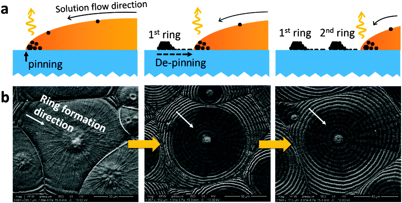 | ||
| Fig. 3 (a) An illustration of the concentric ring structure formation from the “coffee ring” effect as the contact line contracts through alternating pinning/de-pinning processes. (b) SEM images of the concentric ring structure formation at different stages “frozen” by dropping a droplet of toluene onto the wet film during drying. | ||
The vividly colorful OTP solar cells have a device structure of ITO/poly[bis(4-phenyl)(2,4,6-trimethylphenyl)amine] (PTAA)/CH3NH3PbI3/[6,6]-phenyl-C61-butyric acid methyl ester (PC60BM)/C60/2,9-dimethyl-4,7-diphenyl-1,10-phenanthroline (BCP)/aluminum, as shown in Fig. 4a.29–32 Under simulated one sun light illumination (100 mW cm−2), the device had a short circuit current (Jsc) of 18.9 mA cm−2, an open circuit voltage (Voc) of 0.89 V and a fill factor (FF) of 72% (Fig. 4b). The moderate reduction in the Jsc and Voc values compared to an optimized black OTP device fabricated by a doctor-blade coating method with Jsc of 21.8 mA cm−2 and Voc of 1.05 V25 can be explained by the smaller grain size and thus a higher grain boundary density in the colorful films that increases the charge recombination rate.33 The grain growth during the annealing process is spatially limited by the width of each ring, otherwise the grains can grow to several micrometers.29 The external quantum efficiencies (EQEs) shown in Fig. 4c were measured by tilting the angle between the incident light and the normal direction of the device plane from 0° to 70°. The integration of the EQE at 0° incident angle over the solar spectrum gives a Jsc of 18.9 mA cm−2 which is consistent with the value from the photocurrent–voltage measurement. The Jsc from 10° to 50° can still reach over 18.3 mA cm−2, but drops slightly at higher angles of 60° and 70° due to strong light reflection/scattering. This result implies that the perovskite solar cell is promising for building-integrated photovoltaic (BIPV) applications considering its good performance under a broad range of light incident angles with respect to the sun without having to rely on a complex solar tracking system. The steady photocurrent measured at the maximum power point of 0.732 V is shown in Fig. 4d. The photocurrent increased immediately to a steady value of 16.7 mA cm−2 under one sun light, giving a stabilized PCE of 12.2%. Thus the colorful device based on the photonic structured OTP layer maintains 80% of the PCE of the optimized black OTP device fabricated in a similar way which has a PCE of 15.1%.25 This result indicates that a very complexly structured OTP layer can still have a high photovoltaic performance, presumably due to the OTP layer's superior absorption and carrier transporting properties, and the much lower sensitivity to defect-related charge recombination.34
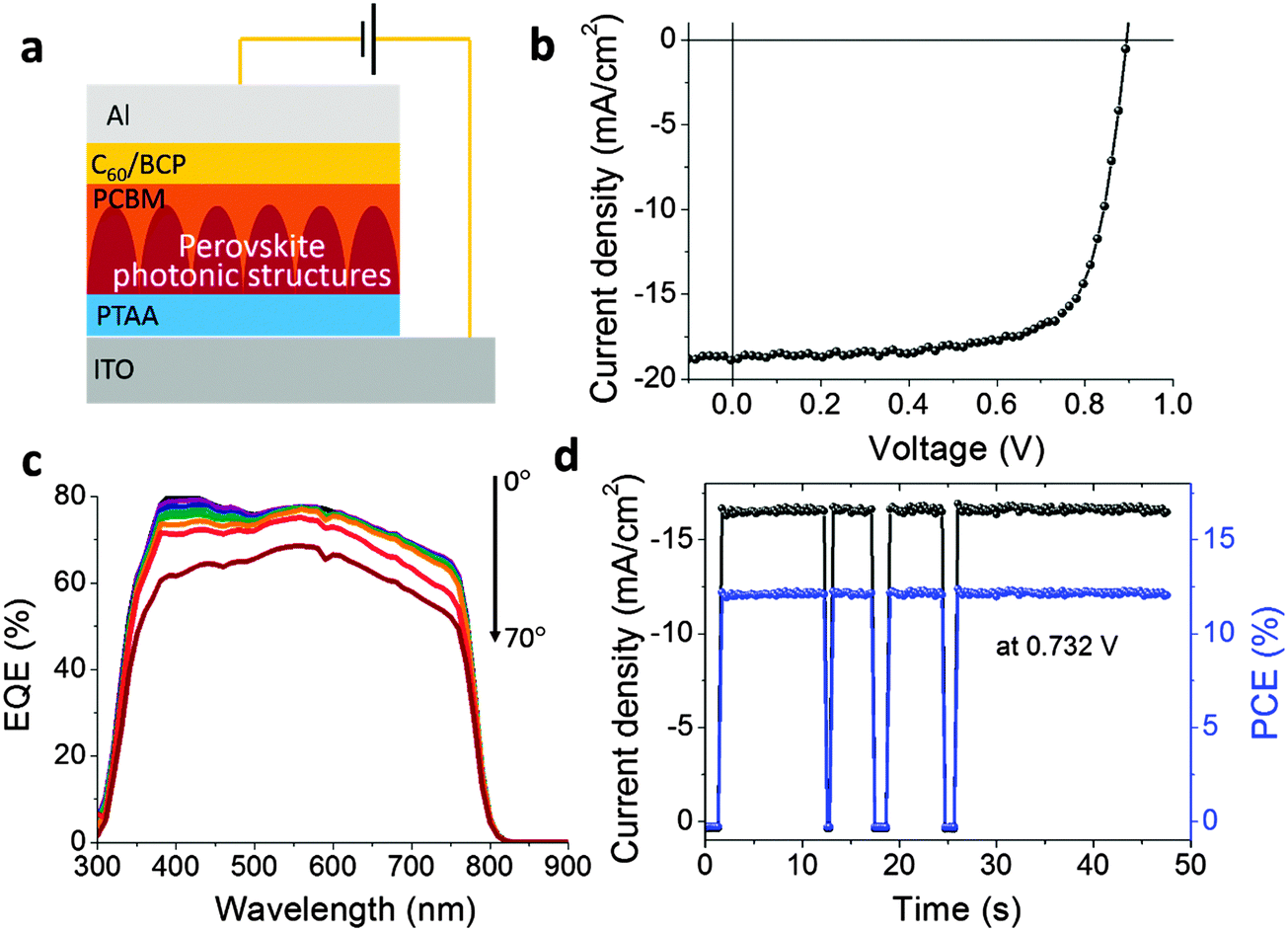 | ||
| Fig. 4 (a) An illustration of the colorful OTP solar cell device structure. (b) Photocurrent–voltage scanning of the solar cell under one sun illumination (100 mW cm−2). (c) External quantum efficiency (EQE) of the colorful OTP solar cells measured at different angles between the incident light and the normal direction of the solar cell plane. (d) Stabilized photocurrent measured at the maximum power point (0.732 V) and the PCE. | ||
In conclusion, vividly colorful OTP solar cells have been fabricated by a simple and scalable doctor-blade coating method. The photonic structures on the OTP film responsible for the vivid color appearance form spontaneously by Rayleigh–Bénard convection and the “coffee-ring effect” giving rise to a polygon domain pattern and concentric rings in each domain with near equal ring spacing. By tuning the temperature and precursor solution concentration, the domain size can be continuously tuned from 20 μm to 100 μm, and the ring spacing can be tuned from 2 μm to 6 μm, providing the ability to fine tune the photonic structure periodicity in a convenient way. This scalable, non-lithographic fabrication of photonic structured OTP films without a significant reduction in optoelectronic performance will open up a new application for OTP material based optoelectronic devices. It should be noted that this photonic structure may be reproducible in other solution processable solar cells with a similar approach, as the principle is general fluid dynamics. Nevertheless, the device efficiency of other types of colorful solar cells might be much lower. We speculate this photonic structure is uniquely applicable in OTP solar cells. This is because the relatively large layer thickness needed to form the photonic structure generally causes severe device performance degradation in many other semiconductor photovoltaic devices. The unusual defect physics of OTP materials, i.e. their tolerance to defects, enables relative high efficiency devices with these photonic structures, though there is still a minor reduction in the device efficiency. Future study can further increase the device efficiency by maintaining the photonic structure while significantly reducing the grain boundaries because the grain boundaries have been shown to be charge recombination sites in OTP solar cells.33 A semitransparent and colorful OTP solar cell is also possible based on this method because of the presence of plenty of ring-to-ring gaps in the photonic structures that light can pass through.
Materials and methods
Colorful perovskite solar cell fabrication
Indium tin oxide (ITO) coated glass substrates were cleaned with acetone, detergent, deionized water, and isopropanol successively. Before spin-coating, the substrates were treated by UV-ozone cleaner (Jelight 42) for 15 min. PTAA in 1,2-dichlorobenzene (DCB) (5 mg ml−1) was spin-coated onto the ITO substrates at 6000 rpm for 30 s and annealed in a nitrogen atmosphere at 100 °C for 10 min. Then, the PTAA covered ITO substrates were treated by argon plasma for 15 seconds and used immediately.Methylammonium iodide (CH3NH3I, MAI) and PbI2 dissolved in dimethylformamide (DMF) in a 1![[thin space (1/6-em)]](https://www.rsc.org/images/entities/char_2009.gif) :1 molar ratio were used as the doctor-blade coating precursor solution. The overall concentration ranged from 140 mg ml−1 to 540 mg ml−1. The solution (∼16 μl) was dropped onto the PTAA-covered ITO substrate on a hotplate with temperatures ranging from 100 °C to 160 °C, and swiped linearly by a glass blade at a speed of 0.75 cm s−1. The as-deposited perovskite films were then annealed at 100 °C for 60 minutes. It should be noted that the critical difference between preparing black perovskite films and colorful films is the concentration of the precursor solution. As is shown in Fig. S1 (ESI†), when the concentration of the precursor is high (e.g. 540 mg ml−1), there is no concentric ring structure in the final perovskite film, and accordingly it is not colorful. When the concentration is decreased to below 350 mg ml−1, the concentric ring structure appears, and the perovskite films become colorful. After that, 20 mg ml−1 PC60BM/DCB solution was spin-coated on top of the perovskite layer at 6000 rpm for 35 s, and the films were further thermally annealed at 100 °C for 60 minutes. All of the above experiments were conducted in a N2 glove box. Finally, C60 (20 nm), BCP (8 nm) and Al electrode (100 nm) were deposited sequentially by thermal evaporation.
:1 molar ratio were used as the doctor-blade coating precursor solution. The overall concentration ranged from 140 mg ml−1 to 540 mg ml−1. The solution (∼16 μl) was dropped onto the PTAA-covered ITO substrate on a hotplate with temperatures ranging from 100 °C to 160 °C, and swiped linearly by a glass blade at a speed of 0.75 cm s−1. The as-deposited perovskite films were then annealed at 100 °C for 60 minutes. It should be noted that the critical difference between preparing black perovskite films and colorful films is the concentration of the precursor solution. As is shown in Fig. S1 (ESI†), when the concentration of the precursor is high (e.g. 540 mg ml−1), there is no concentric ring structure in the final perovskite film, and accordingly it is not colorful. When the concentration is decreased to below 350 mg ml−1, the concentric ring structure appears, and the perovskite films become colorful. After that, 20 mg ml−1 PC60BM/DCB solution was spin-coated on top of the perovskite layer at 6000 rpm for 35 s, and the films were further thermally annealed at 100 °C for 60 minutes. All of the above experiments were conducted in a N2 glove box. Finally, C60 (20 nm), BCP (8 nm) and Al electrode (100 nm) were deposited sequentially by thermal evaporation.
Solar cell performance characterization
The solar cells' current–voltage (I–V) curves and steady photocurrent under bias were measured with a source-meter (Keithley 2400) under simulated AM 1.5G irradiation from a xenon lamp (Oriel 67005). The external quantum efficiency (EQE) was obtained with a Newport QE measurement kit. Top view and cross-section SEM was performed with a Quanta 200 FEG ESEM.Acknowledgements
We thank the financial support from Office of Naval Research (GRANT11903095) and National Science Foundation (Award ECCS-1252623).References
- A. Henemann, Renewable Energy Focus, 2008, 9, 14–19 CrossRef.
- B. Petter Jelle, C. Breivik and H. Drolsum Røkenes, Sol. Energy Mater. Sol. Cells, 2012, 100, 69–96 CrossRef CAS PubMed.
- M. B. Schubert and J. H. Werner, Mater. Today, 2006, 9, 42–50 CrossRef CAS.
- K. S. Chen, J. F. Salinas, H. L. Yip, L. Huo, J. Hou and A. K. Y. Jen, Energy Environ. Sci., 2012, 5, 9551 CAS.
- H. Park, T. Xu, J. Lee, A. Ledbetter and L. Guo, ACS Nano, 2011, 5, 7055–7060 CrossRef CAS PubMed.
- W. Yu, X. Jia, Y. Long, L. Shen, Y. Liu, W. Guo and S. Ruan, ACS Appl. Mater. Interfaces, 2015, 7, 9920–9928 CAS.
- J. Y. Lee, K. T. Lee, S. Seo and L. J. Guo, Sci. Rep., 2014, 4, 4192 Search PubMed.
- K. T. Lee, J. Y. Lee, S. Seo and L. J. Guo, Light: Sci. Appl., 2014, 3, e215 CrossRef PubMed.
- K. T. Lee, M. Fukuda, S. Joglekar and L. J. Guo, J. Mater. Chem. C, 2015, 3, 5377–5382 RSC.
- U. W. Paetzold, W. Qiu, F. Finger, J. Poortmans and D. Cheyns, Appl. Phys. Lett., 2015, 106, 173101 CrossRef PubMed.
- W. Zhang, M. Anaya, G. Lozano, M. E. Calvo, M. B. Johnston, H. Miguez and H. J. Snaith, Nano Lett., 2015, 15, 1698–1702 CrossRef CAS PubMed.
- M. A. Kats, R. Blanchard, P. Genevet and F. Capasso, Nat. Mater., 2013, 12, 20–24 CrossRef CAS PubMed.
- K. Diest, J. Dionne, M. Spain and H. Atwater, Nano Lett., 2009, 9, 2579–2583 CrossRef CAS PubMed.
- E. Bodenschatz, W. Pesch and G. Ahlers, Annu. Rev. Fluid Mech., 2000, 32, 709–778 CrossRef.
- M. Golubitsky, J. W. Swift and E. Knobloch, Physica D, 1984, 10, 249–276 CrossRef.
- T. Hartlep, A. Tilgner and F. H. Busse, Phys. Rev. Lett., 2003, 91, 064501 CrossRef CAS.
- D. C. Rapaport, Phys. Rev. E, 2006, 73, 025301 CrossRef CAS.
- A. V. Getling, Phys.-Usp., 1991, 34, 737–776 CrossRef PubMed.
- R. D. Deegan, O. Bakajin, T. F. Dupont, G. Huber, S. R. Nagel and T. A. Witten, Nature, 1997, 389, 827–829 CrossRef CAS.
- E. Adachi, A. S. Dimitrov and K. Nagayama, Langmuir, 1995, 11, 1057–1060 CrossRef CAS.
- M. E. Shanahan, Langmuir, 1995, 11, 1041–1043 CrossRef CAS.
- S. W. Hong, J. Xu, J. Xia, Z. Lin, F. Qiu and Y. Yang, Chem. Mater., 2005, 17, 6223–6226 CrossRef CAS.
- P. J. Yunker, T. Still, M. A. Lohr and A. G. Yodh, Nature, 2011, 476, 308–311 CrossRef CAS PubMed.
- W. Han and Z. Lin, Angew. Chem., 2012, 51, 1534–1546 CrossRef CAS PubMed.
- Y. Deng, E. Peng, Y. Shao, Z. Xiao, Q. Dong and J. Huang, Energy Environ. Sci., 2015, 8, 1544–1550 CAS.
- W. Nie, H. Tsai, R. Asadpour, J. C. Blancon, A. J. Neukirch, G. Gupta, J. Crochet, M. Chhowalla, S. Tretiak, M. A. Alam, H. Wang and A. D. Mohite, Science, 2015, 347, 522–525 CrossRef CAS PubMed.
- M. Xiao, F. Huang, W. Huang, Y. Dkhissi, Y. Zhu, J. Etheridge, A. Gray-Weale, U. Bach, Y. B. Cheng and L. Spiccia, Angew. Chem., Int. Ed., 2014, 126, 10056–10061 CrossRef PubMed.
- N. J. Jeon, J. H. Noh, Y. C. Kim, W. S. Yang, S. Ryu and S. I. Seok, Nat. Mater., 2014, 13, 897–903 CrossRef CAS PubMed.
- C. Bi, Q. Wang, Y. Shao, Y. Yuan, Z. Xiao and J. Huang, Nat. Commun., 2015, 6, 7747 CrossRef PubMed.
- Q. Wang, C. Bi and J. Huang, Nano Energy, 2015, 15, 275–280 CrossRef CAS PubMed.
- Q. Wang, Y. Shao, Q. Dong, Z. Xiao, Y. Yuan and J. Huang, Energy Environ. Sci., 2014, 7, 2359–2365 CAS.
- Z. Xiao, C. Bi, Y. Shao, Q. Dong, Q. Wang, Y. Yuan, C. Wang, Y. Gao and J. Huang, Energy Environ. Sci., 2014, 7, 2619–2623 CAS.
- D. W. de Quilettes, S. M. Vorpahl, S. D. Stranks, H. Nagaoka, G. E. Eperon, M. E. Ziffer, H. J. Snaith and D. S. Ginger, Science, 2015, 348, 683–686 CrossRef CAS PubMed.
- W. J. Yin, T. Shi and Y. Yan, Adv. Mater., 2014, 26, 4653–4658 CrossRef CAS PubMed.
Footnote |
| † Electronic supplementary information (ESI) available. See DOI: 10.1039/c5mh00126a |
| This journal is © The Royal Society of Chemistry 2015 |