
Multifunctional nano-accordion structures for stretchable transparent conductors†
Abhijeet
Bagal
a,
Erinn C.
Dandley
b,
Junjie
Zhao
b,
Xu A.
Zhang
a,
Christopher J.
Oldham
b,
Gregory N.
Parsons
b and
Chih-Hao
Chang
*a
aDepartment of Mechanical and Aerospace Engineering, North Carolina State University, Raleigh, North Carolina 27695, USA. E-mail: chichang@ncsu.edu
bDepartment of Chemical and Biomolecular Engineering, North Carolina State University, Raleigh, North Carolina 27695, USA
First published on 16th June 2015
Abstract
Multifunctional nano-accordion structures exhibiting a unique combination of conductivity, stretchability, and transparency are fabricated through a combination of nanolithography and atomic layer deposition. The nanostructured material demonstrated two orders-of-magnitude improvement in stretchability, repeatable electrical performance for cyclic stretching and bending, and broadband optical transmission up to 70%. The proposed experimental techniques and analytical models enable the deterministic design of nano-accordion geometry to control material stretchability. The proposed nanostructures are promising for applications in transparent flexible electronics, stretchable displays, and wearable sensors.
Conceptual insightsThe physical properties of naturally occurring materials originate from atomic and molecular arrangements and are typically coupled. As a result, electrically conductive materials are rarely simultaneously mechanically compliant or optically transparent. Lack of mechanical resilience of conventional electronics limits its use in applications requiring high form factor of electro-active surfaces attached to human skin, tissues, complex robotics and machine surfaces. Also, its use in optoelectronic and photovoltaic devices is limited due to lack of optical transparency, making it difficult to simultaneously achieve effective performance across multiple domains using bulk materials. Nanomaterials offer unique ability to engineer electrical, mechanical and optical properties independently, making them an attractive candidate for making flexible transparent electronics. Here we demonstrate a nanostructured material that exhibits a unique combination of conductivity, stretchability, and transparency. This approach is based on enhancing the stretchability of brittle thin films facilitated by accordion-fold geometry, leading to a multifunctional “nano-accordion” structure. A combination of nanolithography and atomic layer deposition provide precise geometric structural control, allowing systematic modeling and design of mechanical, optical, and electrical properties. |
Introduction
Electrical, mechanical, and optical properties in naturally occurring materials are coupled and cannot be engineered independently. As a result, materials that are electrically conductive are typically rigid and opaque, while optically transparent materials tend to be insulators. The ability to engineer materials that are simultaneously conductive, stretchable, and transparent is essential for emerging applications in flexible displays,1–4 solar cells,5 wearable electronics,6–8 artificial skin,9–13 conformable sensors14–18 and actuators.19 Recent research in novel materials for stretchable transparent electronics has led to different approaches. Indium tin oxide (ITO)20–22 and Al-doped ZnO (AZO)23,24 thin films can exhibit high conductivity and optical transparency over the visible spectrum. However, these materials are brittle and generally fail at 0.3–1% strain,25 and therefore are not suitable for applications where flexibility is required. Another approach based on nanomaterials involves pattern transferring, coating, or direct ink-jet printing26,27 of a thin layer of nanomaterials, such as nanoparticles,28 nanotubes/nanowires,15,16,29 or graphene,4,19,30–32 on elastomeric substrates. These nanomaterials can also be embedded within polymer matrix33–36 or fabric37 to form a conductive stretchable composite. But for these nanomaterials thickness greater than a few nanometers can limit optical transmittance, making it difficult to achieve high conductivity and transparency simultaneously. Another geometry-based approach is to use thin stiff materials with micro-scale wavy structures,38–44 relying on the unfolding of the geometry to increase stretchability. Similarly, planar gold nanomesh has demonstrated high stretchability and conductivity enabled by the randomly interconnected geometry.45 While these existing techniques have demonstrated multifunctional behaviors, their electrical, mechanical, and optical properties are difficult to control due to the random nature of the nanostructures.Here we present an alternative approach to design multifunctional materials that are simultaneously conductive, stretchable, and transparent using nano-accordion structures. This approach is based on enhancing the stretchability of AZO thin films facilitated by accordion-fold geometry, while maintaining conductivity and transparency. The complex thin-shell structure is enabled using a combination of nanolithography and atomic layer deposition (ALD), allowing precise control of the geometry over a large area. The integration of both “top-down” and “bottom-up” approaches allows nanometer-level precision in designing the nano-accordion geometry, as well as sub-nanometer-scale precision for film thickness control. The resulting nano-accordion structure enables controlled multifunctional response across mechanical, electrical, and optical domains. The mechanical stretchability of the nanostructured material is modelled using analytical methods and finite element analysis (FEA), both of which agree well with experimental results. Dependence of mechanical properties on geometrical parameters can be used to predictively tailor the structure and guide the design of optical and electrical properties. Similar to recently demonstrated mechanical “metamaterials” with negative Poisson's ratio,46 enhanced density scaling,47 and elastic compression of brittle materials,48 the combination of material composition and structure geometry can lead to novel properties. In this work we demonstrate enhancing the stretchability of brittle material by two orders of magnitude while maintaining conductivity and transparency. The proposed concept of utilizing complex geometry to enhance material functionality in multiple physical domains can be applied to other material and structural systems.
Results and discussion
The fabrication process for the multifunctional nano-accordion structures is outlined in Fig. 1. First a one-dimensional (1D) periodic structure is patterned into the photoresist using laser interference lithography,49,50 as illustrated in the scanning electron microscope (SEM) image shown in Fig. 1a. Note that the photoresist was underexposed intentionally to facilitate the subsequent lift-off process. The polymer structure serves as a template for ALD, which deposits a uniform coating across the surface topography and generates the accordion-fold geometry. In our experiments ZnO coatings were used for mechanical characterization, and AZO coatings were used for optical and electrical testing. Fig. 1b shows a 30 nm ZnO thin film deposited conformably on a 500 nm period photoresist template. The structure was subsequently transferred to an elastomeric polydimethylsiloxane (PDMS) substrate using a lift-off process, resulting in the ZnO nano-accordion structure shown in Fig. 1c.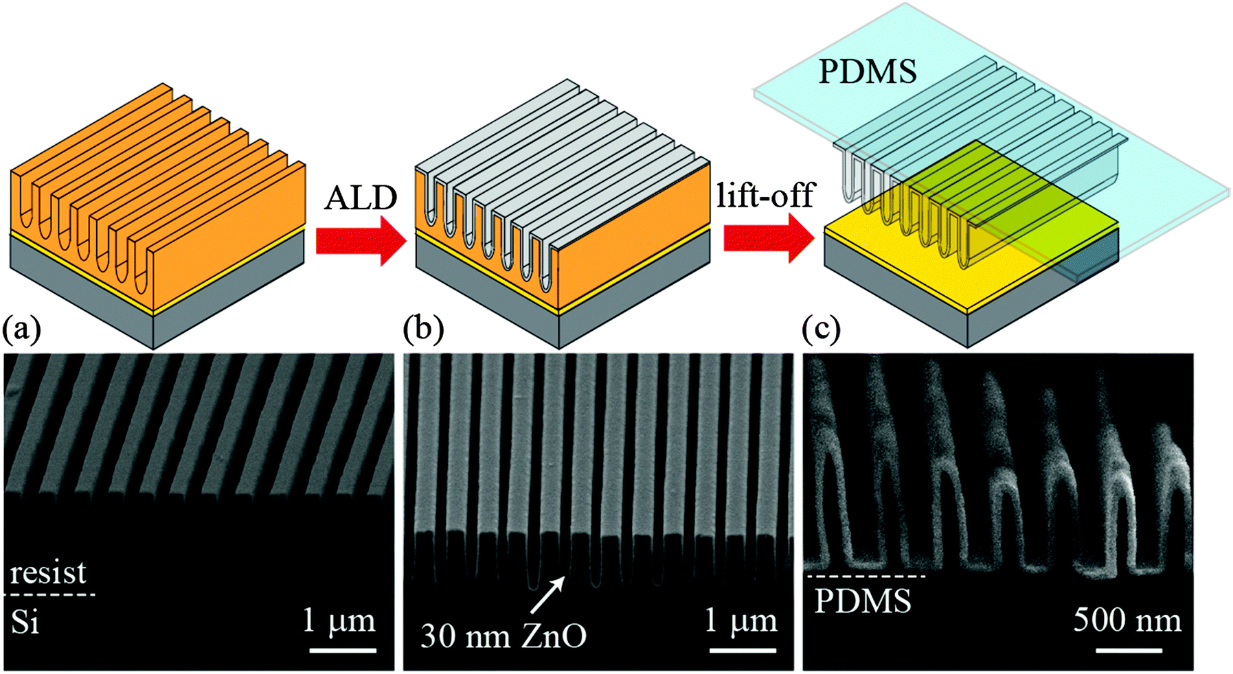 | ||
| Fig. 1 The fabrication process of multifunctional nano-accordion structures. (a) The photoresist template is patterned with 500 nm period using interference lithography. (b) A ZnO thin film is then deposited on the photoresist template using ALD. (c) The ZnO nano-accordion structure is then transferred by lift-off onto PDMS substrate by dissolving photoresist template. | ||
The proposed process can be used to fabricate ZnO/AZO nano-accordion structures over large areas with high fidelity. The structure area is limited by the lithography pattern area, which is scalable with system hardware.51 In our experiments samples with area around 20 × 20 mm2 were fabricated with few defects. Top-view SEM images of defect-free ZnO structures with 30 nm thickness and 500 nm period on PDMS is shown in Fig. 2a. Slight roughness can be observed along the top of the structure, which is the result of photoresist underexposure. Fabricated nano-accordion ZnO structures after being detached from the PDMS in various arrangements are illustrated in Fig. 2b–f.
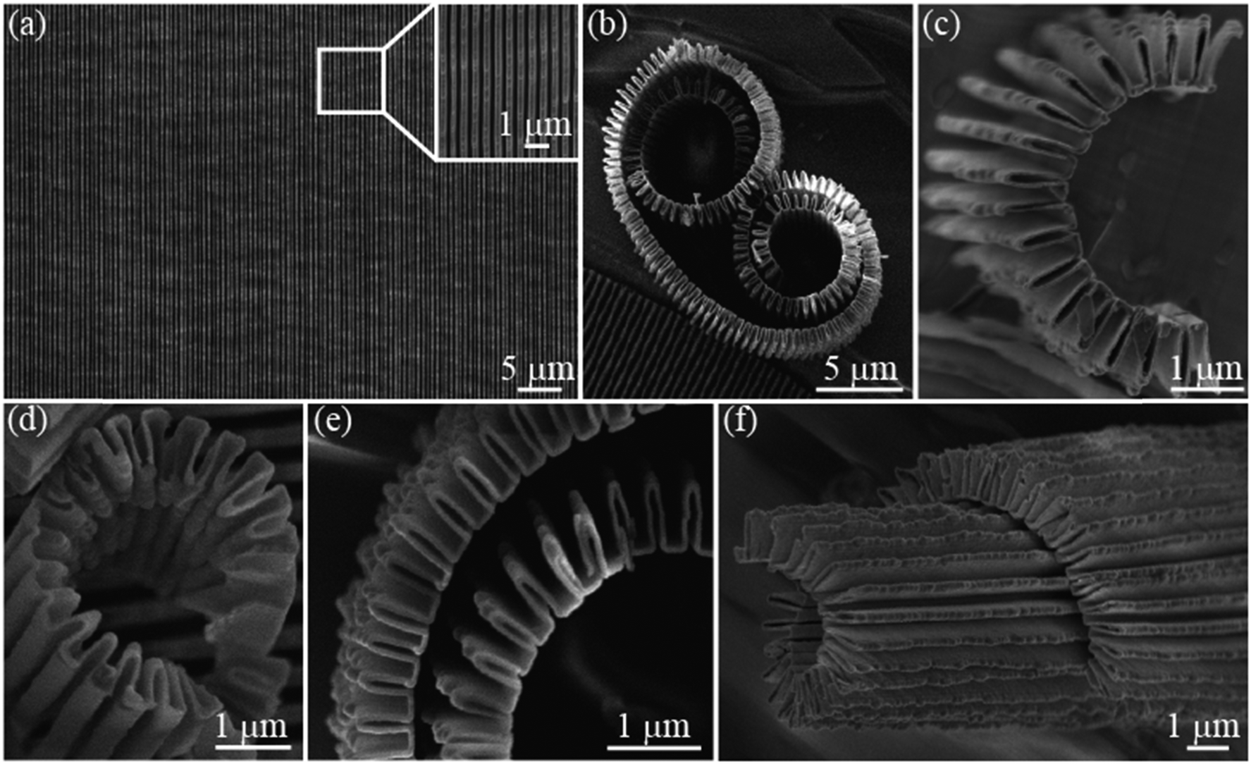 | ||
| Fig. 2 Fabricated nano-accordion structures. (a) SEM displays the large-area nano-accordion structure, composed of 30 nm thick ZnO on PDMS. The inset shows a close-up view. (b–f), SEM image of the curled ZnO nano-accordion structure in different geometrical arrangements when detached from the PDMS substrate. | ||
The stretching mechanism of nano-accordion structures is illustrated in Fig. 3, where the structures extend in the fold direction. Stretching of brittle film is facilitated by deflection and bending of individual nano-accordion elements with minimal local strain (see Supporting information A, ESI†). A nano-accordion structure with a 500 nm period, 1100 nm height, and 30 nm ZnO thickness was analyzed using uniaxial tensile tests on a mechanical stage within the SEM chamber. As the applied load is gradually increased, the corresponding material strain can be characterized by the changes in structure period as measured using SEM. The resulting SEM images at various stages of strain are illustrated in Fig. 3. The white dotted arrow serves as a ten-period marker, and increases with strain to indicate the sample stretching. Starting at 500 nm at 0% strain, the period of the nano-accordion structure gradually increased to a maximum of 755 nm at 51% strain. This strain is two orders of magnitude higher than a planar ZnO film,25 which cracks readily (see Supporting information A, ESI†). When the strain is further increased, cracks form along the fold ridge and can be systematically observed throughout the sample. Fig. 4a shows a top-view SEM of this sample at failure strain (εmax), 53%, with cracks developed on and propagated along the ridge direction. It is also important to note that since the present study on nano-accordion geometry is 1D, structure compression along the ridge direction occurs and leads to structure collapse due to buckling (see Supporting information B, ESI†). This effect can be remedied by designing a 2D accordion geometry, and is the subject of future studies.
 | ||
| Fig. 3 Stretching mechanism for the nano-accordion structure. SEM images show the 30 nm thick ZnO nano-accordion structure being stretched under tensile loading. The 10 period marker is defined by the white arrows, indicating period increase with increasing strain. No systematic failure can be observed up to 51% strain. | ||
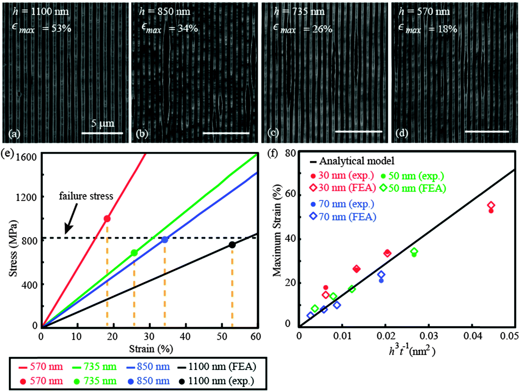 | ||
| Fig. 4 Mechanical characterization of nano-accordion structure. (a–d), Top-view SEM images showing systematic failure of nano-accordion structure along the fold ridges. The fabricated structures consist of a 30 nm thick ZnO film with (a) h = 1100 nm, εmax = 53%; (b) h = 850 nm, εmax = 34%; (c) h = 735 nm, εmax = 26%; (d) h = 570 nm, εmax = 18%. (e) Simulated maximum stress versus strain curve for a 30 nm thick ZnO nano-accordion structure with different heights. The failure strains obtained experimentally are plotted to determine corresponding local failure stress, which has an average value of 800 MPa. (f) Comparison of stretchability versus normalized geometric parameter h3/t using the analytical model, FEA, and experimental data. | ||
To understand the effect of nano-accordion height on failure strain, tensile experiments were carried out using structures with varying heights (h). The failure strains for 500 nm-period, 30 nm-thick structures with heights of 850 nm, 735 nm, and 570 nm were found to be 34%, 26%, and 18%, respectively, as depicted in Fig. 4b–d. This result indicates the stretchability of the nano-accordion structure can be improved with increased height. It is interesting to note that the failure modes for these samples are identical, where the cracks initiate and propagate along the fold ridge. Mechanical tests were also performed for structures with variable thicknesses (t), and demonstrate improved stretchability with decreasing thicknesses (see Supporting information C, ESI†). The same failure mode is observed for all samples.
Through these experiments, failure strain values for different nano-accordion geometries were obtained. However, the corresponding local stress at the fold cannot be measured directly. This information can be extracted numerically through finite element analysis (FEA) modelling of nano-accordion structure, which confirms the existence of stress concentration under tensile loading occurs within the inner curve of the nano-accordion fold structure (see Supporting information C, ESI†). The concentration of stress in this region is the result of section bending, which results in peak tensile stress at the inner section and leads to crack formation along the fold ridge. The maximum stress at the fold was numerically calculated and plotted vs. strain for 30 nm ZnO film with different nano-accordion heights in Fig. 4e. The experimentally measured failure strain values for these samples were overlaid to obtain the corresponding local stress at failure, which is denoted by the black dotted line and has an average value of 800 MPa. This is similar to reported values of planar ZnO films in literature.25 The modeling results also indicate that the maximum contribution to stretching originates from the deflection of vertical sections in the nano-accordion geometry, validating the experimental observation that taller structures have better stretchability.
To predict structure stretchability, a first-order analytical model was developed by considering a single period of nano-accordion geometry in three different components (see Supporting information A, ESI†). Individual stress–strain behaviors of these components were analyzed to obtain the total stress–strain behavior of the nano-accordion structure. The maximum stretchability, as defined by the failure strain, is given by:
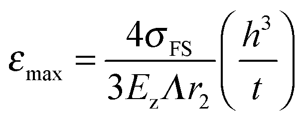 | (1) |
To further enhance the functionality of the nano-accordion structure, the ZnO film was doped with Al during the ALD process. The measured resistance for a structure with 50 nm thickness and 1100 nm height was 730 kΩ, with an effective resistivity of 0.75 Ω cm when estimating the total structure length. Note the film resistivity depends on film thickness, which can be precisely controlled during ALD. For more detailed electrical characterization of the ALD film see Supporting information D, ESI†. The structure resistance is normalized by the resistance of the unstrained sample (R/R0), and is plotted versus applied strain in Fig. 5a. The resistance increases by only 8% for strain values up to 10%. At higher strain the relative resistance increased gradually and ultimately 100 times greater at 32.5% strain. This characterization was consistent with the previous mechanical analysis that 50 nm thick structures of this height undergo systematic failure at 33% strain. Gradual resistance increase below 30% strain can be attributed to compression induced buckling of the nano-accordion structure along the fold ridge (see Supporting information B, ESI†), which can be mitigated by using a 2D fold geometry. The inset images show AZO nano-accordion structures remain conductive in a closed circuit to light an LED while being stretched from 0% to 30% (for video of experiment see ESI† Videos A and B). Constant voltage was applied, and the increased resistance at high strain can be observed as a slight decrease in light intensity.
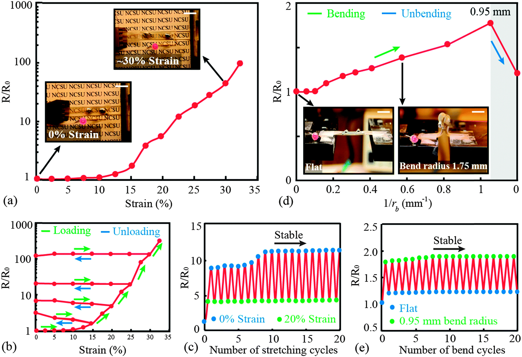 | ||
| Fig. 5 Electrical characterization of 50 nm AZO nano-accordion structures. (a) Relative resistance versus strain in static loading. Inset optical images show the AZO nano-accordion sample as a stretchable transparent conductor at 0% and ∼30% strain. Scale bars, 1 cm. (b) Relative resistance versus strain with intermediate load–unload cycles and (c) cyclic loading–unloading performance. (d) Relative resistance versus bending radius. Optical images show electrical performance for bending. Scale bars, 1 cm. (e) Relative resistance for cyclic bending and unbending performance. | ||
The electrical performance under intermediate loading was also examined, as shown in Fig. 5b. Each load–unload cycle stretches to a predetermined strain and then releases back to 0% strain, as denoted by the green and blue arrows, respectively. The cycle was repeated incrementally at strains of 15%, 20%, 25%, and 30%. When the sample was stretched to 15% strain in the first cycle, the relative resistance increased to 1.64 times due to compression induced structure breaking in the ridge direction. At this point, the broken parts of AZO film are still in contact with adjacent nano-accordion stripes and contribute to conductivity. After unloading the stripes were no longer in contact, which counterintuitively increases the relative resistance to 3.21. When the sample was stretched again, the relative resistance retraced itself to 15% strain before increasing to 5.07 at 20% strain. This increase is the result of nano-accordion stripes coming closer and re-establishing contact, thereby reducing the resistance. Increasing the strain further resulted in similar behavior until 25% strain, where dramatic resistance increases indicate further damage to the nano-accordion structure. Unlike the previous two cycles, unloading to 0% strain resulted in constant resistance, indicating that conductivity was maintained solely through the fold direction of the structures. Similar loading–unloading behavior was observed for load–unload cycles up to 32.5% strain.
Cyclic loading of 50 nm AZO nano-accordion samples was conducted to examine the repeatability of the electrical performance, where the samples were stretched to 20% strain for 20 cycles. The samples show repeatable electrical performance, as shown in Fig. 5c. The resistance increases during loading and decreases during unloading with the same mechanism as described in the previous section. The resistance stabilizes after the first few cycles, and remains constant up to 20 cycles. This indicates that the initial loading induced permanent damage attributed to structure buckling in the ridge direction. However, after the initial release, unloading and loading of the structure are driven only by elastic stretching, which results in stable and repeatable electrical performance. This repeatable strain-dependent electrical performance can be further improved through structure optimization and utilized for strain sensors that are simultaneously transparent.
The effects of bending on the electrical performance of the AZO nano-accordion structures were also investigated. Fig. 5d shows the relative resistance as a function of 1/rb, where rb is the sample bending radius. No change in resistance was observed for bend radii greater than 10 mm, beyond which the relative resistance increases almost linearly to reach 1.77 times at a bend radius of 0.95 mm. The relative resistance recovered to 1.19 times of initial resistance when unbent, indicating that the bending is dominated by structure stretching. Cyclic characterization of bending–unbending to a radius of 0.95 mm is plotted in Fig. 5e. No significant increase in resistance was observed up to 20 cycles, indicating high repeatability of electrical properties under bending. In these experiments the structures were on the outer surface of the bent PDMS substrate, but similar properties can be observed with the structure on the inner bent surface (see Supporting information D, ESI†). Inset images show the AZO nano-accordion structure remains conductive to light an LED as the sample is bent to a radius of 1.75 mm (for video of experiment see ESI† Videos C and D). These results show that the nano-accordion AZO conductors are suitable for applications involving uniaxial stretching and for cylindrical surfaces.
In addition to being stretchable, bendable, and conductive, the nano-accordion structures are also transparent due to their thin thicknesses. The total broadband optical transmittance spectra of 30 nm, 50 nm, and 70 nm thick AZO nano-accordion structures are shown in Fig. 6a. Here the structures have a constant period of 500 nm and height of 1100 nm. Theoretical transmittances calculated using finite-difference time-domain (FDTD) are overlaid (see Supporting information E, ESI†). The transmission dips in the near-infrared range are attributed to the intrinsic property of the PDMS substrate, which is not modelled in the FDTD simulation. It was observed that the transmittance was inversely related to the AZO film thickness, with the transmission at 633 nm wavelength decreasing from 79.7% to 74.2% to 69.1% for thicknesses of 30, 50, and 70 nm, respectively. Lower transmittance in the short wavelength region may have resulted from scattering loss due to line-edge roughness along fold geometry, absorption, as well as diffraction loss due to diffraction within the PDMS substrate (see Supporting information F, ESI†). These effects can be removed by further reducing the period of the nano-accordion geometry to less than 200 nm, which is half of the operating wavelength range in the visible spectrum. More discussion on the anisotropic optical properties and scattering losses is included in Supporting information F, ESI†.
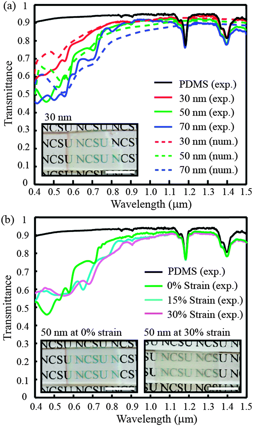 | ||
| Fig. 6 Optical characterization of AZO nano-accordion structures. (a) Experimental and numerical simulation for transmittance spectra of 30 nm, 50 nm, and 70 nm thick AZO nano-accordion structures. An optical image of the 30 nm structure is shown in the inset. Scale bar, 1 cm. (b) Transmittance spectra of 50 nm AZO nano-accordion structure under 0%, 15%, and 30% strain. Optical images of the 50 nm structure at 0% and 30% strain are shown in the inset. Scale bars, 1 cm. | ||
The effect of strain on optical transmittance of 50 nm AZO nano-accordion structures is illustrated in Fig. 6b, where the sample was stretched to 15% and 30% strains. It was observed that transmittance from 600 to 1000 nm decreased slightly with strain. This can be attributed to diffraction effects, since the structure period is larger while strained. It is interesting to note that the average transmittance between 400 and 600 nm wavelength increased from 50% to 60% under both strains, indicating that optical losses have been reduced. These results indicate that stretching of the structure does not monotonically decrease optical transmission over broadband, which depends on the geometry of the optical nanostructure. More efficient geometries could be created through rigorous design to optimize the optical effects, and is the subject of future studies.
The demonstrated physical properties of the structure can be further improved by optimizing the nano-accordion geometry. Optical transmittance in the visible wavelength range can be increased by decreasing the structure thickness. Decreasing the nano-accordion thickness would also simultaneously improve mechanical stretchability. However, it may also lead to an increase in resistance and degrade electrical performance. To eliminate diffraction losses in the visible range, the nano-accordion period can be further decreased to subwavelength values. This also has the added benefit of further enhancing mechanical stretchability by increasing fold density. The structure line-edge roughness is also a potential source of scattering loss, and can be mitigated through better control during lithography or through an annealing process. The roughness may also be a source of crack initiation when strain is applied, and if reduced may improve mechanical properties. Loss of electrical conductivity due to compression induced breaking of the nano-accordion film under stretching can be eliminated by designing a 2D nano-accordion geometry and is currently being explored. 2D nano-accordion geometry will enable biaxial stretchability and will make it suitable for applications involving spherical surfaces.39
Conclusions
In summary, we have developed a nanostructured material with a unique combination of electrical conductivity, mechanical stretchability, and optical transparency. Using interference lithography and ALD, this fabrication process allows precise control over the nano-accordion structure geometries and material composition to tailor material properties in multiple physical domains. The stretchability of 30 nm thick ZnO and aluminum doped zinc oxide (AZO) films have been dramatically increased to 51%, which is two orders of magnitude better than planar films. This stretchability is profoundly dominated by the structure geometry, and shows dramatic improvements as the structures are made taller and thinner. Numerical and analytical models developed to describe mechanical behavior exhibit agreement with experimental data and can be used to predict the optimal scaling parameters. The nano-accordion structures also have repeatable electrical performance over 20 cycles of stretching and bending, and exhibit up to 70% optical transmission over the visible spectrum. The proposed nano-accordion structures can be incorporated into functional devices either as connectors for in-plane elements6 or stacked out-of-plane using transfer printing techniques.4 The capability to engineer these nano-accordion structures can potentially lead to novel electronics and sensors that are simultaneously transparent, stretchable, and wearable.Experimental section
Fabrication and transfer of nano-accordion structure
Silicon wafers were spincoated with 98 nm of antireflection coating (ARC i-CON-16, Brewer Science, Inc.) to reduce back reflection during lithography, and a positive-tone photoresist (Sumitomo PFi88A7). A HeCd laser with 325 nm wavelength was used for interference lithography to make a photoresist template. The nano-accordion structure height is controlled by the resist thickness and exposure dose during this step. The nano-accordion structure height was controlled by varying the exposure dose. The structure height can also be controlled by photoresist thickness, but it was kept constant at 1.5 μm for all the samples used. The structure period was kept constant at 500 nm, but could be specified to a broad range as desired.Photoresist nanostructure templates were subsequently coated with ZnO (or Al-doped ZnO) using atomic layer deposition (ALD) in a custom made viscous-flow, hot-walled, vacuum reactor described previously.52,53 The reactor was kept around 550 mTorr at 90 °C. In a typical ALD cycle, a metal-containing precursor is first dosed into the chamber, followed with high purity nitrogen purge (Machine & Welding Supply Co, further purified with an Entegris GateKeeper). Subsequently, a co-reactant (deionized water) is dosed into the reactor, followed with another nitrogen purge. Diethyl zinc (DEZ, Strem Chemicals, min 98% pure) was used as the metal-containing precursor for ZnO, and trimethylaluminum (TMA, Strem Chemicals, min 98% pure) for doping ZnO thin films. ZnO thin films were deposited using DEZ–water ALD cycles, and the growth rate is ∼1.6 Å per cycle. Aluminum-doped zinc oxide (AZO) thin films were deposited in a prescribed number of laminates, consisting of 13 DEZ–water cycles followed by 1 TMA–water cycle, to achieve the desired film thickness. Growth per laminate was roughly 23.8 Å. AZO films are deposited with 13![[thin space (1/6-em)]](https://www.rsc.org/images/entities/char_2009.gif) :1 ratio for ZnO and Al2O3 to ensure similar mechanical properties to ZnO. In both cases silicon substrates (University Wafers, P-type, 〈100〉) were placed in the front and back of the reactor chamber and used as monitors for film growth. Film thickness was determined using an α-SE ellipsometer (J.A. Woollam Co., Inc.).
:1 ratio for ZnO and Al2O3 to ensure similar mechanical properties to ZnO. In both cases silicon substrates (University Wafers, P-type, 〈100〉) were placed in the front and back of the reactor chamber and used as monitors for film growth. Film thickness was determined using an α-SE ellipsometer (J.A. Woollam Co., Inc.).
ALD coated samples and PDMS substrates were then each treated with O2 plasma to remove organic contaminants and promote adhesion. The PDMS substrate was then bonded with the ALD coated samples and immersed in n-methyl-2-pyrrolidone (NMP) for 48 hours to dissolve the photoresist template. The photoresist was underexposed during lithography to facilitate structure transfer during the lift-off process. Upon photoresist removal, the nano-accordion ZnO/AZO structure was separated from silicon and transferred to PDMS. The sample was heated in a furnace (Vulcan 3 series) at 65 °C for approximately 5 hours to outgas NMP absorbed in the PDMS.
Mechanical simulation
A 2D calculation of the stress distribution in the nano-accordion structure was carried out using commercially available FEA software (ANSYS 14.5). A 2D model with plane strain conditions was assumed due to the larger dimension along the ridge direction. Additionally, due to the large thickness of the PDMS substrate compared to the ZnO nano-accordion geometry, deformation of PDMS was constrained in the direction normal to stretching. A quadrilateral 8-node diffusion element, PLANE238 was used to model both the PDMS and ZnO structure. The 2D elements share nodes at the PDMS–ZnO contact region.Optical measurement and simulation
Optical measurements were carried out using a UV-Vis-NIR spectrophotometer (Agilent Cary 5000). Optical simulations were conducted using Lumerical's FDTD Solutions 8.9. One cell of the periodic nanostructures was constructed in 2D with periodic boundary conditions along the x direction and absorbing boundary conditions along the y direction (see Supporting information E, ESI†). The structures were directly illuminated by a pulsed light source for spectral analysis. PDMS was assumed to be non-dispersive with a refractive index of 1.44 and the nanostructure material was set to ZnO with Sellmeir dispersion obtained by ellipsometric measurements of a ZnO film deposited by ALD. For both experimental and numerical measurements, unpolarized transmission spectra were calculated by averaging TE and TM results.Acknowledgements
We gratefully acknowledge the students, staff, and facility support from the North Carolina State University Nanofabrication Facility (NNF) and Analytical Instrumentation Facility (AIF). This work was supported by a NASA Office of the Chief Technologist's Space Technology Research Opportunity – Early Career Faculty grant (grant NNX12AQ46G).References
- G. H. Gelinck, H. E. A. Huitema, E. van Veenendaal, E. Cantatore, L. Schrijnemakers, J. B. P. H. van der Putten, T. C. T. Geuns, M. Beenhakkers, J. B. Giesbers, B.-H. Huisman, E. J. Meijer, E. M. Benito, F. J. Touwslager, A. W. Marsman, B. J. E. van Rens and D. M. de Leeuw, Nat. Mater., 2004, 3, 106–110 CrossRef CAS PubMed.
- J. A. Rogers, Z. Bao, K. Baldwin, A. Dodabalapur, B. Crone, V. R. Raju, V. Kuck, H. Katz, K. Amundson, J. Ewing and P. Drzaic, Proc. Natl. Acad. Sci. U. S. A., 2001, 98, 4835–4840 CrossRef CAS PubMed.
- T. Sekitani, H. Nakajima, H. Maeda, T. Fukushima, T. Aida, K. Hata and T. Someya, Nat. Mater., 2009, 8, 494–499 CrossRef CAS PubMed.
- R.-H. Kim, M.-H. Bae, D. G. Kim, H. Cheng, B. H. Kim, D.-H. Kim, M. Li, J. Wu, F. Du, H.-S. Kim, S. Kim, D. Estrada, S. W. Hong, Y. Huang, E. Pop and J. A. Rogers, Nano Lett., 2011, 11, 3881–3886 CrossRef CAS PubMed.
- D. J. Lipomi, B. C.-K. Tee, M. Vosgueritchian and Z. Bao, Adv. Mater., 2011, 23, 1771–1775 CrossRef CAS PubMed.
- D.-H. Kim, N. Lu, R. Ma, Y.-S. Kim, R.-H. Kim, S. Wang, J. Wu, S. M. Won, H. Tao, A. Islam, K. J. Yu, T. Kim, R. Chowdhury, M. Ying, L. Xu, M. Li, H.-J. Chung, H. Keum, M. McCormick, P. Liu, Y.-W. Zhang, F. G. Omenetto, Y. Huang, T. Coleman and J. A. Rogers, Science, 2011, 333, 838–843 CrossRef CAS PubMed.
- W.-H. Yeo, Y.-S. Kim, J. Lee, A. Ameen, L. Shi, M. Li, S. Wang, R. Ma, S. H. Jin, Z. Kang, Y. Huang and J. A. Rogers, Adv. Mater., 2013, 25, 2773–2778 CrossRef CAS PubMed.
- S. Yao and Y. Zhu, Nanoscale, 2014, 6, 2345–2352 RSC.
- T. Someya, T. Sekitani, S. Iba, Y. Kato, H. Kawaguchi and T. Sakurai, Proc. Natl. Acad. Sci. U. S. A., 2004, 101, 9966–9970 CrossRef CAS PubMed.
- B. C.-K. Tee, C. Wang, R. Allen and Z. Bao, Nat. Nanotechnol., 2012, 7, 825–832 CrossRef CAS PubMed.
- G. Schwartz, B. C.-K. Tee, J. Mei, A. L. Appleton, D. H. Kim, H. Wang and Z. Bao, Nat. Commun., 2013, 4, 1859 CrossRef PubMed.
- M. L. Hammock, A. Chortos, B. C.-K. Tee, J. B.-H. Tok and Z. Bao, Adv. Mater., 2013, 25, 5997–6038 CrossRef CAS PubMed.
- C. Wang, D. Hwang, Z. Yu, K. Takei, J. Park, T. Chen, B. Ma and A. Javey, Nat. Mater., 2013, 12, 899–904 CrossRef CAS PubMed.
- M. Zirkl, A. Haase, A. Fian, H. Schön, C. Sommer, G. Jakopic, G. Leising, B. Stadlober, I. Graz, N. Gaar, R. Schwödiauer, S. Bauer-Gogonea and S. Bauer, Adv. Mater., 2007, 19, 2241–2245 CrossRef CAS PubMed.
- T. Yamada, Y. Hayamizu, Y. Yamamoto, Y. Yomogida, A. Izadi-Najafabadi, D. N. Futaba and K. Hata, Nat. Nanotechnol., 2011, 6, 296–301 CrossRef CAS PubMed.
- D. J. Lipomi, M. Vosgueritchian, B. C.-K. Tee, S. L. Hellstrom, J. A. Lee, C. H. Fox and Z. Bao, Nat. Nanotechnol., 2011, 6, 788–792 CrossRef CAS PubMed.
- J. Lee, P. Lee, H. Lee, D. Lee, S. S. Lee and S. H. Ko, Nanoscale, 2012, 4, 6408–6414 RSC.
- C. Pang, G.-Y. Lee, T. Kim, S. M. Kim, H. N. Kim, S.-H. Ahn and K.-Y. Suh, Nat. Mater., 2012, 11, 795–801 CrossRef CAS PubMed.
- K.-Y. Shin, J.-Y. Hong and J. Jang, Chem. Commun., 2011, 47, 8527–8529 RSC.
- P. Gutruf, C. M. Shah, S. Walia, H. Nili, A. S. Zoolfakar, C. Karnutsch, K. Kalantar-zadeh, S. Sriram and M. Bhaskaran, NPG Asia Mater., 2013, 5, e62 CrossRef CAS PubMed.
- K. Nomura, H. Ohta, A. Takagi, T. Kamiya, M. Hirano and H. Hosono, Nature, 2004, 432, 488–492 CrossRef CAS PubMed.
- C. G. Granqvist and A. Hultåker, Thin Solid Films, 2002, 411, 1–5 CrossRef CAS.
- F. Maldonado and A. Stashans, J. Phys. Chem. Solids, 2010, 71, 784–787 CrossRef CAS PubMed.
- N. P. Dasgupta, S. Neubert, W. Lee, O. Trejo, J.-R. Lee and F. B. Prinz, Chem. Mater., 2010, 22, 4769–4775 CrossRef CAS.
- C. W. Ong, D. G. Zong, M. Aravind, C. L. Choy and D. R. Lu, J. Mater. Res., 2003, 18, 2464–2472 CrossRef CAS.
- A. Russo, B. Y. Ahn, J. J. Adams, E. B. Duoss, J. T. Bernhard and J. A. Lewis, Adv. Mater., 2011, 23, 3426–3430 CrossRef CAS PubMed.
- B. Y. Ahn, D. J. Lorang and J. A. Lewis, Nanoscale, 2011, 3, 2700–2702 RSC.
- D. C. Hyun, M. Park, C. Park, B. Kim, Y. Xia, J. H. Hur, J. M. Kim, J. J. Park and U. Jeong, Adv. Mater., 2011, 23, 2946–2950 CrossRef CAS PubMed.
- K.-Y. Chun, Y. Oh, J. Rho, J.-H. Ahn, Y.-J. Kim, H. R. Choi and S. Baik, Nat. Nanotechnol., 2010, 5, 853–857 CrossRef CAS PubMed.
- X. Li, Y. Zhu, W. Cai, M. Borysiak, B. Han, D. Chen, R. D. Piner, L. Colombo and R. S. Ruoff, Nano Lett., 2009, 9, 4359–4363 CrossRef CAS PubMed.
- K. S. Kim, Y. Zhao, H. Jang, S. Y. Lee, J. M. Kim, K. S. Kim, J.-H. Ahn, P. Kim, J.-Y. Choi and B. H. Hong, Nature, 2009, 457, 706–710 CrossRef CAS PubMed.
- Z. Chen, W. Ren, L. Gao, B. Liu, S. Pei and H.-M. Cheng, Nat. Mater., 2011, 10, 424–428 CrossRef CAS PubMed.
- F. Xu and Y. Zhu, Adv. Mater., 2012, 24, 5117–5122 CrossRef CAS PubMed.
- S. Yun, X. Niu, Z. Yu, W. Hu, P. Brochu and Q. Pei, Adv. Mater., 2012, 24, 1321–1327 CrossRef CAS PubMed.
- K. H. Kim, M. Vural and M. F. Islam, Adv. Mater., 2011, 23, 2865–2869 CrossRef CAS PubMed.
- T. Sekitani, Y. Noguchi, K. Hata, T. Fukushima, T. Aida and T. Someya, Science, 2008, 321, 1468–1472 CrossRef CAS PubMed.
- L. Hu, M. Pasta, F. L. Mantia, L. Cui, S. Jeong, H. D. Deshazer, J. W. Choi, S. M. Han and Y. Cui, Nano Lett., 2010, 10, 708–714 CrossRef CAS PubMed.
- D.-H. Kim, J.-H. Ahn, W. M. Choi, H.-S. Kim, T.-H. Kim, J. Song, Y. Y. Huang, Z. Liu, C. Lu and J. A. Rogers, Science, 2008, 320, 507–511 CrossRef CAS PubMed.
- H. C. Ko, M. P. Stoykovich, J. Song, V. Malyarchuk, W. M. Choi, C.-J. Yu, J. B. Geddes Iii, J. Xiao, S. Wang, Y. Huang and J. A. Rogers, Nature, 2008, 454, 748–753 CrossRef CAS PubMed.
- J. A. Rogers, T. Someya and Y. Huang, Science, 2010, 327, 1603–1607 CrossRef CAS PubMed.
- D.-Y. Khang, H. Jiang, Y. Huang and J. A. Rogers, Science, 2006, 311, 208–212 CrossRef CAS PubMed.
- W. M. Choi, J. Song, D.-Y. Khang, H. Jiang, Y. Y. Huang and J. A. Rogers, Nano Lett., 2007, 7, 1655–1663 CrossRef CAS PubMed.
- F. Xu, X. Wang, Y. Zhu and Y. Zhu, Adv. Funct. Mater., 2012, 22, 1279–1283 CrossRef CAS PubMed.
- S. Yao and Y. Zhu, Adv. Mater., 2015, 27, 1480–1511 CrossRef CAS PubMed.
- C. F. Guo, T. Sun, Q. Liu, Z. Suo and Z. Ren, Nat. Commun., 2014, 5, 3121 Search PubMed.
- G. N. Greaves, A. L. Greer, R. S. Lakes and T. Rouxel, Nat. Mater., 2011, 10, 823–837 CrossRef CAS PubMed.
- X. Zheng, H. Lee, T. H. Weisgraber, M. Shusteff, J. DeOtte, E. B. Duoss, J. D. Kuntz, M. M. Biener, Q. Ge, J. A. Jackson, S. O. Kucheyev, N. X. Fang and C. M. Spadaccini, Science, 2014, 344, 1373–1377 CrossRef CAS PubMed.
- L. R. Meza, S. Das and J. R. Greer, Science, 2014, 345, 1322–1326 CrossRef CAS PubMed.
- H. I. Smith, Phys. E, 2001, 11, 104–109 CrossRef.
- A. Bagal and C.-H. Chang, Opt. Lett., 2013, 38, 2531–2534 CrossRef PubMed.
- R. K. Heilmann, C. G. Chen, P. T. Konkola and M. L. Schattenburg, Nanotechnology, 2004, 15, S504 CrossRef.
- J. C. Spagnola, B. Gong, S. A. Arvidson, J. S. Jur, S. A. Khan and G. N. Parsons, J. Mater. Chem., 2010, 20, 4213–4222 RSC.
- B. Gong, Q. Peng, J. S. Jur, C. K. Devine, K. Lee and G. N. Parsons, Chem. Mater., 2011, 23, 3476–3485 CrossRef CAS.
Footnote |
| † Electronic supplementary information (ESI) available. See DOI: 10.1039/c5mh00070j |
| This journal is © The Royal Society of Chemistry 2015 |