
 Open Access Article
 This Open Access Article is licensed under a
 Creative Commons Attribution 3.0 Unported Licence
Non-aqueous electrodeposition of functional semiconducting metal chalcogenides: Ge2Sb2Te5 phase change memory†
Philip N.
Bartlett
a,
Sophie L.
Benjamin
a,
C. H.
(Kees) de Groot
b,
Andrew L.
Hector
a,
Ruomeng
Huang
b,
Andrew
Jolleys
a,
Gabriela P.
Kissling
a,
William
Levason
a,
Stuart J.
Pearce
b,
Gillian
Reid
*a and
Yudong
Wang
b
aChemistry, University of Southampton, Southampton, SO17 1BJ, UK. E-mail: G.Reid@soton.ac.uk
bElectronics and Computer Science, University of Southampton, Southampton, SO17 1BJ, UK
First published on 1st April 2015
Abstract
We report a new method for electrodeposition of device-quality metal chalcogenide semiconductor thin films and nanostructures from a single, highly tuneable, non-aqueous electrolyte. This method opens up the prospect of electrochemical preparation of a wide range of functional semiconducting metal chalcogenide alloys that have applications in various nano-technology areas, ranging from the electronics industry to thermoelectric devices and photovoltaic materials. The functional operation of the new method is demonstrated by means of its application to deposit the technologically important ternary Ge/Sb/Te alloy, GST-225, for fabrication of nanostructured phase change memory (PCM) devices and the quality of the material is confirmed by phase cycling via electrical pulsed switching of both the nano-cells and thin films.
Conceptual insightsSemiconducting metal chalcogenides are of increasing importance for emerging micro- and nano-electronic applications in renewable energy, solid state memory and 3D metamaterials. However, the demand for smaller, higher performance, more energy-efficient electronics, is pushing conventional materials deposition and device fabrication methods to their intrinsic limits. ‘Top-down’ vapour deposition methods are not suitable for filling high aspect-ratio vias in structures that may be the basis of future devices. Electrodeposition offers several potentially significant advantages: it is a faster and much lower cost alternative to vapour deposition, and as a ‘bottom-up’ growth method, it can fill 2D and 3D nanostructures selectively. Electrodeposition is therefore an extremely attractive prospect for the production of nano-structured materials and devices. To demonstrate the enormous potential of electrodeposition for metal chalcogenide growth, we selected the ternary alloy, GST-225 (Ge2Sb2Te5) – one of the most challenging chalcogenide materials, and widely regarded to be the most promising candidate to scale non-volatile memory beyond the Flash memory architecture. We describe here the deposition of functional GST-225 from a single, non-aqueous electrolyte (containing custom-made reagents for the three elements), demonstrating fine compositional control, creation of high density nanocells (<100 nm), extremely well-controlled electrical functionality, and repeated cycling between the amorphous and crystalline phases. |
1. Introduction
Semiconducting metal chalcogenides represent an exciting class of tuneable band gap materials which are increasingly demonstrating potential in a diversity of micro- and nano-electronic applications, particularly related to renewable energy,1–3 solid state memory4 and in complex 3D metamaterials.5 In this paper we show that non-aqueous electrodeposition is capable of device-quality deposition, comparable with state-of-the-art, with the additional advantages inherent to electrodeposition, such as high aspect ratio filling, 3D deposition, and highly efficient material use.Common methods to deposit metal chalcogenides for device applications use physical vapour deposition (PVD), chemical vapour deposition (CVD) or atomic layer deposition (ALD).6–10 These allow growth of ternary alloys of device quality. However, while these ‘top-down’ deposition methods are widely used for growing thin metallic and semiconducting films, PVD and CVD, in particular, are not suitable for filling high aspect ratio vias in structures that may be the basis of future devices, such as solid-state memory cells.9,10 ALD is effective here, however it suffers from inherently slow deposition rates.
Electrodeposition offers several potentially significant advantages for growth of semiconductor alloys. It is a faster and much lower cost alternative to the vapour deposition techniques as it does not require ultra-high vacuum (UHV) equipment or high temperatures. Importantly, as a ‘bottom-up’ growth method, it can be used to fill lithographically nanopatterned substrates and 3-dimensional nanostructures selectively.11–15 Thus electrodeposition is an extremely attractive prospect for the production of nano-structured metal chalcogenides and the creation of nanoscale devices.
Electrodeposition from both aqueous solution and ionic liquids15–17 has been used for a range of semiconductor materials, but the deposition of metal chalcogenides is not straightforward, especially when requiring both the incorporation of germanium, which is challenging by electrodeposition, as well as control over the composition and quality of binary or ternary material. To illustrate the feasibility of non-aqueous electrodeposition from an appropriately designed system to address these problems, we report the electrodeposition and characterisation of the most important functional phase change memory (PCM) material, formed of germanium, antimony and tellurium, Ge2Sb2Te5 (GST-225).
Phase change memory is one of the more challenging applications of semiconducting metal chalcogenides as it requires ternary alloys, high density cells (sub 100 nm pattern), and extremely well-controlled electrical functionality, with cycling between the amorphous and crystalline phases. PCM is a non-volatile memory type that works on the principle of probing the resistivity of the memory material, which is either amorphous or crystalline, by means of an electrical pulse. Rewriting of the memory bits is achieved by either re-crystallising an amorphous cell with a medium-amplitude voltage SET pulse or re-amorphising a crystalline cell with a high-amplitude voltage RESET pulse (cycling).6–9 Materials required for PCM applications are characterised by their high contrast between the resistances of the crystalline and amorphous phases, very fast phase transition speeds (tens of nanoseconds) and high stabilities. Chalcogenide-based PCM materials are among the most promising candidates to scale non-volatile memory beyond the Flash memory architecture,6–9 with the ternary Ge2Sb2Te5 (GST-225) the most widely used.
Electrodeposition is an extremely attractive prospect for the creation of individual memory cell devices on the scale of tens of nm in all dimensions, which, depending upon the nature of the template, can be well-insulated from one-another, therefore eliminating thermal ‘cross-talk’ between memory cells. This would contribute strongly to both reducing the power demands for switching and increasing the cycling lifetime.18,19
Some notable successes have been achieved by using a combined CVD and ALD system, leading to deposition of GST-225 into ca. 120 nm diameter pores (length = 2500 nm), although electrical cycling was not demonstrated.20,21 Stickney and co-workers have also described electrochemical ALD as an alternative, solution-based flow method for the deposition of GST22,23 by sequential electrodeposition of monolayers of each element from aqueous solutions using underpotential deposition. This method allows filling of 3D structured electrode substrates, although the layer-by-layer deposition is inherently slow.23 Electrical characterisation was performed to demonstrate basic phase change memory functionality.
2. Results and discussion
The electrodeposition of GexSbyTez alloys from a single electrolyte presents several significant challenges. The process is characterised by various degrees of freedom, caused by the distinct electrochemical properties of the individual elements, the interactions between the various precursor species present to deliver the elements, the effect of the supporting electrolyte on the solution speciation, as well as the interactions between the electrolyte species and the substrate. Moreover, functional PCM devices place significant demands on the material quality, to achieve the purity and uniformity necessary for stable phase change performance. However, if it can be achieved, electrodeposition from a single electrolyte has the added advantages of allowing fast, high-throughput characterisation of the phase diagram either via multiple experiments, or in a single experiment by applying a non-uniform voltage across the sample.We have previously developed a non-aqueous electrolyte system that allows electrodeposition of a range of individual p-block elements from tetrabutylammonium chlorometallate precursors onto planar electrodes.24,25 The benefits of using these particular precursors are their high solubility in (non-coordinating) CH2Cl2 and their accessible reduction potentials. We now demonstrate that they are also mutually compatible in solution, therefore allowing the preparation of electrolyte baths from a very wide range of precursor ratios.
In order to successfully electrodeposit the ternary GST-225 with compositional control and high quality, it is necessary to prepare a suitable chlorogermanate salt. [NnBu4][GeIICl3] was found to be incompatible with [NnBu4]2[TeCl6] in CH2Cl2 solution, causing the reduction of Te(IV) to elemental Te, with concomitant oxidation of the Ge(II). However, combining [NnBu4][GeIVCl5], [NnBu4][SbCl4] and [NnBu4]2[TeCl6], in the presence of excess [NnBu4]Cl in CH2Cl2, gave a stable electrolyte bath.
Fig. 1a shows overlaid cyclic voltammograms for the individual precursors. The labelled peaks correspond to the potentials for reduction of the chlorometallate anions to the elements. The [SbCl4]− is reduced most easily (−0.74 V), followed by the [TeCl6]2− (−1.15 V); however, the onset of the [TeCl6]2− reduction is more anodic than the [SbCl4]− reduction due to a difference in the nucleation overpotential, and tellurium can be readily deposited at potentials as positive as −0.5 V. The voltammograms for the [GeCl5]− system show two peaks. The first corresponds to the reduction of GeIV to GeII,26–30 while reduction to Ge0 only occurs at −1.52 V, significantly more cathodic than for the other elements.
 | ||
Fig. 1 (a) Cyclic voltammograms of the individual precursors and (b) the combined electrolyte recorded on glassy carbon. The grey traces show the electrochemical signal for the supporting electrolyte. For the precursor voltammetry in (a) the peak potentials of the reduction reactions are labelled with Ge (−1.52 V), Te (−1.15 V) and Sb (−0.74 V). All voltammograms were recorded with 1 × 10⁻² mol dm−3 of the precursor in 0.1 mol dm−3 [NnBu4]Cl in CH2Cl2. The combined electrolyte for the Ge2Sb2Te5 preparation in (b) contained (1![[thin space (1/6-em)]](https://www.rsc.org/images/entities/char_2009.gif) :1:2) × 10−3 mol dm−3 Ge:Sb:Te, the three observed waves are associated with the three precursors; (c) a composition triangle for varying Sb precursor concentrations and the corresponding compositions obtained for 2 μm thick films (coloured circles), the concentrations of the Ge and Te precursors were 1 mM and 2 mM, respectively. The pink star indicates the position of stoichiometric Ge2Sb2Te5. :1:2) × 10−3 mol dm−3 Ge:Sb:Te, the three observed waves are associated with the three precursors; (c) a composition triangle for varying Sb precursor concentrations and the corresponding compositions obtained for 2 μm thick films (coloured circles), the concentrations of the Ge and Te precursors were 1 mM and 2 mM, respectively. The pink star indicates the position of stoichiometric Ge2Sb2Te5. | ||
A cyclic voltammogram representative of the optimised electrolyte required for the deposition of smooth Ge2Sb2Te5 thin films is shown (Fig. 1b), using an electrolyte concentration of 1:1:2 mM [NnBu4][GeCl5]:[NnBu4][SbCl4]:[NnBu4]2[TeCl6]. The two peaks at approximately −0.44 and −0.97 V and the shoulder at −1.61 V can be associated with the reduction peaks for the individual Sb, Te and Ge reagents, respectively. In order to ensure the electrodeposition of Ge2Sb2Te5, the experiments were performed potentiostatically at −1.75 V.
The composition of the as-deposited GST can be tuned by adjusting the concentration of the chlorometallate precursors in the electrolyte. This is exemplified in Fig. 1c, which represents average energy dispersive X-ray (EDX) compositions obtained on approximately 2 μm thick films deposited at −1.75 V in electrolytes with increasing [SbCl4]− concentration. The thickness of the deposited films was controlled approximately via the charge passed (see ESI†); due to the difference in the number of electrons necessary for the reduction of the various ions, approximations were made and the elemental ratio for GST-225 was taken into account. In order to obtain the required film composition, the electrolyte formulation was re-adjusted when conditions, such as the overall electrolyte concentration or the deposition potential were changed. Importantly, the film composition was reproducible from a specific electrolyte.
A cross-sectional scanning electron microscopy (SEM) image of a GST-225 thin film deposited at −1.75 V for 110 seconds (Fig. 2a) shows that the film has uniform thickness (∼100 nm).
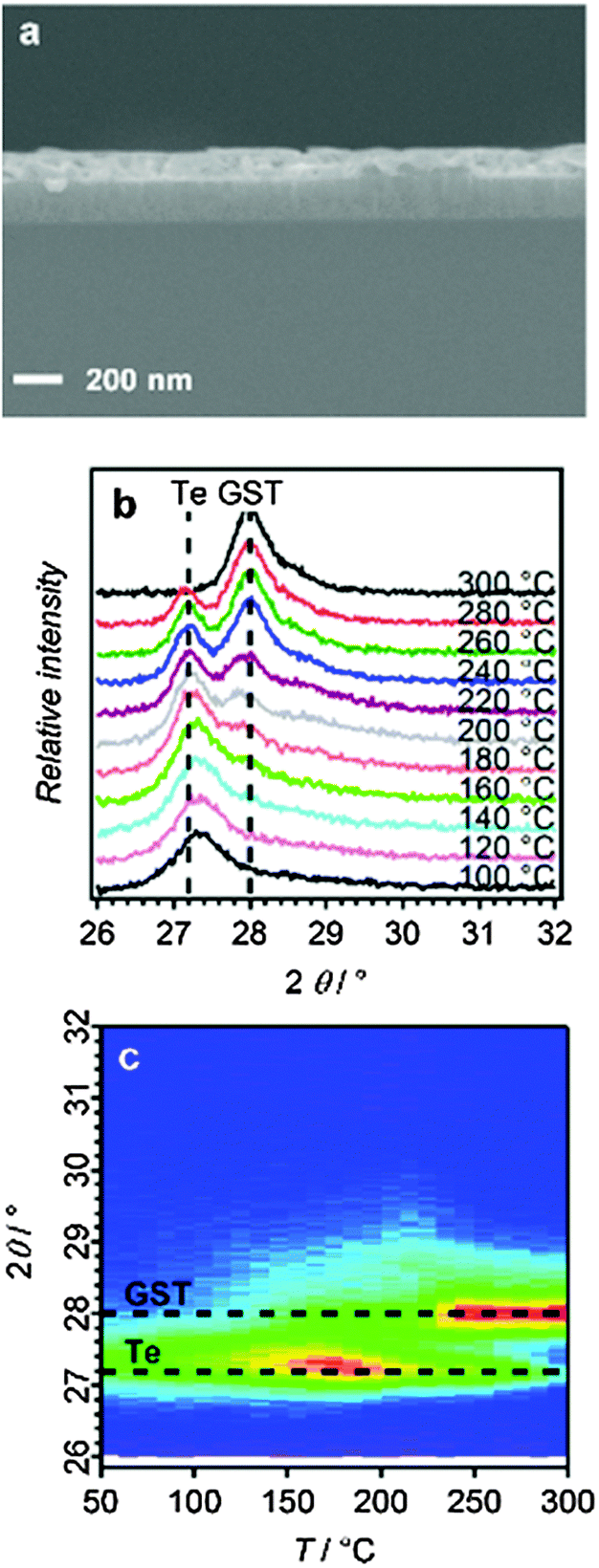 | ||
| Fig. 2 (a) Cross-section SEM image of the annealed (300 °C for 10 min) GST-225 film formed by electrodeposition. (b) XRD patterns and (c) XRD annealing map recorded as a function of temperature for GST-225 showing decreasing Te peak intensity with concomitant growth of the GST peak in this 2θ range. | ||
The crystallisation of the as-deposited ternary film was studied in situ by thin film X-ray diffraction on a hot-stage under an inert (N2) atmosphere. Fig. 2b shows a selection of XRD patterns (in the range 2θ = 26–32°) as a function of increasing temperature, together with an annealing map generated from the hot-stage XRD experiments. The initial (as-deposited) film shows only some crystalline tellurium; the germanium and antimony are presumed to be amorphous. Upon annealing, a phase change begins at around 150 °C, which is completed at around 300 °C with the disappearance of the tellurium peak and the gradual appearance of a peak corresponding to the trigonal (stable) phase of GST (2θ = 28°) (Fig. 2c).31 Repeating the annealing with prolonged periods at intermediate temperatures did not affect the XRD patterns, indicating a temperature-limited rather than time-limited regime for this thermal annealing process. There is limited understanding of the actual crystallisation mechanism for these materials, and at the nanoscale film thickness has been shown to affect annealing behaviour.32
A major advantage of electrodeposition as a materials processing method is that it is a ‘bottom-up’ deposition process, allowing for the accurate filling of nanostructured substrates (electrodes). To demonstrate the suitability of this system for the deposition of GST into isolated nanocells, patterned electrodes with hole-sizes of 50 and 100 nm were prepared by e-beam lithography. These substrates were then filled by deposition using the electrolyte as described above, resulting in regular arrays of GST nanocells (Fig. 3a). Overfilling of some substrates allowed EDX element mapping (Fig. 3b–d).
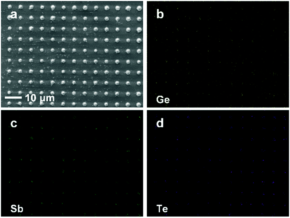 | ||
| Fig. 3 (a) SEM images showing regular arrays of GST-225 electrodeposited into nanostructured TiN electrodes (bottom contacts = 50 nm diameter, deposition time 50 s); (b)–(d) EDX element maps showing the deposition of Ge, Sb and Te onto only the lithographically exposed TiN regions of the substrates. | ||
The as-deposited GST film shows a similar Raman pattern to sputtered GST, with peaks positioned at 124 cm−1 and 142 cm−1, respectively as shown in Fig. 4a and b. The peak at 124 cm−1 can be attributed to the A1 mode of GeTe(4−n)Gen (n = 1, 2) corner-sharing tetrahedra.33–35 The 142 cm−1 peak, on the other hand, is believed to originate from the Sb–Te vibrations in SbTe3 units or from defective octahedral coordination of Sb atoms.35,36 The same peaks were observed from the GST in a single nanocell (Fig. 4b), suggesting that the composition of the GST remains the same on the nanoscale. EDX analysis (Fig. 4c) confirms that the composition of the film is very close to that expected for GST-225.
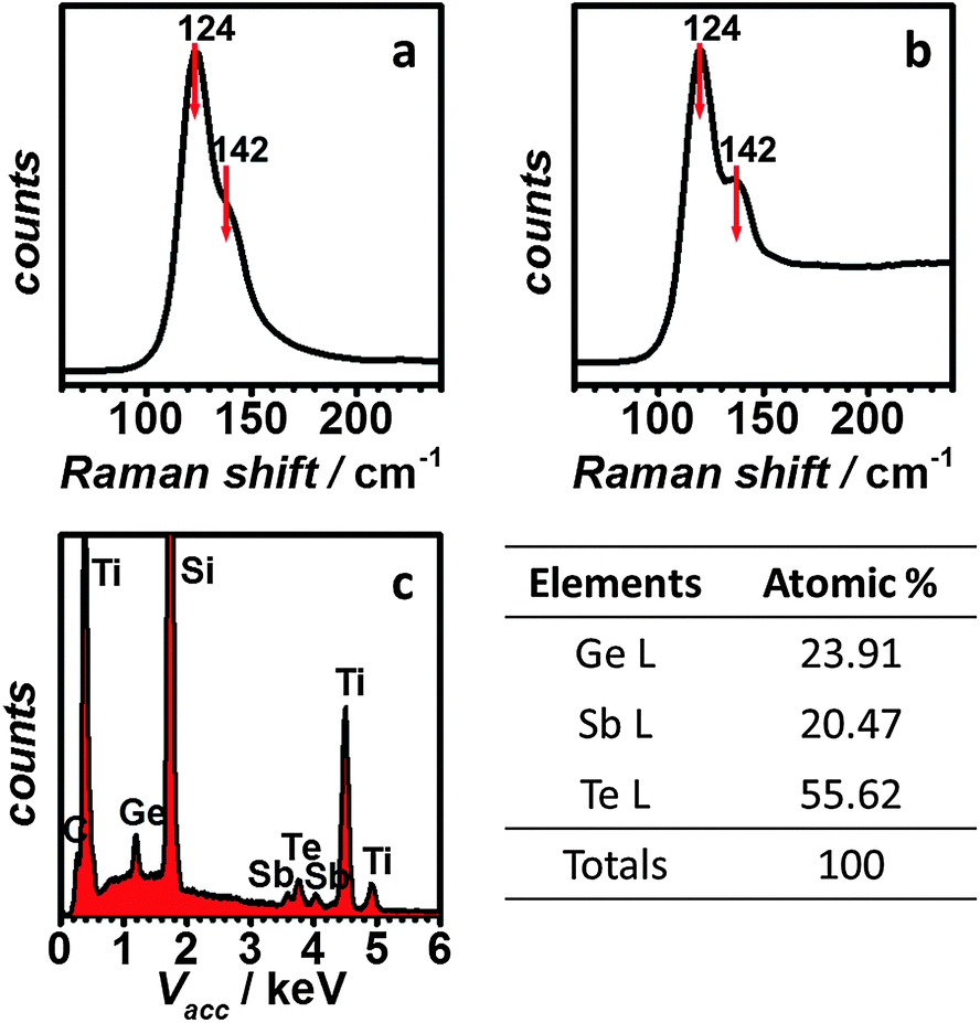 | ||
| Fig. 4 Raman spectra of (a) electrodeposited GST-225 thin film and (b) arrays of GST-225 electrodeposited into nanostructured TiN electrodes (bottom contacts = 50 nm diameter, deposition time 50 s); (c) EDX spectrum of electrodeposited GST-225 thin film. | ||
Diffraction patterns over a wider 2θ range (20–80°) for the thermally annealed thin films and for GST in 100 nm diameter e-beam patterned nanoarrays are shown in Fig. 5a and b. The deposited features are extremely uniform across the electrode, even for arrays with different cell densities (Fig. 5c).
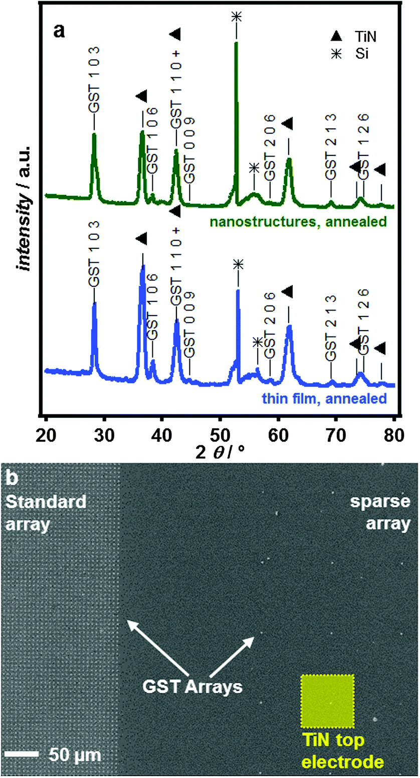 | ||
Fig. 5 (a) A comparison of the XRD patterns obtained on thermally annealed GST-225 deposited into 100 nm e-beam features and an annealed thin film. Stars (*) indicate Si features from the single crystalline Si substrate (varying by substrate orientation) and triangles (▲) indicate TiN peaks. GST indices are based on the stable P![[3 with combining macron]](https://www.rsc.org/images/entities/char_0033_0304.gif) m phase,32 though the structure of the 103 peak suggests multiple stacking sequences are present. (b) SEM image showing GST-225 electrodeposited into nanostructured TiN electrodes with a dense standard array for materials characterisation (left) and sparse array for electrical switching (right). The relative size of the TiN top electrode is also indicated in the Figure. m phase,32 though the structure of the 103 peak suggests multiple stacking sequences are present. (b) SEM image showing GST-225 electrodeposited into nanostructured TiN electrodes with a dense standard array for materials characterisation (left) and sparse array for electrical switching (right). The relative size of the TiN top electrode is also indicated in the Figure. | ||
The electrical memory switching properties of the electrodeposited GST thin films were investigated by fabricating vertical memory devices with TiN contacts on top of the GST film (Fig. 6a). The switching behaviour observed was reproducible for a large number of different devices. The I–V characteristics of a pristine GST memory device (Fig. 6b) display a high initial resistance (R ca. 8 MΩ), proving that the as-deposited GST is in the amorphous state. The high resistance remains until the voltage increases to the threshold value (ca. 3.5 V), where the current suddenly increases to the compliance value. The return sweep shows linear I–V behaviour with a resistance of ca. 3 kΩ, consistent with the material having been switched from the amorphous state to the conductive crystalline state. The threshold behaviour for the non-pristine device was investigated after resetting the device back to the amorphous state using an electrical pulse (6 V, 200 ns). Lower threshold voltages were observed with a uniform distribution around 1.3 V, indicating that a stable programming region had been formed within the device (Fig. 6c). The endurance performance of a cell based on an electrodeposited GST film was characterised with a set voltage pulse (Vset) of 2 V/1 ms and a reset voltage pulse (Vreset) of 6 V/200 ns (Fig. 6d). The device displays a stable endurance (>180 cycles) without failure, and the resistance ratio of reset to set states is maintained at ca. three orders of magnitude.6
 | ||
| Fig. 6 Memory switching characteristics of electrodeposited GST devices. (a) Schematic of the vertical GST devices and the electrical characterisation setup. (b) DC I–V sweep of a pristine GST device. (c) DC I–V sweeps of the non-pristine GST device. (d) Endurance characteristics of a GST device under cyclic voltage pulsing (set: 2 V, 1 ms; reset: 6 V, 200 ns). | ||
To establish the switching properties of nanoscale GST, nano-structured substrates accurately filled with GST are required to allow memory device fabrication. A cross sectional SEM image of GST electrodeposited into 100 nm wide trenches with a deposition time of 5 s shows some over-filling (Fig. 7a), however, complete filling (without overfilling) can be achieved when the deposition time was reduced to just 2 s (Fig. 7b). Memory cells based on the nano-structured GST were fabricated as illustrated in Fig. 7c. Fig. 7d illustrates programming erase cycles of a 100 nm GST memory cell switched between high- and low-resistance states repeatedly.
 | ||
| Fig. 7 Cross sectional SEM images of electrodeposited GST in 100 nm structures with deposition times of (a) 5 s and (b) 2 s, respectively. (c) Schematic of the nanostructured GST cells and the electrical characterisation setup. (d) Repeated resistance measurements of a 100 nm GST memory cell. | ||
The device set operation here was performed by DC sweeping (3 V), and the reset operation was accomplished with a 7 V, 200 ns pulse.
The electrical switching of the GST memory cells indicates that the GST material electrodeposited in this work retains good phase change properties even at the 100 nm scale. Therefore, this method proves to be capable of producing high quality materials which display electrical switching properties comparable to sputtered GST films, with the major added advantage that it can be used to form dense arrays of individual, insulated memory cells on the nm scale.
3. Conclusions
The electrodeposition of a device-quality ternary metal chalcogenide (GST-225) from a single, non-aqueous electrolyte system that provides fine control over the composition of the alloy by adjusting the electrolyte concentrations, has been demonstrated for the first time. The as-deposited GST-225 films are amorphous and exhibit annealing (crystallisation) behaviour as required for its application in solid-state memory applications. SEM, EDX, XRD, Raman and electrical switching experiments reveal that the PCM materials produced by this ‘bottom up’ approach are high quality, exhibiting a resistance contrast of three orders of magnitude between the amorphous and the crystalline phases, as well as very promising durability and switching lifetimes. This method is also shown to be entirely suitable for depositing the functional PCM material directly into patterned substrates, creating dense arrays of individual memory nano-cells. We have shown that highly uniform, switchable nano-structures of 50–100 nm diameter can be created over a large electrode area, providing a rapid and low-cost processing route. Switchable sub-10 nm cells are now a realistic prospect using this method.The electrodeposition of the demanding ternary GST alloy reported here clearly points towards the capability of our method to produce other semiconductor chalcogenide alloys with precise stoichiometric control and quality suitable for incorporation into electronic, thermoelectric and optical (nano)devices.
4. Experimental methods
Synthesis of precursors
The precursors [NnBu4][GeCl5], [NnBu4][SbCl4] and [NnBu4]2[TeCl6] were prepared and purified according to the literature methods.24,37Electrochemical characterisation
All electrochemical experiments and the electrolyte preparation were performed inside a glove box (Belle Technology) in order to exclude moisture and oxygen (<5 ppm). Electrolytes were prepared in anhydrous CH2Cl2 (previously dried by distillation from CaH2) using 0.1 mol dm−3 [NnBu4]Cl (Fluka, ≥99.0%, used without further purification) as the supporting electrolyte. The characterisation of the individual precursors was performed in electrolytes containing 1 × 10⁻² mol dm−3 of the relevant tetrabutylammonium chlorometallate. Ge2Sb2Te5 was deposited from an electrolyte containing 1 × 10⁻³ mol dm−3 [NnBu4][GeCl5], 1 × 10⁻³ mol dm−3 [NnBu4][SbCl4] and 2 × 10⁻³ mol dm−3 [NnBu4]2[TeCl6]. A Pt gauze was used as the counter electrode and for the reference electrode a home-made Ag/AgCl electrode, using 0.1 mol dm−3 [NnBu4]Cl in CH2Cl2 as the reference electrode electrolyte, was used. All experiments were performed in a standard one-compartment electrochemical cell within a wire mesh Faraday cage. A microAutolab 3 potentiostat and the Autolab Nova software package were used.Cyclic voltammetry was performed using glassy carbon working electrodes as they yielded data with less iR distortion than the TiN electrodes.24 Electrodeposition was performed on planar TiN substrates in order to provide a technologically relevant substrate. The preparation of the planar TiN substrates was discussed previously.24 Thin films of ca. 2 μm and 200 nm were prepared by controlling the amount of deposited material through the charge. On the 4 mm diameter electrode areas a charge of 0.5 C was passed for the 2 μm films and a charge of 0.05 C for the 200 nm films.
Film characterisation
The deposited GST films were investigated using scanning electron microscopy (SEM), energy dispersive X-ray (EDX) analysis, X-ray diffraction (XRD) and Raman spectroscopy. A Zeiss EVO LS 25 microscope equipped with an Oxford INCA x-act X-ray detector was used for the SEM and EDX analyses. High resolution SEM measurements were carried out with a field emission SEM (Jeol JSM 7500F). Films were imaged in high-vacuum mode. Annealing was performed using a rapid thermal annealler (Jipelec JetFirst) in a N2 atmosphere. XRD patterns were collected using a Rigaku SmartLab (9 kW) diffractometer (Cu-Kα1, or Cu-Kα for VT experiments), in grazing incidence configuration (θ1 = 1°). The temperature ramped XRD measurements were performed under a N2 atmosphere using an Anton Parr HTK Hot Stage. Raman scattering spectra were measured at room temperature on a Renishaw InVia Micro Raman Spectrometer using a helium-neon laser with a wavelength of 633 nm. The incident laser power was adjusted to ∼0.1 mW to minimise heating and consequent changes in the crystalline state or oxidation of the samples. The laser beam diameter on the sample was smaller than 2 μm using a 50× objective.Fabrication of GST Memory Cells
To minimise current leakage a 500 nm SiO2 insulating layer was first deposited on to a Si wafer by reactive sputtering of Si in an O2 atmosphere. A 200 nm thick TiN film was then reactively sputtered (Ti target in a N2 atmosphere) onto the SiO2 layer to form the bottom electrode (see ref. 9 for more details). This was followed by reactive sputtering of a second SiO2 layer. This layer of SiO2 was patterned into arrays of nanostructures using e-beam lithography (JEOL 9300FS) and subsequent etching in CHF3 and Ar (Oxford Instrument Plasmalab 80+). Both dense arrays and sparse arrays were patterned onto a single substrate for materials characterisation and electrical switching, respectively (see Fig. S5, ESI†). The electrodeposition conditions were identical to those used in the preparation of the planar films with the exception that the thickness of the material deposited into the nanopatterned substrates was controlled by the deposition time. Both thin film devices and nanostructured memory cells were then formed by patterning TiN top electrodes. A 200 nm TiN film was reactively sputtered onto the substrate after GST electrodeposition. The top electrodes (50–100 μm in size) were then defined by photolithography and subsequent etching with Cl2 (Oxford Instruments System 100 ICP 380).Electrical measurements
All electrical measurements were performed with a Keithley 4200 semiconductor characterisation system. During the measurements, the programming voltage bias was applied to the top electrode, while keeping the bottom electrode grounded. The probe/point contacts to the top and bottom electrodes of the devices were realised through a pair of Wentworth probe needles, using a Wentworth laboratories AVT 702 semi-automatic prober. For electrical pulsing, two ns-pulsing measuring units (PMUs) were integrated within the same characterisation setup. The resistance of the devices after applying set or reset voltage pulses was measured at 0.1 V (DC).Acknowledgements
We thank the EPSRC for support (EP/I010890/1) and for provision of the thin film X-ray diffraction instrument (EP/K009877/1 and EP/K00509X/1), and the Royal Society for a Wolfson Merit Award (PNB). We also thank Mr G. Purdy and Dr S. Guerin (Ilika plc) for helpful discussions and Dr M. Jura and Dr G. Stenning (ISIS at STFC, UK) for assistance with the temperature ramped XRD experiments.Notes and references
- B. Poudel, Q. Hao, Y. Ma, Y. Lan, A. Minnich, B. Yu, Z. Yan, D. Wang, A. Muto, D. Vashaee, X. Chen, J. Liu, M. S. Dresselhaus, G. Chen and Z. Ren, Science, 2008, 320, 634 CrossRef CAS PubMed.
- J. Xu, X. Yang, H. Wang, X. Chen, C. Luan, Z. Xu, Z. Lu, V. A. L. Roy, W. Zhang and C.-S. Lee, Nano Lett., 2011, 11, 4138 CrossRef CAS PubMed.
- M.-R. Gao, Y.-F. Xu, J. Jiang and S.-H. Yu, Chem. Soc. Rev., 2013, 42, 2986 RSC.
- M. J. Polking, J. J. Urban, D. J. Milliron, H. Zheng, E. Chan, M. A. Caldwell, S. Raous, C. F. Kisielowski, J. W. Ages III, R. Ramesh and A. P. Alivisatos, Nano Lett., 2011, 11, 1147 CrossRef CAS PubMed.
- J. J. Cha, K. J. Koski, K. C. Y. Huang, K. X. Wang, W. Luo, D. Kong, Z. Yu, S. Fan, M. L. Brongersma and Y. Cui, Nano Lett., 2013, 13, 5913 CrossRef CAS PubMed.
- S. Raoux, W. Wełnic and D. Ielmini, Chem. Rev., 2010, 110, 240 CrossRef CAS PubMed.
- Y. Fujisaki, Jpn. J. Appl. Phys., 2010, 49, 100001 CrossRef.
- M. Wuttig and N. Yamada, Nat. Mater., 2007, 6, 824 CrossRef CAS PubMed.
- D. Ielmini and A. L. Lacaita, Mater. Today, 2011, 14, 600 CrossRef CAS.
- H. S. P. Wong, S. Raoux, S. Kim, J. L. Liang, J. P. Reifenberg, P. Rajendran, M. Asheghi and K. E. Goodson, Proc. IEEE, 2010, 98, 2201 CrossRef.
- M. Schlesinger and M. Paunovic, Modern Electroplating, John Wiley & Sons, 4th edn, 2000 Search PubMed.
- P. C. Andricacos, C. Uzoh, J. O. Duckovic, J. Horkans and H. Deligianni, IBM J. Res. Dev., 1998, 42, 567 CrossRef CAS.
- K. Fukami, Y. Tanaka, M. L. Chourou, T. Sakka and Y. H. Ogata, Electrochim. Acta, 2009, 54, 2197 CrossRef CAS PubMed.
- J. Ke, W. Su, S. M. Howdle, M. W. George, D. Cook, M. Perdjon-Abel, P. N. Bartlett, W. Zhang, F. Cheng, W. Levason, G. Reid, J. Hyde, J. Wilson, D. Smith, K. Mallik and P. Sazio, Proc. Natl. Acad. Sci. U. S. A., 2009, 106, 14768 CrossRef CAS PubMed.
- P. N. Bartlett, D. A. Cook, M. W. George, A. L. Hector, J. Ke, W. Levason, G. Reid, D. C. Smith and W. Zhang, Phys. Chem. Chem. Phys., 2014, 16, 9202 RSC.
- Electrodeposition from Ionic Liquids, ed. F. Endres, D. MacFarlane and A. Abbott, Wiley-VCH, Chichester, 2008 and references therein Search PubMed.
- W. Simka, D. Puszczyk and G. Nawrat, Electrochim. Acta, 2009, 54, 5307 CrossRef CAS PubMed.
- W. J. Wang, L. P. Shi, R. Zhao, K. G. Lim, H. K. Lee, T. C. Chong and Y. H. Wu, Appl. Phys. Lett., 2008, 93, 043121 CrossRef PubMed.
- X. M. Long, X. S. Miao, J. J. Sun, X. M. Cheng, H. Tong, Y. Li, D. H. Yang, J. D. Huang and C. Liu, Solid-State Electron., 2012, 67, 1 CrossRef CAS PubMed.
- T. Eom, S. Choi, B. J. Choi, M. H. Lee, T. Gwon, S. H. Rha, W. Lee, M.-S. Kim, M. Xiao, I. Buchanan, D.-Y. Cho and C. S. Hwang, Chem. Mater., 2012, 24, 2099 CrossRef CAS.
- A. G. Schrott, C.-F. Chen, M. J. Breitwisch, E. A. Joseph, R. K. Dasaka, R. W. Cheek, Y. Zhu and C. Lam, Mater. Res. Soc. Symp. Proc., 2010, 1251, H06 CrossRef.
- V. Venkatasamy, I. Shao, Q. Huang and J. L. Stickney, J. Electrochem. Soc., 2009, 155, D693 CrossRef PubMed.
- X. Liang, N. Jayaraju, C. Thambidurai, Q. Zhang and J. L. Stickney, Chem. Mater., 2011, 23, 1742 CrossRef CAS.
- P. N. Bartlett, D. Cook, C. H. de Groot, A. L. Hector, R. Huang, A. Jolleys, G. P. Kissling, W. Levason, S. J. Pearce and G. Reid, RSC Adv., 2013, 3, 15645 RSC.
- G. Reid, P. N. Bartlett and A. L. Hector, PCT/GB2013/000322, WO 2014/016544 A2, 2014.
- F. Endres and S. Z. El Abedin, Chem. Commun., 2002, 892 RSC.
- R. Al-Salman, S. Z. El Abedin and F. Endres, Phys. Chem. Chem. Phys., 2008, 10, 4650 RSC.
- F. Endres, Phys. Chem. Chem. Phys., 2001, 3, 3165 RSC.
- P. N. Bartlett, C. Y. Cummings, W. Levason, D. Pugh and G. Reid, Chem. – Eur. J., 2014, 20, 5019 CrossRef CAS PubMed.
- J. Ke, P. N. Bartlett, D. Cook, T. L. Easun, M. W. George, W. Levason, G. Reid, D. Smith, W. Su and W. Zhang, Phys. Chem. Chem. Phys., 2012, 14, 1517 RSC.
- P. Urban, M. N. Schneider, L. Erra, S. Weizmiller, F. Fahmbauer and O. Oeckler, CrystEngComm, 2013, 15, 4823 RSC.
- S. Raoux, J. L. Jordan-Sweet and A. J. Kellock, J. Appl. Phys., 2008, 103, 114310 CrossRef PubMed.
- G. C. Sosso, S. Caravati, R. Mazzarello and M. Bernasconi, Phys. Rev. B: Condens. Matter Mater. Phys., 2011, 83, 134201 CrossRef.
- S. Kozyukhin, M. Veres, H. P. Nguyen, A. Ingram and V. Kudoyarova, Phys. Procedia, 2013, 44, 82 CrossRef CAS PubMed.
- P. Nmec, V. Nazabal, A. Moreac, J. Gutwirth, L. Beneš and M. Frumar, Mater. Chem. Phys., 2012, 136, 935 CrossRef PubMed.
- P. Nmec, A. Moreac, V. Nazabal, M. Pavlista, J. Prikryl and M. Frumar, J. Appl. Phys., 2009, 106, 103509 CrossRef PubMed.
- I. R. Beattie, T. Gilson, K. Livingston, V. Fawcett and G. A. Ozin, J. Chem. Soc. A, 1967, 712 RSC.
Footnote |
| † Electronic supplementary information (ESI) available: Describes the method used to approximate the film thickness based upon the charge passed. See DOI: 10.1039/c5mh00030k |
| This journal is © The Royal Society of Chemistry 2015 |