
Charge selective contacts, mobile ions and anomalous hysteresis in organic–inorganic perovskite solar cells†
Ye
Zhang‡
ab,
Mingzhen
Liu‡
a,
Giles E.
Eperon
a,
Tomas C.
Leijtens
ac,
David
McMeekin
a,
Michael
Saliba
a,
Wei
Zhang
a,
Michele
de Bastiani
c,
Annamaria
Petrozza
c,
Laura M.
Herz
a,
Michael B.
Johnston
*a,
Hong
Lin
*b and
Henry J.
Snaith
*a
aUniversity of Oxford, Department of Physics, Clarendon Laboratory, Parks Road, Oxford, UK. E-mail: h.snaith1@physics.ox.ac.uk; m.johnston@physics.ox.ac.uk
bState Key Laboratory of New Ceramics & Fine Processing, School of Materials Science and Engineering, Tsinghua University, Beijing 100084, P. R. China. E-mail: hong-lin@tsinghua.edu.cn
cCenter for Nano Science and Technology@PoliMi, Istituto Italiano di Tecnologia, Via Pascoli 70/3, 20133 Milano, Italy
First published on 4th March 2015
Abstract
High-efficiency perovskite solar cells typically employ an organic–inorganic metal halide perovskite material as light absorber and charge transporter, sandwiched between a p-type electron-blocking organic hole-transporting layer and an n-type hole-blocking electron collection titania compact layer. Some device configurations also include a thin mesoporous layer of TiO2 or Al2O3 which is infiltrated and capped with the perovskite absorber. Herein, we demonstrate that it is possible to fabricate planar and mesoporous perovskite solar cells devoid of an electron selective hole-blocking titania compact layer, which momentarily exhibit power conversion efficiencies (PCEs) of over 13%. This performance is however not sustained and is related to the previously observed anomalous hysteresis in perovskite solar cells. The “compact layer-free” meso-superstructured perovskite devices yield a stabilised PCE of only 2.7% while the compact layer-free planar heterojunction devices display no measurable steady state power output when devoid of an electron selective contact. In contrast, devices including the titania compact layer exhibit stabilised efficiency close to that derived from the current voltage measurements. We propose that under forward bias the perovskite diode becomes polarised, providing a beneficial field, allowing accumulation of positive and negative space charge near the contacts, which enables more efficient charge extraction. This provides the required built-in potential and selective charge extraction at each contact to temporarily enable efficient operation of the perovskite solar cells even in the absence of charge selective n- and p-type contact layers. The polarisation of the material is consistent with long range migration and accumulation of ionic species within the perovskite to the regions near the contacts. When the external field is reduced under working conditions, the ions can slowly diffuse away from the contacts redistributing throughout the film, reducing the field asymmetry and the effectiveness of the operation of the solar cells. We note that in light of recent publications showing high efficiency in devices devoid of charge selective contacts, this work reaffirms the absolute necessity to measure and report the stabilised power output under load when characterizing perovskite solar cells.
Conceptual insightsThis work emphases the necessity to incorporate charge selective contacts in organic–inorganic perovskite solar cell structures by demonstrating that despite apparent measured power conversion efficiency of 11% and 13.2% obtained from current–voltage scans under simulated sun light, which is a routine measurement to evaluate solar cells, devices devoid of a titania compact layer exhibit very low stabilised power output of 2.7% for standard mesoporous cells and approximately zero for the planar ones. This unsustainable photovoltaic performance is found to be related to the previously observed anomalous hysteresis in perovskite solar cells, i.e. efficiency variation depending on measuring protocols. Further, this work contains new insights into device designs which advances the understanding relating to the perovskite material property. The proposed mechanism involving a bias induced doping gradient provides useful information with regard to the underlying mechanism associated with mobile charged species. Lastly, a framework for correctly evaluating the performance of perovskite solar cells is put forward to standardize future measurement protocol and report reliable photovoltaic performance in this field. |
Introduction
Research into organic–inorganic metal halide perovskite solar cells CH3NH3PbX3 (X = Cl, Br, I) has swiftly gained momentum since the seminal work by Kojima et al. in 2009, and the realisation of highly efficient solid-state perovskite solar cells in 2012 and 13,1–7 with certified power conversion efficiencies of over 20% already having been achieved,8,9 due to excellent properties of the perovskite materials such as high optical coefficient, tunable bandgap, long diffusion length, and high ambipolar charge carrier mobility,10,11 perovskite materials have been widely investigated in two solar cell configurations, i.e. thin-film and mesostructured architectures. In most of the previously reported research, an n-type compact layer (mostly TiO2) is employed to ensure selective extraction of electrons at the anode contact, adopted from dye-sensitized solar cells,12 with several recent approaches achieving low-temperature processing of the compact TiO2 in well-performing devices.13–15 In the original embodiment of a thin film perovskite solar cell, a solid layer of the perovskite is coated on top of the compact TiO2, which is then coated by a p-type hole transporter.3,16–18 A complementary, rapidly advancing approach is to “invert” the original architecture and coat the perovskite upon a p-type organic hole-conductor (for example PEDOT:PSS or nickel oxide) and subsequently coat an electron selective charge collection layer on top of the perovskite, typically phenyl-C61-butyric acid methyl ester (PCBM) or C60.19–21 Of high relevance, these inverted perovskite solar cells with all organic contacts generally exhibit little hysteresis.In a “mesostructured” architecture, a typical device consists of the perovskite material infiltrated into a TiO2 or Al2O3 mesostructure, with an additional solid capping layer of perovskite on top, all sandwiched between the hole-blocking electron extracting TiO2 compact layer and an electron-blocking, hole transport material (HTM).6,7,11,13,22 The double layered, mesoporous, with solid perovskite capping layer, structure appears to be prevalent in many of the most efficient devices. Recently, we have observed that the Fermi level of the perovskite material is raised closer to the conduction band in the perovskite when it is infiltrated into an alumina or titania scaffold.6 The metal oxide scaffold hence provides an effective n-doping in this layer, likely resulting in a favourable n-type/intrinsic homo junction within the perovskite layer.23 We note that the origin of the effective n-doping is not yet fully understood, but may be due to under-coordinated halides acting as shallow electron donors on the crystal surface, or due to a surface charge effect of the mesoporous metal oxide.
There have been a number of recent observations that the measuring protocol and voltage bias history alters the photovoltaic behaviour, the shape of the current voltage curve and hence the derived PCEs for perovskite solar cells.24–26 We thus suggested that the stabilised maximum power output measured under working conditions is a critical indicator to fully evaluate device performance. Preliminary studies showed that planar heterojunction devices usually suffer from more severe hysteresis and consequently lower stabilised maximum power output than their mesoporous counterpart.24 Herein, we explore the possibility and impact of fabricating perovskite solar cells entirely free of an electron selective charge collection layer. Counter-intuitively, but consistent with some recent reports,27–29 we achieve 11.0% and 13.2% J–V curve derived PCE for planar heterojunction and mesoporous alumina compact layer-free devices, but with substantial hysteresis in the J–V curves.24 We carry out a detailed study to probe the stabilised PCE of the fabricated devices holding them under constant voltage near the maximum power point of the J–V curve under simulated solar illumination. We observe that the devices stabilise at a dramatically lower PCE than their apparent J–V derived PCE, with the stabilised power output approaching zero for the planar structure in the absence of an electron selective contact. We use this information, along with further characterisation of both planar and mesostructured architectures, to greatly enrich our understanding and propose a phenomenological model for hysteresis and temporally changing properties of perovskite solar cells.
Results and discussion
We fabricated planar and mesostructured CH3NH3PbI3−xClx perovskite solar cells both with and without a titania compact layer and/or hole-transporting layer. The perovskite, optionally infiltrated within a mesoporous alumina scaffold, is sandwiched between fluorine-doped tin oxide (FTO), with or without a titania compact layer (henceforth Ti-CL), and with or without a hole transporting material 2,2′,7,7′-tetrakis-(N,N-di-p-methoxyphenylamine)9,9′-spirobifluorene (spiro-OMeTAD) doped with lithium bis(trifluoromethylsyfonyl)imide (Li-TFSI) and tert-butylpyridine (tBP), as we show in Fig. 1. Uniform, planar films were formed as described by Eperon et al.16 though we note that the films fabricated on the Ti-CL free devices were not as uniform as those processed on the Ti-CLs. As we show in Fig. 1d and h, in the mesoporous devices, there exists a significant capping layer of perovskite on top of the perovskite/alumina infiltrated layer.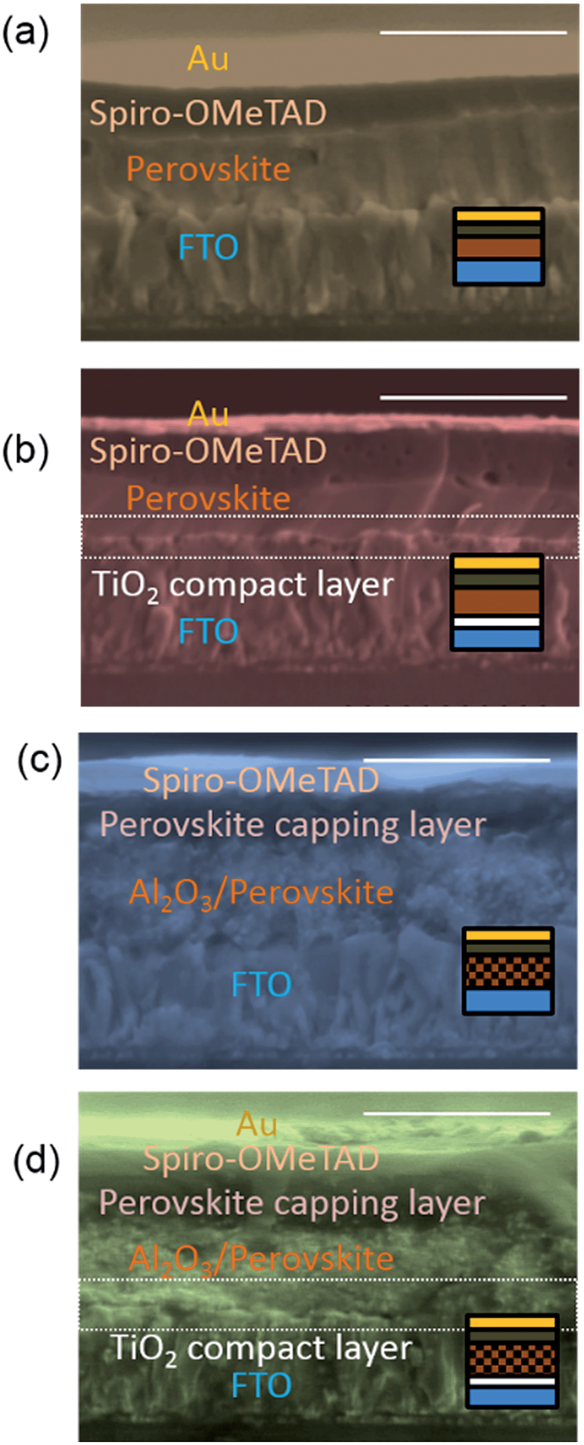 | ||
| Fig. 1 Device structure and SEM images of CH3NH3PbI3−xClx perovskite solar cells. (a) Planar structure without a titania compact layer. (b) Planar structure with a titania compact layer. (c) Mesoporous structure on an Al2O3 scaffold without a titania compact layer. (d) Mesoporous structure on an Al2O3 scaffold with a titania compact layer. The diagrams indicate cross-sections of each device. The scales indicate 1 μm. | ||
Firstly, we examined devices with or without a Ti-CL, but always containing an organic HTM layer. We show the solar cell performances of the best devices fabricated of each architecture in Fig. 2 and Table 1 (averaged data is tabulated in Table S1†). The best planar device with a Ti-CL exhibited a PCE of 14.2%, a Jsc of 22.8 mA cm−2 and Voc of 0.88 V in the forward bias to short-circuit (FB–SC) scan. Upon removal of the Ti-CL, we obtained a PCE of up to 11.5%, with a Jsc of 19.5 mA cm−2 and a Voc of 0.95 V derived from the FB–SC scan. The FF drops from 0.70 to 0.62. Reversing the scan direction from SC (short circuit) to FB (forward bias) resulted in a considerable drop in Voc and FF, due to the device hysteresis.24 It is impressive that devices absent of the Ti-CL still appear to produce such efficiencies – if recombination at the FTO–perovskite interface was critical, we would expect much lower Voc and FF. However, we only observe a small drop in performance in the FB–SC scan indicating that selective electronic contact to the quasi Fermi levels for electrons in the perovskite, is possible from the FTO.
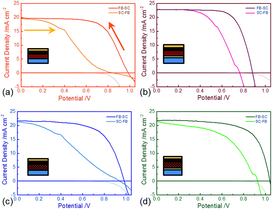 | ||
| Fig. 2 Forward bias to short-circuit (FB–SC) and SC–FB J–V curves of perovskite solar cells with different structures measured under simulated AM1.5, 100 mW cm−2 solar irradiance of the best performing solar cells for each type. Devices are scanned at 0.38 V s−1 after holding the devices at 1.4 V forward bias under illumination for 5 seconds. (a) Planar structure without a titania compact layer, (b) planar structure with a titania compact layer. (c) Mesoporous structure on an Al2O3 scaffold without a titania compact layer, (d) mesoporous structure on an Al2O3 scaffold with a titania compact layer. Corresponding dark currents (FB–SC) are plotted underneath the x-axis. The arrows indicate the scan directions. The inserted diagrams indicate cross-sections of each device configuration. | ||
| Device structures | Ti-CL | HTM | Scan direction | J sc (mA cm−2) | V oc (V) | FF (%) | Dark current onset (V) | Highest PCE (%) | PCE std deviation (%) | Stabilised PCE (%) |
|---|---|---|---|---|---|---|---|---|---|---|
| Planar | No | Yes | FB–SC | 19.54 | 0.95 | 0.62 | 0.84 | 11.5 | 5.69 ± 2.49 | 0 |
| SC–FB | 19.50 | 0.80 | 0.41 | 6.4 | ||||||
| Planar | Yes | Yes | FB–SC | 22.8 | 0.88 | 0.70 | 1.1 | 14.2 | 9.22 ± 3.18 | 9.12 |
| SC–FB | 22.9 | 0.76 | 0.54 | 9.5 | ||||||
| Meso | No | Yes | FB–SC | 21.68 | 1.00 | 0.62 | 1.1 | 13.2 | 8.86 ± 2.31 | 2.7 |
| SC–FB | 21.31 | 0.95 | 0.33 | 6.5 | ||||||
| Meso | Yes | Yes | FB–SC | 21.79 | 1.04 | 0.66 | 1.05 | 15.5 | 11.32 ± 2.68 | 13.5 |
| SC–FB | 21.47 | 0.93 | 0.51 | 10.6 | ||||||
| Planar | No | No | FB–SC | 7.11 | 0.77 | 0.53 | 0.7 | 3.2 | 0 | |
| Meso | No | No | FB–SC | 18.6 | 0.80 | 0.47 | 0.7 | 7.1 | 0 |
When we introduce a mesoporous Al2O3 scaffold layer into the device, we observe slightly better reproducibility (Fig. 2 below). We achieve a PCE of over 15%, with a Jsc of 21.8 mA cm−2, a Voc of 1.04 V and a FF of 0.66 in the FB–SC scan. Removal of the Ti-CL only leads to a slight decrease in FF and open-circuit voltage on the FB–SC J–V scan, and a slightly larger drop in performance parameters on the SC–FB scan.
As we have previously shown,24 we observed that significant hysteresis occurs even in standard device structures with Ti-CL. The hysteresis for the cells fabricated with the absence of Ti-CL is exaggerated, but not overtly. In order to determine the ‘real’ sustained device performance under working conditions we apply a constant bias close to the maximum power point voltage determined from the FB–SC J–V curve, and measure the current output under simulated sun light. We show the current and power output for the different device architectures in Fig. 3. Strikingly, despite the apparently relatively similar behaviour in the fast J–V scan, the control mesoporous samples with compact TiO2 stabilise close to the PCE determined by the FB–SC J–V scan at 13.5%, but the Ti-CL-free mesoporous cells stabilise at a much lower value of only 2.7%. The Ti-CL-free planar cells generate approximately zero sustained current density and PCE. This reveals that perovskite photovoltaic diodes fabricated without an electron selective layer are not suitable for generating sustained power.
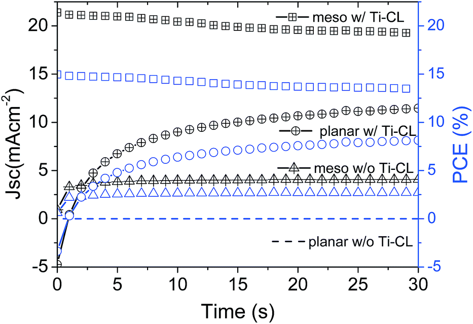 | ||
| Fig. 3 stabilised maximum power output PCE data (blue open symbols) and current density (black open symbols with crosses) of perovskite solar cells with and without Ti-CL. Dashed lines indicate Ti-CL free planar samples; hollow square symbols indicate standard mesoporous samples; triangles indicate mesoporous samples without Ti-CL; hollow circular symbols indicate planar samples with Ti-CL. Note all the devices investigated here were fabricated with the HTM layer. The current density and stabilised PCE of planar devices w/o Ti-CL, shown as dashed lines, are essentially zero and overlap with each other. | ||
There are a number of interesting observations that we can extract from this data. Firstly, it is clear that there is a short-lived effect (beneficial during FB–SC scan and yet disadvantageous during the SC–FB scan) responsible for hysteresis in these devices, which then disappears during the stabilised power scan. This is enabled by the 5 second “pre-biasing” at 1.4 V forward bias, and appears to dissipate entirely on a time scale slower than the J–V scan (seconds). In the case of the cells with Ti-CL, this phenomena is not critical to obtaining reasonable stabilised output, though it does appear to temporarily enhance the fast scan efficiency compared to the stabilised output. In the case of the cells with no Ti-CL, the stabilised PCE is much further reduced compared to the fast scan PCE. Secondly, we observe that the Ti-CL free planar cells have almost zero stabilised power output, and the Ti-CL mesostructured cells do still generate some power. As such, these results highlight that the benefit of the alumina scaffold does not just lie in its effect on film formation.
We have previously shown evidence that the perovskite material infiltrated within the mesostructure is effectively n-doped, despite the absence of an impurity dopant, and the capping layer or planar perovskite layer is approximately intrinsic.30 In this light, the mesostructured cells with no Ti-CL would in fact have an n–i homojunction in contact with the p-type hole conductor, thus providing a permanent built-in field to the device, which would enable stabilised charge extraction at maximum power point even in the absence of an electron selective heterojunction. The Ti-CL free planar cells would effectively be an intrinsic layer in contact with the metallic FTO, and form an i–p heterojunction with the hole transporter.
One other way to probe whether there is indeed a built-in field caused by a difference in Fermi level of the n–i homojunction in the region between the mesostructured and solid perovskite capping layer is to simply put symmetric contacts on either side of the junction and probe if there is photocurrent when the device is short-circuited. In the case where there is substantial photocurrent, there must be a field driving the photo-generated electrons and holes to opposite contacts. Here, we deposited planar, meso-superstructured, and meso-superstructured devices with a perovskite capping layer on top of a gold contact. We contact the cells on the top with another semitransparent gold contact (25 nm thick) to complete the device. We then irradiated the sample with modulated (123 Hz) laser light (690 nm at a maximum fluence of 1.5 × 1018 cm−2), and the photocurrent at short-circuit was monitored with a lock-in amplifier phased to the modulated excitation. We plot the results in Fig. 4a. It is apparent that while the planar and meso-superstructured samples display almost negligible photocurrents regardless of the fluence, the meso-superstructured samples with a capping layer display a photocurrent increasing linearly with light intensity, with electrons being collected at the gold/Al2O3 contact and holes at the gold/capping layer contact. This photocurrent is two orders of magnitude larger than that for the other structures. This is direct evidence that there is indeed a field across such a device, and that this field is in a direction beneficial to charge collection in the solar cell, consistent with our observations that Ti-CL free meso-superstructured solar cells with a capping layer can deliver a sustained, albeit low, power output.23
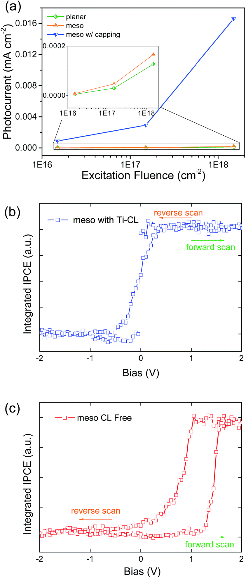 | ||
| Fig. 4 (a) photocurrent vs. excitation fluence on planar, meso-structured, meso-structured with capping layer devices. Inset: enlarged photocurrent of planar and meso-structured devices. (b) and (c) IPCE loops based on FTPS measurement. | ||
To further investigate the transient photovoltaic behaviour we probed the charge extraction at short-circuit of both standard meso-structured devices with a perovskite capping layer, and Ti-CL free mesoporous cells (with spiro-OMeTAD on). The cells were subjected to an increasing forward bias for a fixed duration (20 seconds), with the photocurrent spectra at short-circuit rapidly recorded between bias steps, employing Fourier Transform Photocurrent Spectroscopy (FTPS). FTPS is a spectroscopic method where a monochromator is replaced by a Fourier Transform Infrared spectrophotometer (FTIR). In such a measurement, light of a single wavelength is not isolated but encoded in a full spectrum so that all wavelengths can illuminate simultaneously; it can subsequently be mathematically decoded to yield spectral distribution.31,32 FTPS makes a powerful tool to probe the alternation of device operation brought by transient changes to the selective contacts, as we have observed, since the integrated IPCE can be performed on short timescales (∼0.1 s). We pre-bias the devices at differing biases and perform integrated IPCE immediately after the devices are switched to short-circuit. Ideally if biasing does not essentially change the device operating nature, the integrated IPCE would remain constant regardless of biasing field and time, or sweep direction.
Notably, both devices exhibit non-appreciable short-circuit photocurrent following reverse biasing. As we show in Fig. 4, with a small amount of forward biasing the standard meso-structured device with a Ti-CL exhibits an immediate rise to the steady maximum current value, indicating the ability to generate close to full photocurrent in the power quadrant of the solar cell J–V curve. The return sweep, stepping from forward bias back towards reverse bias, approximately overlaps with the reverse to forwards bias scan showing almost identical integrated IPCE (Fig. 4b). In contrast, the removal of Ti-CL leads to a much slower ascent when stepping the bias, and the solar cell needs to be heavily forward biased before the “saturated photocurrent” is achieved. This means that under the J–V maximum power point voltage, the photocurrent will be much lower than the maximum attainable with pre-biasing. We note that the apparent “hysteresis” loop in this measurement protocol is due to the finite rest time of 20 s per bias step, and with fully stabilised slow steps we expect this to disappear.
As a final probe of the nature of the pre-biasing effect, we fabricated planar and mesoporous devices that only consist of the perovskite material and metallic contacts, i.e., without Ti-CL or spiro-OMeTAD. We show in the SI that despite the absence of either an electron or hole transporting layer, the cells still displayed apparent fast scan FB–SC PCEs of 3.2% and 7.1%, respectively (Fig. S1†). Unsurprisingly, similar to the case of Ti-CL free samples with the HTM, these devices produce negligible power output when held at their maximum power point voltage.
At this point, it is useful to take a step backwards and ask the question; how do the perovskite solar cells work at all (even if temporarily) without an electron selective contact? It is well known that materials can operate in solar cells with direct metal contact to the semiconductor, but efficient solar cell operation can only occur if there is a presence of built-in fields, an asymmetry in the field distribution through the device. As such, it seems likely that we must be inducing in our perovskite devices a temporary polarisation, which results in a field asymmetry, allowing functional device operation until the effect relaxes. We propose that motion of ions, either vacancies or interstitials, is responsible for the temporary polarisation observed. We can rule out electron/hole motion due to the timescales involved (seconds). Ferroelectric contributions have also been proposed as a mechanism for hysteresis, but we believe (an in-depth study to be published separately) that the dependence of the polarisation with voltage and frequency is not consistent with ferroelectric domain rearrangements.33,34 Although a giant permittivity has been proposed to be relevant to the hysteretic effect, it cannot be responsible for inducing a built-in field.35 The apparent giant permittivity observed previously could in fact be explained by the ionic motion model we propose hereby.
We illustrate our proposed mechanism in Fig. 5. Consider the perovskite semiconductor, containing positive and negatively charged ionic species, to be contacted on either side by metal electrodes (Fig. 5a). When the device is under forward bias, instantaneously there will be a field drop uniformly across the perovskite layer (Fig. 5b). If there are mobile ionic species present within the perovskite film, these species will migrate towards the appropriate electrode to compensate the electric field in regions close to the electrodes (Fig. 5c).36 This could be for instance by positive ions or ionic species migrating to the anode, and negative ions migrating to the cathode. This situation, as illustrated in Fig. 5c, would be almost identical to that in a light emitting electrochemical cell under operation of charge injection, where the electric field is enhanced near the electrodes.37,38 Once the external field is released, and a large fraction of charge are photogenerated within the perovskite film, these displaced ions will enable the stabilisation of a high density of space charge near each of the contacts, n near the electron selective contact and p near the hole selective contact. This is equivalent to n and p-doping near the charge collection interfaces, providing a band bending near the contacts (Fig. 5d). This is the ‘good’ state in which even the selective contact-free devices function efficiently. Over time however, the mobile ions will diffuse back throughout the perovskite film until they are evenly distributed, and the solar cells will once again have to operate without the benefit of this temporary doping near the electrodes. This mechanism would mean that by pre-biasing the device before measuring, we can obtain what is effectively the best possible device attainable with the perovskite material used, regardless of contact layers. Only under steady state holding bias can we measure the actual power output of the device including the effects of the contact layers. Notably, if the device is biased in the reverse direction, this model would predict an accumulation of hole density near the electron collection electrode and electron dentistry near the hole collection electrode, disadvantageous for efficient solar cell operation.
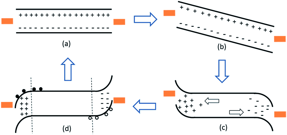 | ||
| Fig. 5 Schematic illustration of the migration of ionic species, giving a beneficial temporary photovoltaic performance after subjecting the cells to forward bias. For simplicity this diagram assumes symmetric metallic contacts and makes no judgement upon any interactions between the perovskite and the metal contacts. In (a) there is no field across the device and mobile ionic species are uniformly distributed. Instantaneously following the application of an external bias, there will be an electric field drop uniformly across the film, since the ions have no time to migrate. After a certain time period, in (c) the mobile ionic species have migrated in the appropriate direction and screened the electric field to regions closest to the interface. After removing the external bias and exposing the device to light, in (d) the ions have not had time to re-disperse and photogenerated free carriers will associate with the net negative and positive ionic species in the regions near the contacts. This will have the same effect as impurity doping and result in n-type doping near the anode (left) and p-type doping near the cathode (right). After a certain period of time (back to (a)) the ions will redistribute throughout the film and the interfacial doping will dissipate. | ||
Previous findings add weight to our proposed mechanism; Xiao et al. have recently demonstrated switchable photocurrent in symmetrical perovskite devices explained by a similar mechanism of ion motion, and reinforced this theory by monitoring compositional change at the electrodes.39 Their devices are reversibly polarisable (until the material composition changes permanently), showing hysteretic behaviour with changing bias direction, as we would expect. Moreover, the effect of ionic motion to compensate an applied field is well-known in the field of light-emitting electrochemical cells.37 A very similar mechanism to that which we have outlined is thought to be responsible for efficient operation of these devices, which consist of an emitting ion conductive layer in between two metallic contacts. Only when sufficient bias is applied to cause significant ionic motion, does charge injection become efficient and such devices display high luminescent efficiency.40 Since halide perovskites are well-known as ion conductors, this reinforces our argument for ionic motion as the hysteretic mechanism.41
We note that there are likely to be more complexities in the real device operations than the simple model outlined here, and the exact evolution of electric field distribution throughout the film required in depth mathematical modelling. In addition, if enough ions move, the stoichiometry of the film near the contacts could change. It has been observed that changing the precise composition of the film can lead to self-doping;35,36 a distribution of methylammonium and iodide ions across the film could provide a doping gradient, or strongly doped regions at the contacts. This could also be relevant for explaining the improved solar cell operation. We note that we do not present evidence here for concluding the precise mechanism by which ionic drift is likely to affect device operation.42,43 In addition to the macroscopic effect of a temporary built-in field forming, it is plausible that there are interface-specific effects – mobile ions could passivate traps or defect states at the interface, for example. Finally, although we conclude that ion drift is likely to be a dominant effect, other dynamic processes with different timescales, such as molecular dipole reorientation and lattice distortion (octahedral titling) could also occur.34,44,45
For completeness, we summarise the difference in operation between the cells with and without charge selective contacts. In the case of the perovskite cells incorporating Ti-CLs, resulted charge accumulation near the contacts temporarily enables selective collection of charge at the contacts, leading to the enhanced ‘fast scan’ FB–SC determined efficiencies. The stabilised PCE is only slightly lower because the selective contacts operate reasonably but not perfectly well on their own. In the Ti-CL-free planar devices, which have no inherent selectivity for electron collection, the temporary effect enables them to function, however only transiently. In the Ti-CL-free mesostructured devices, which have a (presumably relatively small) built-in field arising from the n-doped perovskite infiltrated within the alumina and the intrinsic capping layer, the temporary biasing induced doping enables them to function well initially, then dissipates and their remaining function is due to the selectivity of charge extraction induced by their inherent built in field.
We note that the same phenomena which enhances the nature of the selective contacts after forward biasing, will have the opposite effect and inhibit appropriate selective charge extraction after reverse biasing. This is consistent with the persistently low short circuit photocurrents we observe in Fig. 4c, after the reverse bias steps.
Further study regarding the width and distribution of the built-in field and charge accumulation and its relation to the intrinsic defects and composition of the perovskite merits closer scrutiny. If we were able to permanently establish a doping profile across the film this would enable better charge collection selectivity with a much broader range of contacts, even obviating the need for selective contacts entirely – metallic contacts could be used and still sustain power output under working conditions.
Experimental
Substrate & precursor preparation
Substrate preparation was processed under ambient conditions. TEC7 Glass FTO-coated glass (TEC7, 7 Ω □−1 sheet resistivity) was patterned by etching with Zn metal powder and 2 M HCl diluted in deionized water. The substrate was then cleaned with a 2% solution of Hellmanex cuvette cleaning detergent diluted in deionized water, rinsed with deionized water, acetone and ethanol, and dried with clean dry air.46 Oxygen plasma was subsequently used to treat the substrate for 10 min.The synthesis of the perovkiste CH3NH3PbI3−xClx precursor (40 wt% DMF solution of methylammonium iodide and PbCl2 (3![[thin space (1/6-em)]](https://www.rsc.org/images/entities/char_2009.gif) :1 molar ratio)) has been reported elsewhere.1
:1 molar ratio)) has been reported elsewhere.1
Standard mesoporous-superstructured and planar device fabrication
The fabrication process of mesoporous-superstructured and planar device has been reported.1 A compact n-type layer of TiO2 was deposited by spin-coating an acidic solution of titanium isopropoxide in ethanol onto the clean substrates at 2000 rpm for 1 min, before drying at 150 °C for 10 min and then sintering at 500 °C for 30 min. To fabricate the standard mesoporous-superstructured devices, a low-temperature mesostructured scaffold was deposited by spin-coating (2500 rpm, 60 s) a colloidal dispersion of <50 nm Al2O3 nanoparticles (Sigma-Aldrich, product number 702129) diluted in isopropanol by 1:2 in volume, followed by drying at 150 °C for 30 min. The substrate was cooled to room temperature and the pre-prepared perovskite solution was spin-coated at 2000 rpm for 45 s in a nitrogen-filled glove box. Subsequently, the substrates were annealed at 100 °C for 2 hours. Then, the samples were directly immersed in an iodopentafluorobenzene solution (IPFB) for a few minutes and thereafter dried under a nitrogen flow. The process of fabricating perovskite film on standard planar devices followed the procedures that have been stated elsewhere.2 Before depositing the hole transporter layer, the samples were dipped in the IPFB solution for a few minutes to passivate the surface.
Compact-free device fabrication
Compact-free device was all prepared without n-type compact layer and all processing was performed in a nitrogen-filled glove box. For the compact-free flat-junction device, the cleaned FTO-coated substrate was heated up to 80 °C and the hot substrate was immediately spin-coated perovskite at 2000 rpm for 45 s. For the compact-free mesoporous-superstructured device, similar to the standard mesoporous-superstructured device, a low-temperature scaffold solution of diluted Al2O3 nanoparticles as described previously was spin-coated onto the cleaned FTO-coated substrate (speed = 2500 rpm, ramp = 2500 rpm s−1, time = 60 s) and followed by drying at 150 °C for 30 min. The device was cooled to room temperature and the perovskite was spin-coated at 2000 rpm for 45 s. Subsequently, the samples were directly immersed in an IPFB solution for a few minutes and thereafter dried under a nitrogen flow.Hole transporter deposition
25 μl of a chlorobenzene solution containing 68 mM Spiro-OMeTAD, 55 mM tert-butylpyridine and 18 mM lithium bis(trifluoromethylsulfonyl)imide salt was cast onto the perovskite coated substrate and spun at a rate of 2000 rpm for 45 seconds. Samples were left in dark overnight before evaporating gold cathode.Conclusions
We have fabricated solution-processed perovskite solar cells entirely free of an electron selective charge collection layer. Despite apparent measured PCE of 11% and 13.2% PCE obtained from current voltage scans under simulated sun light, these devices exhibit very low stabilised power output, approximately zero for the planar cells without the mesoporous alumina scaffold. Our study suggests that a bias induced doping gradient throughout the film is responsible for this effect, and it is consistent with a ionic compositional gradient established through the film, resulting in a temporary p–i–n or p–n homojunction within the perovskite layer. Although it is clear that charge selective contact materials are mandatory for high efficient perovskite solar cells composed of the current available materials, controlled and graded doping of the perovskite to create a beneficial permanent built in field could enable such devices to operate very efficiently, and could also be a route to completely eliminate hysteresis in perovskite solar cells. However, this is unlikely to be possible until the mobile ionic species or polarizable component within the perovskite absorber are immobilized, since any doping impurity would simply be screened by the same mobile ionic species responsible for the hysteresis. On the other hand, with appropriate selective charge collection layers, under forward bias working conditions, this effect should not inhibit solar cell performance, and may indeed be beneficial by enabling the screening of unintentional impurities which would otherwise act as charge trap sites.Acknowledgements
The authors would like to thank National Natural Science Foundation of China (NSFC, 51272126) and the China–Israel Scientific and Strategic Research Fund (2013DFG53010, 2015DFG52690). TL is funded by the European Union Seventh Framework Programme [FP7/ 2007-2013] under grant agreement 316494. This work was part funded by EPSRC and the European Research Council (ERC) ‘Hyper Project’ number 279881; GE is supported by the EPSRC and Oxford Photovoltaics Ltd through a Nanotechnology KTN CASE award. The authors would like to thank Dr Sam Stranks, Alba Pellaroque, Dr Thomas Stergiopoulos Dr Ivan Ramirez and Dr Nathanial Jian Huang for helpful discussion.References
- A. Kojima, K. Teshima, Y. Shirai and T. Miyasaka, J. Am. Chem. Soc., 2009, 131, 6050–6051 CrossRef CAS PubMed.
- J. Burschka, N. Pellet, S.-J. Moon, R. Humphry-Baker, P. Gao, M. K. Nazeeruddin and M. Gratzel, Nature, 2013, 499, 316–319 CrossRef CAS PubMed.
- M. Liu, M. B. Johnston and H. J. Snaith, Nature, 2013, 501, 395–398 CrossRef CAS PubMed.
- N.-G. Park, J. Phys. Chem. Lett., 2013, 4, 2423–2429 CrossRef CAS.
- H. J. Snaith, J. Phys. Chem. Lett., 2013, 4, 3623–3630 CrossRef CAS.
- M. M. Lee, J. Teuscher, T. Miyasaka, T. N. Murakami and H. J. Snaith, Science, 2012, 338, 643–647 CrossRef CAS PubMed.
- H.-S. Kim, C.-R. Lee, J.-H. Im, K.-B. Lee, T. Moehl, A. Marchioro, S.-J. Moon, R. Humphry-Baker, J.-H. Yum, J. E. Moser, M. Grätzel and N.-G. Park, Sci. Rep., 2012, 2(591), 1–7 Search PubMed.
- H. Zhou, Q. Chen, G. Li, S. Luo, T.-b. Song, H.-S. Duan, Z. Hong, J. You, Y. Liu and Y. Yang, Science, 2014, 345, 542–546 CrossRef CAS PubMed.
- N. J. Jeon, J. H. Noh, Y. C. Kim, W. S. Yang, S. Ryu and S. I. Seok, Nat. Mater., 2014, 13, 897–903 CrossRef CAS PubMed.
- W. J. Yin, T. Shi and Y. Yan, Adv. Mater., 2014, 26, 4653–4658 CrossRef CAS PubMed.
- C. Wehrenfennig, G. E. Eperon, M. B. Johnston, H. J. Snaith and L. M. Herz, Adv. Mater., 2014, 26, 1584–1589 CrossRef CAS PubMed.
- L. Etgar, P. Gao, Z. Xue, Q. Peng, A. K. Chandiran, B. Liu, M. K. Nazeeruddin and M. Grätzel, J. Am. Chem. Soc., 2012, 134, 17396–17399 CrossRef CAS PubMed.
- J. M. Ball, M. M. Lee, A. Hey and H. J. Snaith, Energy Environ. Sci., 2013, 6, 1739–1743 CAS.
- K. Wojciechowski, M. Saliba, T. Leijtens, A. Abate and H. Snaith, Energy Environ. Sci., 2014, 7, 1142–1147 CAS.
- J. T.-W. Wang, J. M. Ball, E. M. Barea, A. Abate, J. A. Alexander-Webber, J. Huang, M. Saliba, I. Mora-Sero, J. Bisquert and H. J. Snaith, Nano Lett., 2014, 14(2), 724–730 CrossRef CAS PubMed.
- G. E. Eperon, V. M. Burlakov, P. Docampo, A. Goriely and H. J. Snaith, Adv. Funct. Mater., 2014, 24, 151–157 CrossRef CAS PubMed.
- Q. Chen, H. Zhou, Z. Hong, S. Luo, H.-S. Duan, H.-H. Wang, Y. Liu, G. Li and Y. Yang, J. Am. Chem. Soc., 2013, 136, 622–625 CrossRef PubMed.
- J. You, Z. Hong, Y. Yang, Q. Chen, M. Cai, T.-B. Song, C.-C. Chen, S. Lu, Y. Liu and H. Zhou, ACS Nano, 2014, 8, 1674–1680 CrossRef CAS PubMed.
- P. Docampo, J. M. Ball, M. Darwich, G. E. Eperon and H. J. Snaith, Nat. Commun., 2013, 4, 2761 Search PubMed.
- C. Roldán-Carmona, O. Malinkiewicz, A. Soriano, G. M. Espallargas, A. Garcia, P. Reinecke, T. Kroyer, M. I. Dar, M. K. Nazeeruddin and H. J. Bolink, Energy Environ. Sci., 2014, 7, 994–997 Search PubMed.
- J. You, Z. Hong, Y. Yang, Q. Chen, M. Cai, T.-B. Song, C.-C. Chen, S. Lu, Y. Liu, H. Zhou and Y. Yang, ACS Nano, 2014, 8(2), 1674–1680 CrossRef CAS PubMed.
- S. D. Stranks, G. E. Eperon, G. Grancini, C. Menelaou, M. J. Alcocer, T. Leijtens, L. M. Herz, A. Petrozza and H. J. Snaith, Science, 2013, 342, 341–344 CrossRef CAS PubMed.
- T. Leijtens, S. D. Stranks, G. E. Eperon, R. Lindblad, E. M. J. Johansson, I. J. McPherson, H. Rensmo, J. M. Ball, M. M. Lee and H. J. Snaith, ACS Nano, 2014, 8(7), 7147–7155 CrossRef CAS PubMed.
- H. J. Snaith, A. Abate, J. M. Ball, G. E. Eperon, T. Leijtens, N. K. Noel, S. D. Stranks, J. T.-W. Wang, K. Wojciechowski and W. Zhang, J. Phys. Chem. Lett., 2014, 5, 1511–1515 CrossRef CAS.
- E. L. Unger, E. T. Hoke, C. D. Bailie, W. H. Nguyen, A. R. Bowring, T. Heumuller, M. G. Christoforo and M. D. McGehee, Energy Environ. Sci., 2014, 7, 3690–3698 CAS.
- N. J. Jeon, J. H. Noh, Y. C. Kim, W. S. Yang, S. Ryu and S. I. Seok, Nat. Mater., 2014, 13, 897–903 CrossRef CAS PubMed.
- D. Liu, J. Yang and T. L. Kelly, J. Am. Chem. Soc., 2014, 136(49), 17116–17122 CrossRef CAS PubMed.
- Q. Hu, J. Wu, C. Jiang, T. Liu, X. Que, R. Zhu and Q. Gong, ACS Nano, 2014, 8, 10161–10167 CrossRef CAS PubMed.
- M. Grätzel, Nat. Mater., 2014, 13, 838–842 CrossRef PubMed.
- T. Leijtens, S. D. Stranks, G. E. Eperon, R. Lindblad, E. M. J. Johansson, I. J. McPherson, H. Rensmo, J. M. Ball, M. M. Lee and H. J. Snaith, ACS Nano, 2014, 8, 7147–7155 CrossRef CAS PubMed.
- M. Vanecek and A. Poruba, Appl. Phys. Lett., 2002, 80, 719–721 CrossRef CAS PubMed.
- L. Goris, A. Poruba, L. Hod'akova, M. Vaněček, K. Haenen, M. Nesládek, P. Wagner, D. Vanderzande, L. De Schepper and J. Manca, Appl. Phys. Lett., 2006, 88, 052113 CrossRef PubMed.
- J. M. Frost, K. T. Butler, F. Brivio, C. H. Hendon, M. van Schilfgaarde and A. Walsh, Nano Lett., 2014, 14, 2584–2590 CrossRef CAS PubMed.
- J. M. Frost, K. T. Butler and A. Walsh, APL Mater., 2014, 2, 081506 CrossRef PubMed.
- E. J. Juarez-Perez, R. S. Sanchez, L. Badia, G. Garcia-Belmonte, Y. S. Kang, I. Mora-Sero and J. Bisquert, J. Phys. Chem. Lett., 2014, 5, 2390–2394 CrossRef CAS.
- W. Tress, N. Marinova, T. Moehl, S. M. Zakeeruddin, M. K. Nazeeruddin and M. Grätzel, Energy Environ. Sci., 2015, 8, 995–1004 CAS.
- J. D. Slinker, J. A. DeFranco, M. J. Jaquith, W. R. Silveira, Y.-W. Zhong, J. M. Moran-Mirabal, H. G. Craighead, H. D. Abruna, J. A. Marohn and G. G. Malliaras, Nat. Mater., 2007, 6, 894–899 CrossRef CAS PubMed.
- S. van Reenen, P. Matyba, A. Dzwilewski, R. A. Janssen, L. Edman and M. Kemerink, J. Am. Chem. Soc., 2010, 132, 13776–13781 CrossRef CAS PubMed.
- Z. Xiao, Y. Yuan, Y. Shao, Q. Wang, Q. Dong, C. Bi, P. Sharma, A. Gruverman and J. Huang, Nat. Mater., 2015, 14, 193–198 CrossRef CAS PubMed.
- S. B. Meier, D. Tordera, A. Pertegas, C. Roldan-Carmona, E. Ortí and H. J. Bolink, Mater. Today, 2014, 17, 217–223 CrossRef CAS PubMed.
- S. P. Jiang, J. Mater. Sci., 2008, 43, 6799–6833 CrossRef CAS PubMed.
- Q. Wang, Y. Shao, H. Xie, L. Lyu, X. Liu, Y. Gao and J. Huang, Appl. Phys. Lett., 2014, 105, 163508 CrossRef PubMed.
- M. Samiee, S. Konduri, B. Ganapathy, R. Kottokkaran, H. A. Abbas, A. Kitahara, P. Joshi, L. Zhang, M. Noack and V. Dalal, Appl. Phys. Lett., 2014, 105, 153502 CrossRef PubMed.
- V. W. Bergmann, S. A. L. Weber, F. Javier Ramos, M. K. Nazeeruddin, M. Grätzel, D. Li, A. L. Domanski, I. Lieberwirth, S. Ahmad and R. Berger, Nat. Commun., 2014, 5, 5001 CrossRef CAS PubMed.
- A. Walsh, D. O. Scanlon, S. Chen, X. G. Gong and S.-H. Wei, Angew. Chem., Int. Ed., 2014, 127(6), 1811–1814 CrossRef PubMed.
- G. E. Eperon, V. M. Burlakov, A. Goriely and H. J. Snaith, ACS Nano, 2013, 8, 591–598 CrossRef PubMed.
Footnotes |
| † Electronic supplementary information (ESI) available: Average device performance for fabricated mixed halide perovskite solar cells and J–V curves of planar and mesoporous perovskite solar cells without Ti-CL and without spiro-OMeTAD layers. See DOI: 10.1039/c4mh00238e |
| ‡ These authors contribute equally to this work. |
| This journal is © The Royal Society of Chemistry 2015 |