
Nanoscale, conformal polysiloxane thin film electrolytes for three-dimensional battery architectures†
Nan
Chen‡
a,
B.
Reeja-Jayan‡
a,
Jonathan
Lau
b,
Priya
Moni
c,
Andong
Liu
a,
Bruce
Dunn
b and
Karen K.
Gleason
*a
aDepartment of Chemical Engineering, Massachusetts Institute of Technology, Cambridge, MA 02139, USA. E-mail: kkgleason@mit.edu
bDepartment of Materials Science and Engineering, University of California, Los Angeles, California 90095, USA
cDepartment of Materials Science and Engineering, Massachusetts Institute of Technology, Cambridge, MA 02139, USA
First published on 14th January 2015
Abstract
We report the development of nanoscale (10–40 nm), conformal thin film electrolytes realized by doping lithium ions (Li+) into poly-(tetravinyltetramethylcyclotetrasiloxane) (PV4D4) films, which were synthesized by initiated chemical vapor deposition (iCVD). This is the first time nanoscale films with siloxane ring moieties, which are excellent electrical insulators, have been demonstrated as room temperature ionic conductors. The films exhibit minimal changes in morphology and thickness during lithiation and are also demonstrated to be easily scalable over large areas. We show that the conformal nature of the iCVD polymerization process realizes complete coverage of nanostructured electrodes like nanowires by a uniform, continuous, and pinhole-free thin film, making the polysiloxane films attractive as a novel class of nanoscale electrolytes for the emerging field of three-dimensional (3D) batteries.
Conceptual insights3D battery architectures overcome limitations of traditional planar designs by creating non-planar electrode structures, which increase energy densities within a small areal footprint while maintaining the short ionic transport distances necessary for high power densities. One of the key technological limitations to the development of 3D battery architectures is the synthesis of a nanoscale ion-conducting thin film electrolyte that can uniformly cover complex geometries of 3D electrodes while occupying minimum volume. Shorter ionic diffusion lengths result in orders of magnitude lower ionic diffusion times in these nanoscale films, when compared with bulk or microscale polymeric electrolytes like poly(ethylene oxide) (PEO). The shorter diffusion times can thus compensate for modest ionic conductivities (∼10−8 S cm−1) in these nanoscale films, realizing a new class of electrolytes. The non-line-of-sight nature of the iCVD process further enables conformal coverage of high-aspect-ratio nanowires with precise control over thickness and compositional on the nanoscale. |
Introduction
An important consideration for integrating power into autonomous microscale and nanoscale devices for sensing, actuation, communications, and medical implants is the footprint area of the power source. A common theme among 3D battery designs is the use of electrodes with non-planar geometries, which effectively enable power sources to possess high energy density and high power density within a small footprint area.1,2 Electrolyte films in 3D batteries must cover these complex electrode geometries while retaining the underlying morphology of the electrodes, i.e. conformal coverage.3 Such uniform and thin polymer films are difficult to achieve by solution processing due to de-wetting and surface tension effects.The iCVD process directly converts gas phase monomers into solid films through polymerization of the vinyl bonds.4 One of the primary benefits of iCVD is the ability to retain all non-vinyl organic moieties present in the monomer. In the case of monomers, like tetravinyltetramethylcyclotetrasiloxane (V4D4), the siloxane ring structure of the monomer is retained while reaction of the four vinyl groups results in a highly cross-linked network.5,6 The monomer and a thermally labile initiator flow into a reaction chamber, wherein thermal energy from heated filaments generates initiator radicals, which react with adsorbed monomer on a cooled substrate, forming a polymer film.7,8 The resulting polymer films are capable of uniformly covering such structures as arrays of high-aspect-ratio nanowires which serve as 3D electrodes.4 In this work, we demonstrate that the iCVD process can be used to deposit 10–40 nm thick polymer films conformally on high-aspect-ratio nanowires. The uniform thickness and composition of these polymer electrolyte films are very attractive for 3D battery architectures. In addition to conformality, we show that iCVD polymer films are extremely smooth, and virtually free of pinholes, exhibit low electronic conductivity and possess excellent high voltage stability,9,10 all of which are properties required for thin conformal electrolytes.1–3,11 We further establish processing protocols that enable the iCVD polymer electrolyte to exhibit reasonable levels of ionic conductivity at room temperature, with minimal change in morphology and film thickness during the ion doping (lithiation) process.
The most commonly explored polymeric electrolyte is poly(ethylene oxide) (PEO, [–(O–CH2–CH2)–]n).12,13 PEO and its cyclic variants are known to chelate ions like Li+. However, PEO is crystalline at room temperature and the segmental motion of the –C–O–C– linkages that facilitate Li+ transport only occurs in amorphous phase, resulting in improved ionic conductivity at elevated temperatures (>60 °C).14,15 Conjugating siloxane segments to PEO is reported to increase ionic conductivity and impart improved mechanical and electrochemical stability.16–24 The –Si–O–Si– bonds in the siloxane moieties are more ionic than –C–O–C– bonds leading to a more negative charge on the oxygen atom that can chelate Li+. The flexible nature and associated free volume of the siloxane linkages further facilitate ionic transport. Inspired by these properties of siloxane networks, we studied several multivinyl siloxane monomers that can be polymerized to form flexible, cross-linked network structures, with the potential for the ring structures in the monomer to stack to form built-in channels for Li+ transport.25
Among polymers derived from such cyclic siloxane materials, PV4D4 exhibits good mechanical and thermal stability,5,6 which is highly desirable for thin film electrolytes, but currently used bulk synthesis techniques are not suitable for growing conformal thin films.26 We demonstrate for the first time that Li+ doping of iCVD grown nanoscale PV4D4 films makes them ionic conductors with ionic conductivities >10−8 S cm−1 at room temperature. It is important to note that the short ionic diffusion times possible at nanoscale dimensions compensate for these modest ionic conductivities, when compared to conventional bulk or microscale polymeric electrolytes.3,27
Experimental
Synthesis of PV4D4
The iCVD synthesis of PV4D4 was reported previously,6 and the custom-built iCVD vacuum reactor was described in detail elsewhere.7,28 PV4D4 films were synthesized via iCVD from the monomer V4D4 (Gelest, Inc.) and the initiator tertbutylperoxide (TBPO, Sigma-Aldrich). Both reagents were used as received. The V4D4 monomer (75 °C) and TBPO initiator (25 °C) vapors were delivered into the reactor at 0.15 and 0.85 sccm, respectively. PV4D4 films were deposited on Si wafers (Wafer World, Inc.), indium tin oxide (ITO) coated glass (1 × 2 cm, ∼50 Ω, Precision Glass and Optics, Inc), and transmission electron microscopy (TEM) grids coated with silver nanowires. The reactor pressure, substrate temperature, and filament temperature were maintained at 200 mTorr, 35 °C and 300 °C, respectively. The thickness of PV4D4 films was monitored in situ by laser interferometer system. The typical deposition conditions are summarized in Table S1.†Lithiation of PV4D4
A previously reported procedure29 was adapted to introduce Li+ into PV4D4 films. Briefly, PV4D4 samples were soaked for 3 days in a 1 M solution of LiClO4 in propylene carbonate (PC). This soaking process was carried out in an argon-filled glovebox, with O2 and H2O levels <0.1 ppm. The soaked films were subsequently rinsed in fresh PC and annealed in the glovebox at 110 °C for 1 hour to remove residual solvent present in the films.Chemical and morphological characterization
The fourier transform infrared spectra (FTIR) spectra were obtained by a Thermo Nicolet Nexus 870 spectrometer operated in transmission mode. The thicknesses of the PV4D4 films grown on Si wafers were measured using variable angle spectroscopic ellipsometry (VASE, JA Woollam Model M-2000). Measurements were made at three incident angles (65°, 70° and 75°) and the data was fit to a Cauchy–Urbach isotropic model using the WVASE32 software. For the uniformity study on 100 mm diameter silicon wafer, five thickness measurements were made at each position on the wafer and the results were averaged. Spot-size of VASE beam is 1 × 4 mm. The atomic force microscopy (AFM) images were obtained with a Veeco Dimension 3100 scanning probe microscope operated in tapping mode. TEM images were obtained by a JEOL 2010 advanced high performance TEM. The TEM samples were prepared by placing a drop of 0.05% Ag nanowires in isopropanol (Sigma-Aldrich) on a Lacey carbon copper TEM grid (Ted Pella) and drying overnight under an incandescent bulb. The grids were coated with PV4D4 via iCVD as previously described.Electrical and impedance measurements
Cobaltocenium hexafluorophosphate (CoCp2PF6), decamethyl ferrocene (dmFc), tetrabutylammonium tetrafluoroborate (TBATFB), PC, and mercury were obtained from Sigma Aldrich. All reagents were used as received except for the TBATFB, which was dried under vacuum at 120 °C for 6 hours. Electrical and impedance measurements and pinhole characterizations were carried out at room temperature in an argon-filled glovebox. Electrical measurements were adapted from previous studies of polymer electrolytes.29 Unlithiated and lithiated 25 and 35 nm PV4D4 films deposited on ITO coated glass substrates were annealed in the glovebox at 110 °C for 1 hour to remove any moisture present in the films. Electrical contacts to the PV4D4 film and ITO substrate were made using hanging mercury (Hg) drop electrodes with contact areas of 0.0707 to 0.0177 cm2 (corresponding to drops of 3 and 1.5 mm in diameter, respectively). Hg drops ensure robust contact with the nanoscale PV4D4 films without puncturing them. DC conductivity measurements on unlithiated samples were made by sweeping the potential ±100 mV relative to the open-circuit voltage at a scan rate of 2 mV s−1 (Bio-Logic VMP3). The DC resistance was calculated from the resulting current–voltage plot. Because DC methods can include contact resistances, the resistance between the Hg electrode and ITO substrate was measured and found to be negligible compared to the calculated DC resistance of the PV4D4 films. Electrochemical impedance measurements were carried out using a Solartron 1252 Frequency Response Analyzer at a frequency range of 100 kHz to 100 Hz and a 10 mV (RMS) potential. Measurements were taken at different positions for each sample and equivalent circuit fittings were applied to the impedance data (Scribner).Pinhole characterization
Electrochemical measurements were performed on 1 cm2 samples of PV4D4 films deposited on ITO coated glass substrates in a three-electrode cell with platinum counter and reference electrodes. Solutions were prepared by combining 1 mM dmFc or CoCp2PF6 and 0.1 M TBATFB in PC. Cyclic voltammetry was carried out with scan rates from 200 to 700 mV s−1 in steps of 50 mV s−1 (Bio-Logic VMP3). Prior to each set of pinhole tests, the samples were rinsed in PC before being placed in fresh solution, and an initial linear sweep voltammetry scan determined the potential window of the redox couple relative to the Pt quasi-reference electrode. Cyclic voltammetry using 0.1 M TBATFB in PC under these same conditions was also performed to account for any capacitive contribution to the redox peak currents.Results and discussion
The fabrication process for nanoscale thin film electrolytes is schematically illustrated in Fig. 1a. PV4D4 films (10–40 nm) were deposited by iCVD on silicon wafers (for chemical and morphological characterization) and ITO coated glass (for ionic conductivity and pinhole measurements). Films were subsequently lithiated by soaking in lithium perchlorate (LiClO4) solution at room temperature.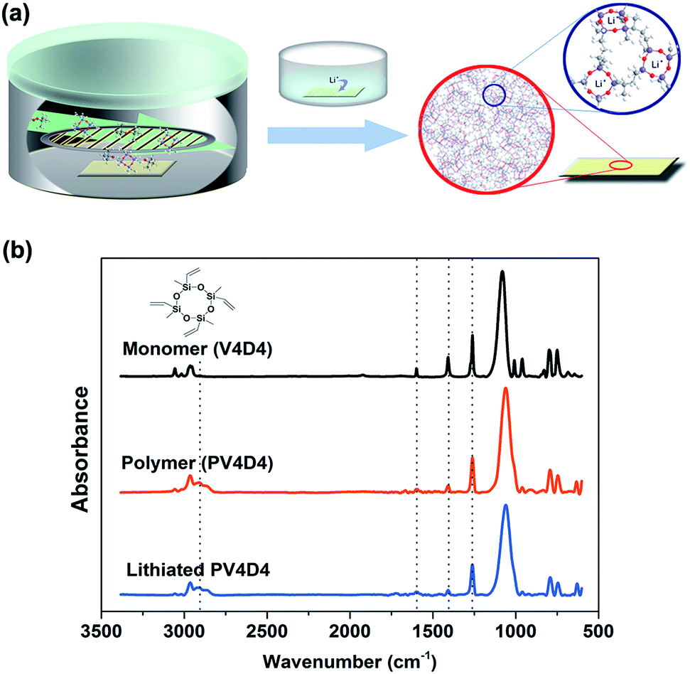 | ||
| Fig. 1 (a) Scheme for fabrication of PV4D4 electrolyte via iCVD and Li+ doping; (b) FTIR spectra of V4D4 monomer, PV4D4 and lithiated PV4D4, respectively. Inset depicts siloxane ring structure of V4D4 monomer. Vertical dash lines indicate changes between monomer and polymer spectra. Reduced peaks in polymer spectra around 1408 and 1600 cm−1 with unchanged peak at 1261 cm−1 confirm polymerization of the vinyl bond of the monomer. The strong absorption at 1060 cm−1 in all spectra indicates the Si–O–Si ring structures were retained after polymerization. Broader peaks around 2900 cm−1 in polymer spectra are due to absorptions from the polymer backbone, which is not observed in monomer spectrum. | ||
In order to verify the chemical structure of the deposited film, we measured FTIR of the monomer (V4D4), polymer (PV4D4) and the lithiated PV4D4. In Fig. 1b, strong peaks at 1060 cm−1 are due to Si–O vibrations from the retained Si–O–Si rings. Comparisons between polymer and monomer spectra confirm polymerization as the single-peak at 1261 cm−1 (Si–methyl) remains unchanged while peaks at 1408 cm−1 (CH2 deformation) and 1600 cm−1 (C![[double bond, length as m-dash]](https://www.rsc.org/images/entities/char_e001.gif) C) are reduced.5 Further evidence for the polymerization can be found around 2900 cm−1 indicating C–H stretching from the newly formed polyethylene-like backbone in the polymer. No obvious difference was observed between the spectra of original PV4D4 and the lithiated film. This is mainly because the major IR absorption of LiClO4 (Cl–O ν3 asymmetric stretching) appears around 1100 cm−1,30 which is overlapped by the strong Si–O absorption. The comparison also suggests the PV4D4 film remains chemically and mechanically intact without noticeable structural re-arrangement after the solution based lithiation step. We previously demonstrated that polysiloxane films are excellent electronic insulators that maintain high values of bulk electrical resistivity (>4 × 10¹⁵ Ω cm) under constant electrical bias for over 8 years.9 The highly cross-linked network from polymerization of multiple propagation (vinyl) sites is the main reason for the chemical and mechanical stability, which are attractive for electrolyte applications. In addition, such robust nanoscale conformal coatings can serve as protective layers on battery electrodes during electrochemical processes.31,32
C) are reduced.5 Further evidence for the polymerization can be found around 2900 cm−1 indicating C–H stretching from the newly formed polyethylene-like backbone in the polymer. No obvious difference was observed between the spectra of original PV4D4 and the lithiated film. This is mainly because the major IR absorption of LiClO4 (Cl–O ν3 asymmetric stretching) appears around 1100 cm−1,30 which is overlapped by the strong Si–O absorption. The comparison also suggests the PV4D4 film remains chemically and mechanically intact without noticeable structural re-arrangement after the solution based lithiation step. We previously demonstrated that polysiloxane films are excellent electronic insulators that maintain high values of bulk electrical resistivity (>4 × 10¹⁵ Ω cm) under constant electrical bias for over 8 years.9 The highly cross-linked network from polymerization of multiple propagation (vinyl) sites is the main reason for the chemical and mechanical stability, which are attractive for electrolyte applications. In addition, such robust nanoscale conformal coatings can serve as protective layers on battery electrodes during electrochemical processes.31,32
The morphology of iCVD PV4D4 films was characterized by TEM and AFM. Fig. 2a shows a TEM image of a bare Ag nanowire (160 nm in diameter). As shown in Fig. 2b, 10 nm PV4D4 film covers the nanowire uniformly, demonstrating excellent conformality of the film over high-aspect-ratio nanostructures thus maintaining the high surface area of the nanowire. Smoothness is also essential for thin-film electrolytes as large variations in thickness statistically increase the possibility of pinhole defects.14 AFM micrograph (Fig. S1 and S2†) depicts as-deposited PV4D4 film on silicon is extremely smooth with root mean square roughness (RRMS) of 0.46 nm. Fig. 2c shows that PV4D4 coated nanowires retain their morphology after lithiation with minimal change in film thickness (mean thickness and standard deviation over multiple nanowire samples is shown in Fig. S3†).
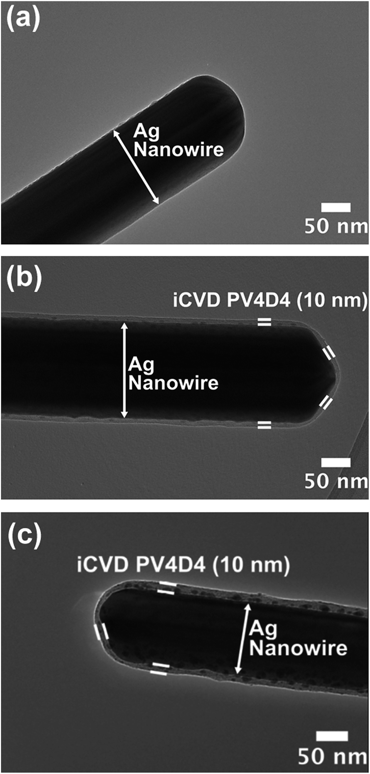 | ||
| Fig. 2 (a) TEM image of uncoated Ag nanowire; (b) 10 nm PV4D4 coated Ag nanowire; (c) 10 nm PV4D4 coated Ag nanowire after lithiation. | ||
Mechanical adhesion and chemical stability of these films were further verified by VASE measurements (Table S2 and Fig. S4†), which demonstrate no statistically significant change in thickness and refractive index of PV4D4 films after lithiation. Unlike typical polymer films which can swell ∼50%,29 the thickness change of PV4D4 films is minimal (<3%) after lithiation (Table S2†). Such minimal change in morphology and thickness of these nanoscale, conformal PV4D4 films upon lithiation is also attractive for deploying them as electrolytes in battery devices.
In Fig. 3, we demonstrate that the iCVD process used to engineer these nanoscale, conformal PV4D4 films can be uniformly scaled over a larger area. VASE measurements at various positions of a PV4D4 film grown on a 100 mm diameter silicon wafer show excellent uniformity – the standard deviation of measurements at different locations are within 4.6% of the average film thickness. These are encouraging results for commercialization of these electrolyte films, as the solvent-free iCVD polymerization process is readily scalable and easily integrated with other techniques, such as roll-to-roll processing.33
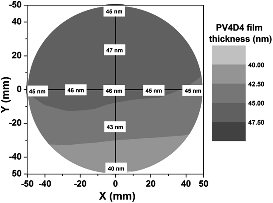 | ||
| Fig. 3 VASE measurements of iCVD PV4D4 films coated over a silicon wafer (100 mm in diameter). The standard deviation of the measurements at various locations are within 4.6% of the average film thickness. | ||
The electrical conductivities of unlithiated PV4D4 films were measured as 4.1 ± 2.4 × 10⁻¹¹ S cm−1 and 5.7 ± 3.4 × 10⁻¹¹ S cm−1 for the 25 and 35 nm films, respectively. The current–voltage plots (Fig. S5†) show an ohmic response and are stable over time. These measurements indicate that the unlithiated polymer films are excellent dielectrics and can withstand electric fields in excess of 104 V cm−1.
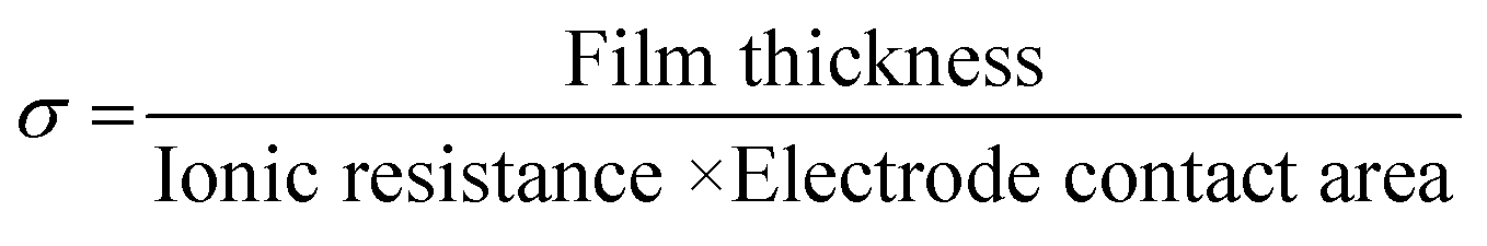
Impedance spectroscopy performed at multiple positions using a hanging Hg drop electrode arrangement (Fig. 4a) shows the dielectric response of the unlithiated 25 nm thick PV4D4 film as indicated by the vertical line in the Nyquist plot (Fig. 4b) and near −90° phase angles in the Bode plot over the entire range of frequencies (Fig. S6†). Similar results were measured on unlithiated 35 nm films. After lithiation, the impedance response of the PV4D4 film is that of an ionic conductor. The Nyquist plot for the lithiated 25 nm sample clearly depicts the characteristic semi-circles indicative of ionic transport (Fig. 4c). The impedance data for the 35 nm film (Fig. S7†) are also consistent with the RC circuit used to model charge transport. Using the averaged ionic resistance (Rp) determined from equivalent circuit fitting, the measured film thickness and the electrode contact area defined by Hg drop size, the ionic conductivity (σ) was calculated as follows:
 | (1) |
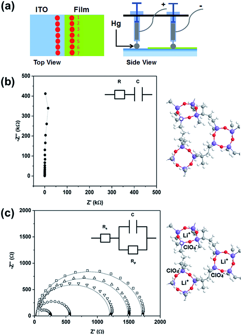 | ||
| Fig. 4 (a) Representation of the experimental configuration used for electrochemical impedance spectroscopy. Impedance of the (b) unlithiated and (c) lithiated 25 nm PV4D4 films. The data were taken in the frequency range from 100 kHz to 100 Hz using a 10 mV (RMS) potential. The circuits used for equivalent circuit fitting are shown. The semi-circles in (c) are indicative of ionic conduction. The solid curves were obtained from data fitting and used to determine Rp. Cartoon insets in (b) and (c) propose the PV4D4 structure before and after lithiation, respectively. Blue and red spheres represent Si and O atoms, respectively. In (b) and (c) the geometric markers indicate different positions on the sample. | ||
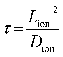
For the lithiated 25 nm PV4D4 film, σ is 7.5 ± 4.5 × 10⁻⁸ S cm−1 at room temperature. We hypothesize that oxygen atoms on siloxane rings of PV4D4 can provide favourable binding sites for Li+, while ClO4− counterions remain in the inter-ring space to minimize electrostatic repulsion (Fig. 4c). Besides Li+, ClO4− ions may also contribute to measured ionic conductivities. Efforts are currently ongoing to experimentally measure the Li+ transference number in order to determine the relative contributions of Li+ and ClO4− ions. The flexible Si–O–Si bonds further facilitate ion transport, resulting in ionic conduction at room temperature. For similar ionic diffusion coefficients (Dion), the ionic diffusion time (τ) increases as the square of the ionic diffusion length (Lion), as described by:27,34
 | (2) |
Accordingly, a 10 nm thick PV4D4 film exhibits 6 orders of magnitude lower ionic diffusion time (τ) compared to a 10 μm thick film of conventional electrolytes. Therefore, nanoscale electrolytes like PV4D4 can compensate for their modest ionic conductivity of ∼10−8 S cm−1 by their shorter ionic diffusion times, when compared with bulk electrolytes with higher conductivities. Additionally, as shown in Table S3,† iCVD synthesized PV4D4 films already demonstrate the highest ionic conductivity value reported among nanoscale, conformal thin film electrolytes. Furthermore, this value of conductivity at room temperature is important relative to that at higher temperature for several applications like sensing and medical implants that operate under ambient conditions.
For the thicker 35 nm PV4D4 film, σ = 1.3 ± 1.2 × 10⁻¹⁰ S cm−1. One hypothesis for the decrease in ionic conductivity as film thickness increases is that disorder in ring stacking increases with film thickness, leading to lower ionic conductivity. Alternatively, full lithiation of the thicker film may not have been achieved. While all positions on unlithiated PV4D4 film in Fig. 4a show dielectric behaviour, the variability in the impedance values seen at different positions on the lithiated PV4D4 film (Fig. 4c) suggests that there is an inhomogeneous distribution of charge carriers throughout the PV4D4 film. Optimization of the lithiation process is ongoing to eliminate this variability.
The absence of pinholes in a nanoscale thin film electrolyte is a critical issue for batteries in order to prevent short circuits caused by touching of anode and cathode particles. The most widely investigated thin film solid-state batteries typically have electrolyte thicknesses on the order of 1 μm and are sufficiently thick that pinholes are not problematic.35 However, in the present study, where the polymer films are on the order of 25 nm, the presence of pinholes is a greater concern. The approach we used to characterize pinholes in the PV4D4 films was based on electrochemical techniques which make use of different cyclic voltammetry signatures that depend on pinhole conditions in nanoporous, self-assembled monolayers.36,37 This method quantifies the number of pinholes of a given size over a specific area and thus provides a useful metric for evaluating an electrolyte as these defects represent potential currents paths that can lead to electrical shorting between electrodes.
The characterization method and the results obtained with the redox couples dmFc and CoCp2PF6 as probe molecules, are presented in Fig. S8 and S9.† Based on the cyclic voltammetry results, the pinholes can be reasonably estimated to be in the same size regime as the probe molecules, or approximately 4 nm in diameter.37 The number density of these pinholes were calculated (Table 1) and found to be somewhat less than those reported for self-assembled monolayers based on organomercaptans,37 suggesting that these PV4D4 films are effectively pinhole free. Moreover, the number density of pinholes decreases upon lithiation. This effect is most likely due to the closing of some pinholes as a result of the expansion of the PV4D4 film from the incorporation of LiClO4, as demonstrated by a slight increase in film thickness after lithiation (Table S2†).
| PV4D4 film | Redox couple | Peak current density [μA cm−2] | Number density of pinholes [pinholes μm−2] |
|---|---|---|---|
| Unlithiated 20 nm | dmFc | 23.50 | 8.01 |
| Unlithiated 20 nm | CoCp2PF6 | 14.00 | 3.68 |
| Lithiated 20 nm | dmFc | 14.50 | 4.94 |
| Lithiated 20 nm | CoCp2PF6 | 9.35 | 2.46 |
Conclusions
In this work, we have addressed a key material limitation which has prevented the realization of high energy density compact power systems with 3D architectures, namely the lack of a nanoscale thin film electrolyte to conformally coat non-planar electrode arrays. We demonstrate that electrically insulating nanoscale PV4D4 thin films with a built-in ring structure can conduct ions and that these films can be conformal on high-aspect-ratio nanowires. The polysiloxane films synthesized by iCVD show minimal change in morphology and thickness change during lithiation, in addition to being smooth and pinhole free. The short diffusion lengths in these nanoscale films compensate for their modest ionic conductivities by providing orders of magnitude lower ionic diffusion times in comparison to bulk or microscale polymeric electrolytes. Being the workhorse technology for growing inorganic thin films in the microelectronics industry, CVD is a proven and cost-effective technology, which when coupled with the flexibility of organic chemistry can engineer novel nanoscale thin film electrolytes for the emerging field of 3D batteries.Acknowledgements
The authors acknowledge the support from the Office of Naval Research under funding Contract N00014-13-1-0466.Notes and references
- D. R. Rolison, J. W. Long, J. C. Lytle, A. E. Fischer, C. P. Rhodes, T. M. McEvoy, M. E. Bourg and A. M. Lubers, Chem. Soc. Rev., 2009, 38, 226–252 RSC.
- T. S. Arthur, D. J. Bates, N. Cirigliano, D. C. Johnson, P. Malati, J. M. Mosby, E. Perre, M. T. Rawls, A. L. Prieto and B. Dunn, MRS Bull., 2011, 36, 523–531 CrossRef CAS.
- J. W. Long, B. Dunn, D. R. Rolison and H. S. White, Chem. Rev., 2004, 104, 4463–4492 CrossRef CAS.
- A. M. Coclite, R. M. Howden, D. C. Borrelli, C. D. Petruczok, R. Yang, J. L. Yagüe, A. Ugur, N. Chen, S. Lee, W. J. Jo, A. Liu, X. Wang and K. K. Gleason, Adv. Mater., 2013, 25, 5392–5423 CrossRef CAS PubMed.
- W. S. O'Shaughnessy, M. L. Gao and K. K. Gleason, Langmuir, 2006, 22, 7021–7026 CrossRef PubMed.
- N. J. Trujillo, Q. G. Wu and K. K. Gleason, Adv. Funct. Mater., 2010, 20, 607–616 CrossRef CAS.
- K. K. S. Lau and K. K. Gleason, Macromolecules, 2006, 39, 3688–3694 CrossRef CAS.
- K. K. S. Lau and K. K. Gleason, Macromolecules, 2006, 39, 3695–3703 CrossRef CAS.
- W. S. O'Shaughnessy, S. K. Murthy, D. J. Edell and K. K. Gleason, Biomacromolecules, 2007, 8, 2564–2570 CrossRef PubMed.
- H. Jung, M. Kim, Y. Kim, S. Oh, C.-J. Kang, T.-S. Yoon and H. H. Lee, Microelectron. Eng., 2014, 118, 6–10 CrossRef CAS PubMed.
- A. L. M. Reddy, S. R. Gowda, M. M. Shaijumon and P. M. Ajayan, Adv. Mater., 2012, 24, 5045–5064 CrossRef CAS PubMed.
- D. E. Fenton, J. M. Parker and P. V. Wright, Polymer, 1973, 14, 589 CrossRef CAS.
- C. Berthier, W. Gorecki, M. Minier, M. B. Armand, J. M. Chabagno and P. Rigaud, Solid State Ionics, 1983, 11, 91–95 CrossRef CAS.
- F. Croce, G. B. Appetecchi, L. Persi and B. Scrosati, Nature, 1998, 394, 456–458 CrossRef CAS PubMed.
- D. T. Hallinan and N. P. Balsara, Annu. Rev. Mater. Res., 2013, 43, 503–525 CrossRef CAS.
- G. B. Zhou, I. M. Khan and J. Smid, Macromolecules, 1993, 26, 2202–2208 CrossRef CAS.
- D. P. Siska and D. F. Shriver, Chem. Mater., 2001, 13, 4698–4700 CrossRef CAS.
- Z. Zhang, L. J. Lyons, J. J. Jin, K. Amine and R. West, Chem. Mater., 2005, 17, 5646–5650 CrossRef CAS.
- N. A. A. Rossi and R. West, Polym. Int., 2009, 58, 267–272 CrossRef CAS.
- M. Burjanadze, Y. Karatas, N. Kaskhedikar, L. M. Kogel, S. Kloss, A.-C. Gentschev, M. M. Hiller, R. A. Müller, R. Stolina, P. Vettikuzha and H.-D. Wiemhöfer, Z. Phys. Chem., 2010, 224, 1439–1473 CrossRef CAS.
- X. Chen, M. Usrey, A. Peña-Hueso, R. West and R. J. Hamers, J. Power Sources, 2013, 241, 311–319 CrossRef CAS PubMed.
- X. Hu, M. D. Tang-Schomer, W. W. Huang, X. X. Xia, A. S. Weiss and D. L. Kaplan, Adv. Funct. Mater., 2013, 23, 3875–3884 CrossRef CAS PubMed.
- H. Hu, W. Yuan, H. Zhao and G. L. Baker, J. Polym. Sci., Part A: Polym. Chem., 2014, 52, 121–127 CrossRef CAS.
- Z. Jia, W. Yuan, H. Zhao, H. Hu and G. L. Baker, RSC Adv., 2014, 4, 41087–41098 RSC.
- A. S. Arico, P. Bruce, B. Scrosati, J. M. Tarascon and W. Van Schalkwijk, Nat. Mater., 2005, 4, 366–377 CrossRef CAS PubMed.
- P. W. Zheng and T. J. McCarthy, Langmuir, 2010, 26, 18585–18590 CrossRef CAS PubMed.
- K. Zhang, X. Han, Z. Hu, X. Zhang, Z. Tao and J. Chen, Chem. Soc. Rev., 2015 10.1039/c4cs00218k.
- C. D. Petruczok, N. Chen and K. K. Gleason, Langmuir, 2014, 30, 4830–4837 CrossRef CAS PubMed.
- C. P. Rhodes, J. W. Long, M. S. Doescher, J. J. Fontanella and D. R. Rolison, J. Phys. Chem. B, 2004, 108, 13079–13087 CrossRef CAS.
- Y. Chen, Y. H. Zhang and L. J. Zhao, Phys. Chem. Chem. Phys., 2004, 6, 537–542 RSC.
- Y. S. Jung, A. S. Cavanagh, L. A. Riley, S. H. Kang, A. C. Dillon, M. D. Groner, S. M. George and S. H. Lee, Adv. Mater., 2010, 22, 2172–2176 CrossRef CAS PubMed.
- L. A. Riley, A. S. Cavanagh, S. M. George, Y. S. Jung, Y. F. Yan, S. H. Lee and A. C. Dillon, Chemphyschem, 2010, 11, 2124–2130 CrossRef CAS PubMed.
- M. Gupta and K. K. Gleason, Thin Solid Films, 2006, 515, 1579–1584 CrossRef CAS PubMed.
- M. Park, Z. Xhang, M. Chung, G. B. Less and A. M. Sastry, J. Power Sources, 2010, 195, 7904–7929 CrossRef CAS PubMed.
- N. Dudney, Interface, 2008, 17, 44–48 CAS.
- O. Chailapakul and R. M. Crooks, Langmuir, 1993, 9, 884–888 CrossRef CAS.
- O. Chailapakul and R. M. Crooks, Langmuir, 1995, 11, 1329–1340 CrossRef CAS.
Footnotes |
| † Electronic supplementary information (ESI) available: iCVD synthesis details, AFM images, VASE data, comparison of thin film electrolytes, pinhole characterization. See DOI: 10.1039/c4mh00246f |
| ‡ These authors contribute equally. |
| This journal is © The Royal Society of Chemistry 2015 |