
Higher mobility in bulk semiconductors by separating the dopants from the charge-conducting band – a case study of thermoelectric PbSe
Heng
Wang
*ae,
Xianlong
Cao
b,
Yoshiki
Takagiwa
c and
G. Jeffrey
Snyder
*ade
aMaterials Science, California Institute of Technology, Pasadena, CA 91125, USA. E-mail: hengwang@caltech.edu; jsnyder@caltech.edu
bDepartment of Metallurgy and Materials Engineering, Chongqing University of Science and Technology, Chongqing 401331, China
cDepartment of Advanced Materials Science, The University of Tokyo, Kiban-toh 502, 5-1-5 Kashiwanoha, Kashiwa-shi, Chiba 277-8561, Japan
dITMO University, Saint Petersburg, Russia
eMaterials Science and Engineering, Northwestern University, Evanston, Il 60208, USA
First published on 10th March 2015
Abstract
In the rigid band approximation dopants in semiconductors only change the Fermi level and carrier concentration such that different dopants are thought equivalent when fully ionized. In this work we examine the small but significant difference in mobility due to the type of dopant in heavily doped PbSe by studying n-type samples doped with Br, In and Bi. We propose that cation and anion dopants lead to a difference in mobility at high concentrations. This can be understood considering the predominance of cation states to the conduction band and anion states to the valence band. For higher mobility and better performance for most applications of heavily doped semiconductors, dopants should be on the site that is of less influence on the charge-conducting band. This concept can be viewed as an analog of modulation doping on the atomic level. Its physical origin is the random potential due to disorder that perturbs carriers, which is also the origin of Anderson localization at low temperature, a well-studied topic in theoretical physics. In thermoelectric PbSe, the selection of dopant can lead to 10% difference in mobility and in zT.
Conceptual insightsA major effort in semiconductor, and in particular thermoelectrics, is to achieve an optimum carrier concentration through doping so the material performance is maximized. In the rigid band approach, different dopants are considered equivalent if they could produce the same level of doping. In this work we show that although this is true on the first order, the choice of dopant does make a difference in the carrier mobility of heavily doped semiconductors. Higher mobilities on average are found in samples with dopants on the sub-lattice that made less contribution to the formation of the charge-conducting band. This advances our understanding of the general problem of doping such that in addition to proper carrier concentration tuning, it further requires a rational choice of dopant to realize the best material properties. The guidelines presented here can be applied to various applications of heavily doped semiconductors for more efficient material optimization. |
Introduction
For most of their applications semiconductors need to be doped to have desired electrical properties. In many cases this is done by substituting some of the atoms with a different element e.g., the dopant. Adjusting the dopant content, and hence free carrier concentration, provides essential control over conductivity for each specific application.Doping of a semiconductor also affects the transport properties through carrier scattering events as the existence of impurities inevitably gives rise to additional carrier scattering. Classic transport theory formulates the interaction between carriers and dopant impurities with a columbic interaction between charge carriers and the ionized atomic core: the ionized impurity scattering.1 The formulism does not take into account details of the impurity other than its relative valence such that different dopants with the same valence are considered equivalent as long as they are fully ionized without compensation (we shall exclude special cases where the dopants are of resonant nature2–4).
A majority of applications of semiconductors in electronic, optoelectronic, or photovoltaic devices use dilute doping with free carrier density below 1018 cm−3 (about 0.01% atomic substitution for monovalent dopant), where the different nature of dopants is described by the discrete defect levels observable at low concentrations and low temperatures. Once the carriers are activated their mobility is thought determined by the host material rather than the type of dopant. Some applications such as thermoelectric materials,5,6 or conductive oxides7,8 require doping of semiconductors to carrier densities between 1019 and 1021 cm−3, corresponding to dopant concentrations of up to a few percent, heavily doped semiconductors show metallic behavior and the activation of carriers are not observed.9
In this work we compare the influence of different dopants on mobility in heavily doped compound semiconductors. The compound studied here is PbSe, which has received great interest10–13 recently as a promising thermoelectric material for application between 600 K and 900 K. We find that for free electron density above 2 × 1019 cm−3, the anion dopants lead to higher mobility than the cation dopants. This can be qualitatively understood with a picture14 given by Ioffe (Fig. 1): the same degree of disorder leads to less mobility reduction when it is introduced on the sub-lattice that has less character for the charge conducting band. Also note that heavily doped semiconductors are essentially disordered systems, hence the underlying physics shares the same origin with other known effects associated with disorder, for instance, the Anderson localization,15,16 which has been extensively studied in theoretical physics. Separating the disorder of doping from the part of the crystal most relevant to the charge transport enables higher mobilities. We further demonstrate that the difference in mobility found in PbSe is also seen in other heavily doped compound semiconductors. Thus we conclude that there is a chemical effect from the dopants for heavily doped compound semiconductors, which leads to a difference in carrier mobility for the same amount of dopant.
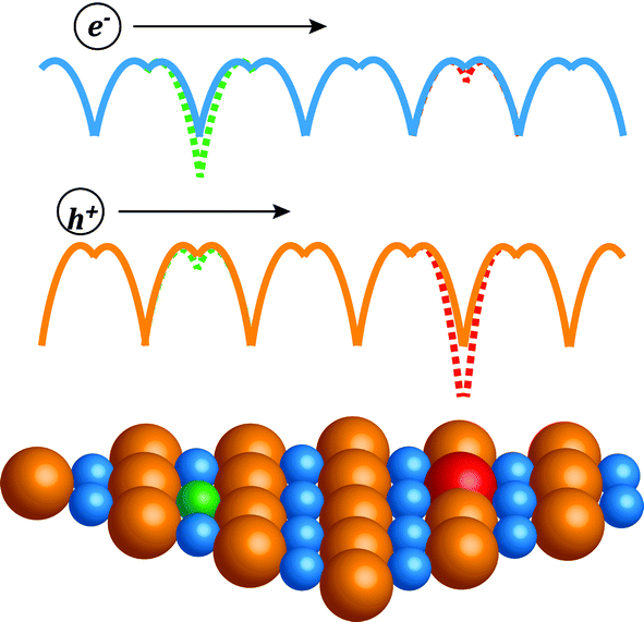 | ||
| Fig. 1 In an ionic lattice the conduction band is mostly formed by cation (blue) atomic orbitals and the valence band by anion (orange) orbitals, hence a donor on the cation site (green) causes a larger perturbation of the periodic potential (illustrated as colored lines) to the conduction band, which scatters electrons more than holes; whereas a donor on the anion site (red) perturbs more the valence band and therefore the holes. | ||
A well-known principle of doping for higher mobility is the modulation doping in heterostructures,17,18 where the dopants are spatially separated from the two-dimensional electron gas formed at an interface. In nanostructured bulk semiconductors, it has also been suggested19,20 that a modulated doping profile leads to higher conductivity. The difference in mobility seen here is the result of an effect analogous to the modulation doping on the atomic level.
Experimental methods
All samples are made with melting and reacting the elements followed by annealing and consolidation. The experimental detail for Br doped PbSe with slight Pb excess (Pb1.002Se1−xBrx) was reported previously.21 For the cation substituted samples elements were weighed according to formula Pb1.002−xInxSe and Pb1−xBixSe, then sealed in carbon coated quartz ampoules with vacuum <10−4 torr and melted at 1373 K for 6 hours, followed by water quenching. The ingots were annealed in the same ampoule at 950 K for 3 days. Hand ground ingots were then consolidated with induction heated hot press22 at 873 K under 1 atm argon and uniaxial pressure of 40 MPa for 20 minutes. All samples are dense with >98% relative density. These samples have nearly ideal doping efficiency from charge counting assuming one carrier for each dopant atom. The temperature dependent resistivity and Hall coefficient were measured by the van der Pauw method.23 The Seebeck coefficient at different temperatures was measured under oscillating temperatures with Chromel–Nb thermocouples.24 These properties are isotropic based on previous study on Br doped PbSe. For each measurement data were collected during both heating and cooling. The uncertainty of each measurement is about 5%.Density of states calculation was performed using the Korringa–Kohn–Rostoker Green function formalism under the coherent potential approximation (KKR-CPA). The experimental room-temperature lattice constants and the von Barth–Hedin formula25 for the exchange energy were used. For all atoms the angular momentum cut-off, lmax = 2 was set and semi-relativistic calculations of core level were employed. A dense mesh of 600 k points in the irreducible wedge of the Brillouin-zone was used. Final converged total energy below 10−6 Ry was applied in the self-consistent cycle. The energy at valence band edge is set as zero.
For bulk materials the influence from compensating defects or grain boundary trapping of dopants could easily affect the observed influence of the dopants. We try to mitigate this in multiple ways. First, lead chalcogenides have extraordinarily large dielectric constants26 which screen the long-range effects from structural defects, making it possible to achieve mobilities in polycrystalline samples as high as in single crystals and high quality thin films. Second, we compare multiple batches and use only samples with no compensation/activation behavior for analysis. The doping efficiency is close to 100% for all samples from this study shown. One measure to achieve this is by using a slight excess of Pb to prevent “killer” Pb vacancy defects27 (not for Bi doping due to its amphoteric nature); third, we compare our result with all literature values and assure they reflect the highest mobilities achieved.
Results and discussion
Comparing different n-type dopants (Fig. 2) we find that higher mobility is achieved with anion dopants as opposed to cation dopants. Fig. 2(a), which shows the mobilities of cation and anion doped n-type PbSe at 300 K, includes results from our studies as well as other results for n-type PbSe (only the high mobility samples are compared). Halogens are common dopants on the anion site for lead chalcogenides and we have used Br for our previous study21 on n-type PbSe due to its closest atomic size to Se, whereas Cl is also often used by other researchers.28–30 Interestingly the use of Cl leads to the same mobilities as Br (for same nH) despite of the atomic size difference. Typical cation dopants for lead chalcogenides include group III elements Al, Ga, In and group V elements Sb, Bi. In this work we made In and Bi doped PbSe because the atomic sizes are closest to Pb. Doping by other group III (ref. 31–34) and group V (ref. 35) elements has been reported by other researchers and most of these results are also included. Rare-earth elements have also been used for PbTe36,37 or PbSe,38,39 we found in PbSe their doping efficiency is very low39 (about 5% from charge counting for La) thus the results are not included. Doping of PbSe with transition metal Nb has also been reported40 where the study found a significant change of effective mass, presumably due to change in band structure, so this result is not compared.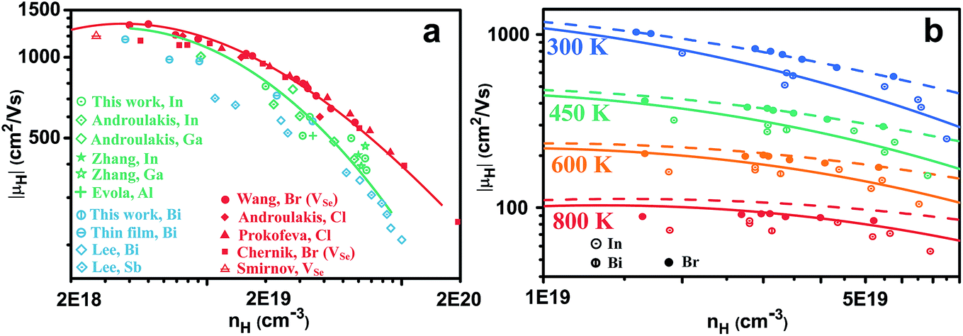 | ||
| Fig. 2 (a) Hall mobilities of n-type PbSe as a function of carrier density at 300 K. The red curve is calculated for deformation potential phonon scattering only, the green curve is that plus disorder scattering. (b) Hall mobilities at different temperatures. The solid and dashed curves are calculated the same way as the red and the green curve in (a), respectively. | ||
For samples with nH = 2 × 1019 cm−3 and above, there is a striking difference between cation and anion doped samples, throughout all studies from different groups. High mobility is achieved only from anion doped samples, cation dopants are distinctly inferior. Moreover, the difference in mobility between cation and anion doped PbSe remains at high temperatures as shown in Fig. 2(b).
A lower mobility could come from either a heavier effective mass or increased carrier scattering, the former one is less likely as the effective mass appears unchanged. The same density of states effective mass is demonstrated by the similar carrier density dependence of the Seebeck coefficient, as shown in Fig. 3 for both (a) 300 K and (b) different temperatures. Keeping in mind the uncertainty in both carrier density and Seebeck coefficient measurements, which can be expected to be less within the same research groups, Fig. 3(a) suggests that the effective mass does not change (at least not significantly) with different types of dopants (for example, compare the results from Androulakis et al. on both Cl and In, Ga; or results from Wang et al. on Br and this work). Historically In was suggested30 to be a resonant dopant in PbSe below or at 300 K, however the transport properties from our study suggests only regular doping behavior at 300 K and above. We notice that this agrees with recent independent reports by Androulakis et al.34 and Evola et al.31 As the temperature increases, again the same Pisarenko relation is seen for anion (Br) and cation (In, Bi) doped samples, as shown in Fig. 3(b).
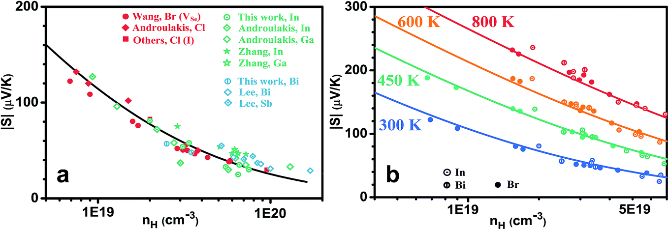 | ||
| Fig. 3 (a) Pisarenko plot of thermopower (absolute value of Seebeck Coefficient) at 300 K. Different dopants do not change the effective mass of carriers to the first order. (b) Pisarenko plot at different temperatures. | ||
The electronic density-of-states (DOS) of PbSe upon 0.3% doping with Br, Bi and In are calculated using the Korringa–Kohn–Rostoker Green function formalism under the coherent potential approximation (KKR-CPA), as shown in Fig. 4. For Bi, the DOS near the band gap stays identical to undoped PbSe, which validates the rigid band assumption41 commonly used in doping-related modeling. For In additional states are seen near the conduction band edge. These states are In s-states that may be localized. Although at lower temperatures they might lead to anomaly in transport that gives this dopant its resonant behavior, at room temperature and above they showed experimentally no change to the effective mass of the charge carriers. Note that the local lattice relaxation due to In substitution is not accounted for in the KKR-CPA calculation, so the DOS distortion shown could also be an artifact of the calculation. The anion dopant Br, is found to best maintain the host DOS up to deep inside the conduction band. This is still true even for the case of 3% substitution, where Br still complies with the rigid band assumption. Both In and Bi at this level on the other hand, alter the host band structure noticeably.
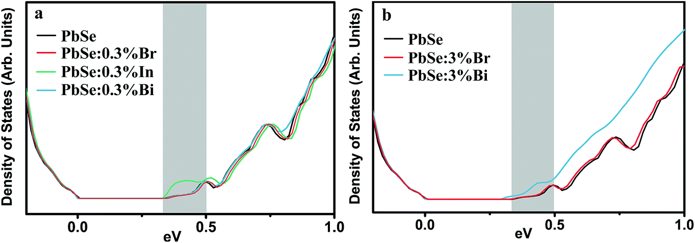 | ||
| Fig. 4 Calculated density of states for PbSe doped with (a) 0.3% and (b) 3% of substitutional impurities. Shaded region marks the part of conduction band relevant to the room temperature transport in heavily doped n-type, thermoelectric PbSe. | ||
The speed of sound at 300 K are measured for PbSe with 0.3% substitutional Br, Bi and In, no difference beyond the uncertainty of the measurement were seen, indicating the elastic properties of PbSe are not affected by small amount of dopants. Thus all the material parameters21 that determine the magnitude of acoustic phonon scattering: effective mass m*b, average longitudinal elastic modulus Cl, and deformation potential coefficient Ξ, remained unchanged (the inherent material property Ξ should not be affected by impurities on such level).
Impurities introduce perturbation to the potential energy felt by the electronic states. Although the most considered perturbation for dopant impurities derives from the long-range, columbic potential that results in the ionized impurity scattering,1,42 this mechanism does not dominate the mobility difference seen in this study. For one, the ionized impurity scattering theory treats different dopants equivalently (for example the Brooks and Herring formula) as long as they are of the same valence, fully ionized and randomly distributed. But more importantly, the large dielectric constants in Pb chalcogenides screens the columbic perturbation from ionized impurities such that it is only an insignificant fraction of the total scattering observed.
The short-range interaction remains in this case. It can be described in the same way as the potential perturbation from isovalent substitution. For mobility reduction caused by isovalent substitution, Ioffe made a very simple argument14 comparing n- and p-type PbTe1−xSex: since the conduction band is has stronger cation character than anion character of atomic electronic states, the substitution on the anion site would disturb the valence band more than the conduction band. Thus the mobility reduction in p-type PbTe1−xSex was found43 greater than n-type. Ioffe's argument depicts the same physical picture that leads to the Anderson localization, which describes a metal to insulator transition at low temperatures when the random potential due to disorder makes the otherwise extended states localized. At temperatures or carrier energies high enough to prevent localization, the random potential manifests itself as an Anderson localization driven mobility reduction. For the isovalent substitutional case this is well known as the disorder scattering.44,45 The similar effect from dopant impurities is much less considered for the carrier scattering process. Nonetheless some researchers have included it as an additional correction term in potential energy as either a “central cell46” correction or “strain47” induced effect, which reduced the discrepancy between ionized impurity scattering theory and experimental mobilities.
Analogous to disorder scattering, we write the relaxation time for the short-range potential scattering due to dopants in a similar format for nonparabolic, Kane type bands:
 | (1) |
Two reasons may explain why the short-range potential scattering from dopants is not normally essential to model the mobility. First its localized nature makes it insignificant for lightly doped semiconductors; second, its carrier energy and temperature dependence is too similar to the deformation potential phonon scattering, making them difficult to accurately distinguish from experimental data. Nonetheless, as a semiconductor becomes more heavily doped one can expect the short-range potential scattering effect from dopants to become important. Moreover, in contrast to the mobility due to ionized impurity scattering that shows weak temperature dependence,7 the mobility from short-range potential scattering decreases with temperature, suggesting its increasing importance for higher temperatures whereas ionized impurity scattering is usually observed at lower temperatures.
Besides the mobility, PbSe doped with anion impurities are found with much better reproducibility when made multiple times, and enables more precise control of the carrier density. This is also reflected in literature data where for the anion doped PbSe the doping efficiency is usually close to 100% and the mobilities are in good agreement, whereas for cation doped PbSe low doping efficiency is often seen,51 and the mobilities are much more scattered.31,33 As a possible reason of this, Zunger's doping principle27 for compound semiconductors points out that cation doping for n-type semiconductors is less favorable because: effective cation site doping requires cation-rich host compound to suppress the formation of defects (either cation vacancy or anion interstitial) that compensates free electrons; at the same time the host needs to be kept cation-poor to ensure good solubility of cation site impurities. The present study further suggests that even if one managed to achieve efficient cation doping in a n-type semiconductor the mobility is very likely to be not as high as the anion doped counterpart.
PbSe is a promising thermoelectric material and previous studies12,13,35,52 have suggested zT > 1 in both n- and p-type at 850 K. Fig. 5 plots zT for n-type PbSe doped with anion and cation dopants. The curves are calculated based on material parameters determined previously53 and through the current study. A net free electron density of 3.3 × 1019 cm−3 was chosen to produce optimized zT around 850 K, which is in consistent with experimentally observed values.21,29,33 To the first order high zT could be achieved with either anion or cation dopants. However, because of the demonstrated difference in mobilities, samples with anion dopants on average should produce zT 10% higher than those with cation dopants, even though the uncertainty in measurements and variation among samples could easily overshadow such difference.
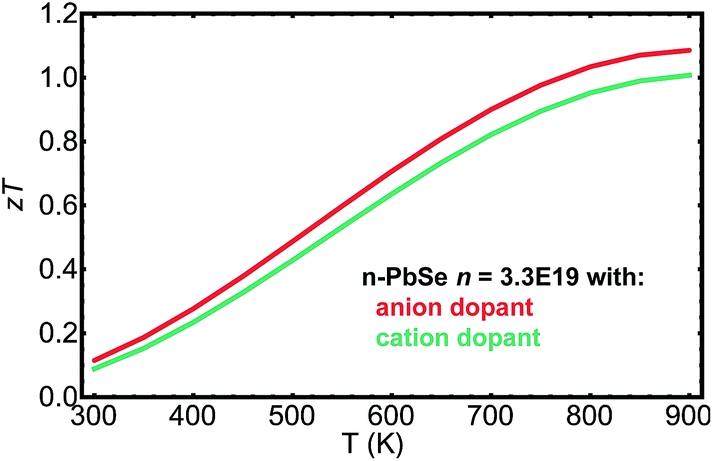 | ||
| Fig. 5 zT calculated as function of temperature for n type PbSe with carrier density 3.3 × 1019 cm−3, doped with anion dopants and cation dopants. | ||
In a broader context, we would like to demonstrate with two examples here that the trend seen in PbSe is also seen in other semiconductors that can be doped beyond 1019 cm−3 with dopants on different lattice sites. The first is n-type PbTe (Fig. 6a), samples doped with anion dopant iodine (ref. 54, and reference thereafter) have higher mobilities compared with most reported values using cation dopants55–59 (some samples from studies60,61 by Jaworski et al. indicate mobilities comparable with I doped ones). The second example is the III–V semiconductor of GaAs, GaAs can be doped heavily p-type with either Zn, Be on the cation site62–65 or Ge, Sn on the anion site,66,67 those with cation dopants in this case show higher mobilities. Even though GaAs is generally considered a covalent compound, its valence band has more contribution68 from As states, this aligns again with Ioffe's picture illustrated in Fig. 1.
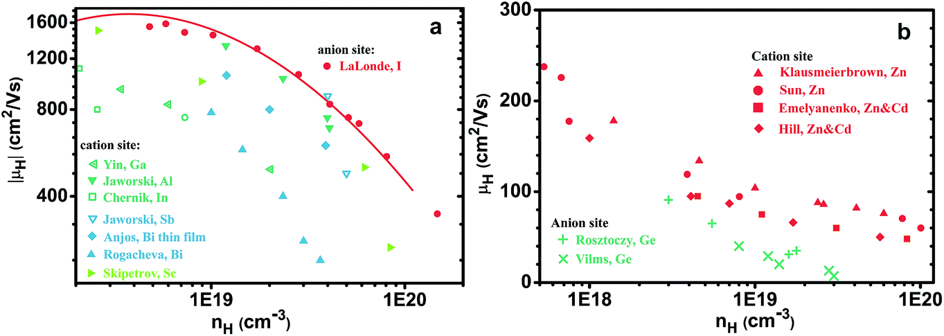 | ||
| Fig. 6 Mobilities at 300 K as functions of carrier density for (a) n-type PbTe and (b) p-type GaAs, both doped with dopants on different site. Anion dopants lead to higher mobility for electrons and cation dopants lead to higher mobility for holes. | ||
As a supplementary remark, it is worth pointing out that dopants should not be considered equivalent for heavily doped semiconductors in general. Even for the covalent, elemental semiconductor of Si, it is known69 that P doped Si has higher mobility than those doped with As once carrier density is above 1019 cm−3. Selberherr et al. explained this as a correction to the ionized impurity scattering theory using a carrier wave-vector dependent “effective charge” that differs among dopant species.70 For Pb chalcogenides ionized impurity scattering has insignificant influence, which is consistent with the finding here that different dopant species on the same lattice site led to similar mobilities. Nonetheless, in general dopants could be different even when they substitute the same site for a semiconductor with small static dielectric constant.
Conclusion
In summary, for heavily doped compound semiconductors dopants on different sites could make a difference on the mobility of carriers. We explain such difference found in PbSe with the difference in magnitude of disorder scattering from dopants. When heavily doping a compound semiconductor it is preferable to have the dopant on the lattice site with less influence on the charge-conducting band. Choosing the right type of dopant can be indispensable to optimizing the electronic performance of semiconductors.Acknowledgements
This work was supported as part of the Solid-State Solar-Thermal Energy Conversion Center (S3TEC), an Energy Frontier Research Center funded by the U.S. Department of Energy, Office of Science, Basic Energy Sciences under Award # DE-SC0001299. X. C. acknowledges support from Scientific and Technological Research Program of Chongqing Municipal Education Commission (KJ1401314 & KJ1401310); Cooperative Project of Academician Workstation of Chongqing U. Sci. & Tech. (CKYS2014Z03); Research Foundation of Chongqing U. Sci. & Tech. (CK2014Z22). Y. I. acknowledges support from JSPS KAKENHI Grant No. 26709051. The authors would like to thank Prof. Gang Chen and Prof. David Singh for insightful comments.References
- D. Chattopadhyay and H. J. Queisser, Rev. Mod. Phys., 1981, 53, 745–768 CrossRef CAS.
- V. I. Kaidanov, S. A. Nemov and Y. I. Ravich, Sov. Phys. Semiconduct., 1992, 26, 113–125 Search PubMed.
- J. P. Heremans, V. Jovovic, E. S. Toberer, A. Saramat, K. Kurosaki, A. Charoenphakdee, S. Yamanaka and G. J. Snyder, Science, 2008, 321, 554–557 CrossRef CAS PubMed.
- J. P. Heremans, B. Wiendlocha and A. M. Chamoire, Energy Environ. Sci., 2012, 5, 5510–5530 CAS.
- L. E. Bell, Science, 2008, 321, 1457–1461 CrossRef CAS PubMed.
- G. J. Snyder and E. S. Toberer, Nat. Mater., 2008, 7, 105–114 CrossRef CAS PubMed.
- K. Ellmer, Nat. Photonics, 2012, 6, 809–817 CrossRef CAS.
- T. Minami, Semicond. Sci. Technol., 2005, 20, S35 CrossRef CAS.
- M. N. Alexander and D. F. Holcomb, Rev. Mod. Phys., 1968, 40, 815–829 CrossRef CAS.
- D. Parker and D. J. Singh, Phys. Rev. B: Condens. Matter Mater. Phys., 2010, 82, 035204 CrossRef.
- H. Wang, Y. Pei, A. D. Lalonde and G. J. Snyder, Adv. Mater., 2011, 23, 1366–1370 CrossRef CAS PubMed.
- L. D. Zhao, S. Hao, S. H. Lo, C. I. Wu, X. Zhou, Y. Lee, H. Li, K. Biswas, T. P. Hogan, C. Uher, C. Wolverton, V. P. Dravid and M. G. Kanatzidis, J. Am. Chem. Soc., 2013, 135, 7364–7370 CrossRef CAS PubMed.
- H. Wang, Z. M. Gibbs, Y. Takagiwa and G. J. Snyder, Energy Environ. Sci., 2014, 7, 804 CAS.
- Y. I. Ravich, in Lead Chalcogenides Physics and Applications, ed. D. Khokhlov, Taylor & Francis, New York, 2003, vol. 18 Search PubMed.
- A. Lagendijk, B. van Tiggelen and D. S. Wiersma, Phys. Today, 2009, 62, 24–29 CrossRef CAS PubMed.
- B. Kramer and A. MacKinnon, Rep. Prog. Phys., 1993, 56, 1469 CrossRef CAS.
- L. Pfeiffer, K. W. West, H. L. Stormer and K. W. Baldwin, Appl. Phys. Lett., 1989, 55, 1888 CrossRef CAS PubMed.
- R. Gaska, M. S. Shur, A. D. Bykhovski, A. O. Orlov and G. L. Snider, Appl. Phys. Lett., 1999, 74, 287 CrossRef CAS PubMed.
- M. Zebarjadi, G. Joshi, G. H. Zhu, B. Yu, A. Minnich, Y. C. Lan, X. W. Wang, M. Dresselhaus, Z. F. Ren and G. Chen, Nano Lett., 2011, 11, 2225–2230 CrossRef CAS PubMed.
- B. Yu, M. Zebarjadi, H. Wang, K. Lukas, D. Wang, C. Opeil, M. Dresselhaus, G. Chen and Z. Ren, Nano Lett., 2012, 12, 2077–2082 CrossRef CAS PubMed.
- H. Wang, Y. Pei, A. D. LaLonde and G. J. Snyder, Proc. Natl. Acad. Sci. U. S. A., 2012, 109, 9705–9709 CrossRef CAS PubMed.
- A. D. LaLonde, T. Ikeda and G. J. Snyder, Rev. Sci. Instrum., 2011, 82, 025104 CrossRef PubMed.
- K. A. Borup, E. S. Toberer, L. D. Zoltan, G. Nakatsukasa, M. Errico, J. P. Fleurial, B. B. Iversen and G. J. Snyder, Rev. Sci. Instrum., 2012, 83, 123902 CrossRef PubMed.
- S. Iwanaga, E. S. Toberer, A. Lalonde and G. J. Snyder, Rev. Sci. Instrum., 2011, 82, 063905 CrossRef PubMed.
- U. V. Barth and L. Hedin, J. Phys. C: Solid State Phys., 1972, 5, 1629 CrossRef.
- E. G. Bylander and M. Hass, Solid State Commun., 1966, 4, 51–53 CrossRef CAS.
- A. Zunger, Appl. Phys. Lett., 2003, 83, 57–59 CrossRef CAS PubMed.
- I. A. Chernik, V. I. Kaidanov and E. P. Ishutinov, Sov. Phys. Semiconduct., 1969, 2, 825–829 Search PubMed.
- J. Androulakis, D. Y. Chung, X. L. Su, L. Zhang, C. Uher, T. C. Hasapis, E. Hatzikraniotis, K. M. Paraskevopoulos and M. G. Kanatzidis, Phys. Rev. B: Condens. Matter Mater. Phys., 2011, 84, 155207 CrossRef.
- L. V. Prokofeva, E. A. Gurieva, S. M. Zhumaksanov, P. P. Konstantinov, K. R. Mailina, Y. I. Ravich and L. S. Stilbans, Sov. Phys. Semiconduct., 1987, 21, 1078–1080 Search PubMed.
- E. G. Evola, M. D. Nielsen, C. M. Jaworski, H. Jin and J. P. Heremans, J. Appl. Phys., 2014, 115, 053704 CrossRef PubMed.
- Q. Zhang, H. Wang, W. Liu, H. Wang, B. Yu, Q. Zhang, Z. Tian, G. Ni, S. Lee, K. Esfarjani, G. Chen and Z. Ren, Energy Environ. Sci., 2012, 5, 5246–5251 CAS.
- Q. Zhang, F. Cao, K. Lukas, W. Liu, K. Esfarjani, C. Opeil, D. Broido, D. Parker, D. J. Singh, G. Chen and Z. Ren, J. Am. Chem. Soc., 2012, 134, 17731–17738 CrossRef CAS PubMed.
- J. Androulakis, Y. Lee, I. Todorov, D. Y. Chung and M. Kanatzidis, Phys. Rev. B: Condens. Matter Mater. Phys., 2011, 83, 195209 CrossRef.
- Y. Lee, S. H. Lo, C. Chen, H. Sun, D. Y. Chung, T. C. Chasapis, C. Uher, V. P. Dravid and M. G. Kanatzidis, Nat. Commun., 2014, 5, 3640 CAS.
- G. T. Alekseeva, M. V. Vedernikov, E. A. Gurieva, P. P. Konstantinov, L. V. Prokof'eva and Y. I. Ravich, Semiconductors, 1998, 32, 716–719 CrossRef.
- Y. Pei, A. D. LaLonde, H. Wang and G. J. Snyder, Energy Environ. Sci., 2012, 5, 7963–7969 CAS.
- G. B. Bacskay, P. J. Fensham and I. M. Ritchie, J. Phys. Chem. Solids, 1968, 29, 1213–1219 CrossRef CAS.
- V. Jovovic, S. J. Thiagarajan, J. West, J. P. Heremans, T. Story, Z. Golacki, W. Paszkowicz and V. Osinniy, J. Appl. Phys., 2007, 102, 043707 CrossRef PubMed.
- Y. Han, Z. Chen, C. Xin, Y. Pei, M. Zhou, R. Huang and L. Li, J. Alloys Compd., 2014, 600, 91–95 CrossRef CAS PubMed.
- Y. Takagiwa, Y. Pei, G. Pomrehn and G. Jeffrey Snyder, APL Mater., 2013, 1, 011101 CrossRef PubMed.
- W. Kohn and J. M. Luttinger, Phys. Rev., 1955, 98, 915–922 CrossRef CAS.
- B. A. Efimova, T. S. Stavitskaya, L. S. Stilbans and L. M. Sysoeva, Sov. Phys. Solid State, 1960, 1, 1217–1223 Search PubMed.
- J. W. Harrison and J. R. Hauser, Phys. Rev. B: Solid State, 1976, 13, 5347–5350 CrossRef CAS.
- L. Makowski and M. Glicksman, J. Phys. Chem. Solids, 1973, 34, 487–492 CrossRef CAS.
- H. I. Ralph, G. Simpson and R. J. Elliott, Phys. Rev. B: Solid State, 1975, 11, 2948–2956 CrossRef CAS.
- O. P. Daga and W. S. Khokle, J. Phys. C: Solid State Phys., 1971, 4, 190 CrossRef CAS.
- B. M. Askerov, Electron Transport Phenomena in Semiconductors, World Scientific Publishing Co. Pte. Ltd., Singapore, New Jersey, London, Hong Kong, 1991 Search PubMed.
- H. Wang, A. D. LaLonde, Y. Z. Pei and G. J. Snyder, Adv. Funct. Mater., 2013, 23, 1586–1596 CrossRef CAS.
- H. Wang, J. Wang, X. Cao and G. J. Snyder, J. Mater. Chem. A, 2014, 2, 3169 CAS.
- S. A. Nemov, T. A. Gavrikova, V. A. Zykov, P. A. Osipov and V. I. Proshin, Semiconductors, 1998, 32, 689–691 CrossRef.
- J. Androulakis, I. Todorov, J. He, D. Y. Chung, V. Dravid and M. Kanatzidis, J. Am. Chem. Soc., 2011, 133, 10920–10927 CrossRef CAS PubMed.
- H. Wang, E. Schechtel, Y. Pei and G. J. Snyder, Adv. Energy Mater., 2013, 3, 488–495 CrossRef CAS.
- A. D. LaLonde, Y. Pei and G. J. Snyder, Energy Environ. Sci., 2011, 4, 2090–2096 CAS.
- E. P. Skipetrov, L. A. Skipetrova, A. V. Knotko, E. I. Slynko and V. E. Slynko, J. Appl. Phys., 2014, 115, 133702 CrossRef PubMed.
- I. A. Chernik, Sov. Phys. Semiconduct., 1980, 14, 44–46 Search PubMed.
- L. L. Yin, Y. G. Yan, X. F. Tang, H. J. Liu and Q. J. Zhang, in Proceedings Ict 07: Twenty-Sixth International Conference on Thermoelectrics, ed. I. Kim, 2008, pp. 71–73 Search PubMed.
- E. I. Rogacheva, S. G. Lyubchenko, O. S. Vodorezl, A. M. Kuzmenko and M. S. Dresselhaus, ICT06: XXV International Conference on Thermoelectrics, Proceedings, 2006 Search PubMed.
- A. M. P. dos Anjos, E. Abramof, P. H. O. Rappl, A. Y. Ueta and H. Closs, Braz. J. Phys., 2004, 34, 653–655 CrossRef CAS PubMed.
- C. Jaworski and J. Heremans, Phys. Rev. B: Condens. Matter Mater. Phys., 2012, 85, 033204 CrossRef.
- C. M. Jaworski, J. Tobola, E. M. Levin, K. Schmidt-Rohr and J. P. Heremans, Phys. Rev. B: Condens. Matter Mater. Phys., 2009, 80, 125208 CrossRef.
- M. E. Klausmeierbrown, M. R. Melloch and M. S. Lundstrom, Appl. Phys. Lett., 1990, 56, 160–162 CrossRef CAS PubMed.
- S. Z. Sun, E. A. Armour, K. Zheng and C. F. Schaus, J. Cryst. Growth, 1991, 113, 103–112 CrossRef CAS.
- O. V. Emelyanenko, T. S. Lagunova and D. N. Nasledov, Sov. Phys. Solid State, 1960, 2, 176–180 Search PubMed.
- D. E. Hill, Phys. Rev., 1964, 133, A866–A872 CrossRef.
- F. E. Rosztoczy, F. Ermanis, I. Hayashi and B. Schwartz, J. Appl. Phys., 1970, 41, 264–270 CrossRef CAS PubMed.
- J. Vilms and J. P. Garrett, Solid-State Electron., 1972, 15, 443–455 CrossRef CAS.
- J.-M. Jancu, R. Scholz, F. Beltram and F. Bassani, Phys. Rev. B: Condens. Matter Mater. Phys., 1998, 57, 6493–6507 CrossRef CAS.
- G. Masetti, M. Severi and S. Solmi, IEEE Trans. Electron Dev., 1983, 30, 764–769 CrossRef PubMed.
- G. Kaiblinger-Grujin, H. Kosina and S. Selberherr, J. Appl. Phys., 1998, 83, 3096 CrossRef CAS PubMed.
| This journal is © The Royal Society of Chemistry 2015 |