
Perovskite/polymer monolithic hybrid tandem solar cells utilizing a low-temperature, full solution process†
Chun-Chao
Chen
,
Sang-Hoon
Bae
,
Wei-Hsuan
Chang
,
Ziruo
Hong
,
Gang
Li
,
Qi
Chen
,
Huanping
Zhou
and
Yang
Yang
*
Departments of Materials Science & Engineering, University of California, Los Angeles, California 90095, United States. E-mail: yangy@ucla.edu
First published on 20th January 2015
Abstract
In the current study, a monolithic integration of perovskite and polymer subcells into a tandem structure is realized through a full solution process. The wide bandgap perovskite absorber (CH3NH3PbI3) is processed via a one-step deposition employing an additive-assisted solvent wash method. In particular, a small molecule additive, BmPyPhB, is added into the precursor solution to improve the uniformity of the initial nucleation process of the crystal by providing heterogeneous nucleation sites throughout the solution space. Next, a solvent wash method is employed to induce the fast crystallization of uniform and well-defined grains in the absorber layer as well as to reduce the requirement for thermal annealing. Thus, the highest power conversion efficiency (PCE) of 9.1% is obtained for a single junction, planar-structured CH3NH3PbI3 solar cell. For the polymer absorber, a new IR-sensitive block copolymer, PBSeDTEG8, with photosensitivity up to 950 nm is utilized to broaden the photoresponse of the tandem solar cell. More importantly, this polymer:PCBM blend exhibits improved thermal stability, which can endure thermal annealing process while fabricating the perovskite subcell. Subsequently, this hybrid tandem solar cell based on perovskite/polymer subcells achieves the highest efficiency of 10.2%.
Conceptual insightsPerovskite (CH3NH3PbI3) has recently become the “star” in the field of thin-film solar cells in the past two years. High power conversion efficiency and low material cost are two of the most fascinating advantages when utilizing this unique kind of organic–inorganic hybrid material as a photovoltaic absorber. For the first time, this work demonstrates that a perovskite absorber as a wide bandgap material can be integrated into tandem solar design with other existing solar cell technology. Our work will study the design of a tandem solar cell using a perovskite absorber as a building block, to demonstrate the feasibility as well as a practical improvement in the performance, and hopefully convince researchers in the field using other solar cell technologies (e.g. silicon, CIGS, and III–V) to integrate perovskite materials into their tandem solar cell design for practical applications and better performances. |
1. Introduction
Solar cell technology has been expected to be the most effective method in producing clean energy at a low cost and with minimum pollution. During the past two years, perovskite photovoltaics (PVSK-PVs) have drawn intense attention due to their advantages such as high efficiency, mechanical flexibility, and simple fabrication method by solution coating.1–5 Current progress in the power-conversion efficiency (PCE) of PVSK-PVs overcame the 19% PCE barrier, making PVSK-PVs greatly attractive as next-generation, low-cost, and highly efficient photovoltaic (PV) candidates for solar energy harvesting.6 Given that pursuing high efficiency is always the core task for a photovoltaic device, one constraint often found when using perovskite sensitizers is their weak light-harvesting capability in the long wavelength region of the electromagnetic spectrum.7 In a prototypical perovskite material, the sensitizer CH3NH3PbI3, with a fixed energy bandgap of 1.52 eV, can only absorb photon energy up to 800 nm leaving more than half of the solar energy unharnessed.8 Using a tandem solar cell consisting of two single-junction units stacked vertically and connected in series is an effective approach to extending the photo-response of a solar cell by utilizing absorbers with differentiated absorption spectra.9,10 Nevertheless, perovskite materials with a bandgap smaller than 1.3 eV are still under development with limited success. The desirable absorber arrangement for a tandem structure will require a non-perovskite based absorber with similar solution-process capability.11–15 With an emphasis on solution based fabrication, polymer solar cells (PSC) have a device architecture sharing similar interlayers (e.g. metal oxide) to those of PVSK-PVs.16 Recently, a PSC based on a DPP main-chain structure has been reported with excellent near-IR photosensitivity up to 950 nm and a photocurrent output up to 17 mA cm−2.17,18 Based on the complementary absorption of perovskite and near-IR polymer absorbers, a hybrid perovskite/polymer tandem solar cell can be demonstrated to harness the full spectrum of solar energy and thus, a performance improvement can be expected.Of the few recently developed device structures for perovskite solar cells, a planar device architecture based on PEDOT:PSS and PCBM has been given great attention due its simple and low-temperature processing advantages.19,20 However, the performance of a CH3NH3PbI3-based sensitizer in a planar structure still remains unstable and inefficient. Without a mesoporous metal oxide (e.g. TiO2 and ZnO) as a scaffold to support the growth of a fine-sized grain domain, the uncontrolled crystallization rate of the precursor-intermediate phase (CH3NH3I–PbI2) upon one-step spin-coating usually results in unfavorable perovskite morphology consisting of numerous voids and gaps.21 The resulting performance often suffers from a large leakage of current caused by surface roughness and poor interfacial contact, and is therefore far less than 15% PCE.22,23 Currently, Grätzel et al. have shown that via a vacuum evaporation method and a modified interfacial contact, a smooth morphology and improved PCE of 12% can be achieved for a CH3NH3PbI3-based sensitizer in a planar structure.19 However, there is still a lack of understanding on how to control the morphology of CH3NH3PbI3via a one-step solution method, and more importantly, how to minimize the thermal treatment required by perovskite phase formation. Here, we demonstrate a method utilizing an additive-assisted solvent wash technique during spin-coating to enhance the nucleation process and at the same time, to expedite the crystallization process of the intermediate phase (CH3NH3I–PbI2), which ultimately gives us a favorable morphology for the perovskite phase (CH3NH3PbI3). As a result, with the demonstrated method, the required thermal treatment can be reduced to 100 °C/5 min, making it compatible with polymer solar cell processing.
2. Morphological control of CH3NH3PbI3
Previously, we have demonstrated a low-temperature method to process the perovskite absorber CH3NH3PbI3−xClx.24 During the formation of CH3NH3PbI3−xClx from the precursor phase to the crystallite phase, it has been found that a by-product of CH3NH3Cl is generated which could be removed during thermal treatment.25 Nevertheless, perovskite solar cells using CH3NH3PbI3−xClx often require a prolonged thermal treatment up to 2 hours at 90 or 100 °C to completely remove this by-product or to convert it to CH3NH3PbCl3.26 Considering that the optimized morphology of a polymer solar cell would degrade under extended heating,27 the approach for CH3NH3PbI3−xClx may not be suitable for the perovskite/polymer tandem structure described here. On the other hand, the approach using CH3NH3PbI3 as a perovskite absorber may be a solution to our concern. In order to obtain a desirable morphology and to minimize the requirement of thermal treatment for CH3NH3PbI3, the crystallization process of CH3NH3PbI3 is explored in detail.Fig. 1 illustrates the crystallite growth of a perovskite film in a one-step coating process under different treatments. When solvent starts to evaporate during spin-coating, CH3NH3I–PbI2 slowly precipitates out to form crystallites. Owing to the fact that the planar structure lacks a metal oxide scaffold to support the crystallite growth, the morphology of perovskites tends to be controlled by the limited nucleation sites. When there is no extra treatment being provided to CH3NH3PbI3, the crystallites often end up growing in one direction resulting in large structural voids (Fig. 1a). This first method without any modification is hereafter known as the “non-modified method”.
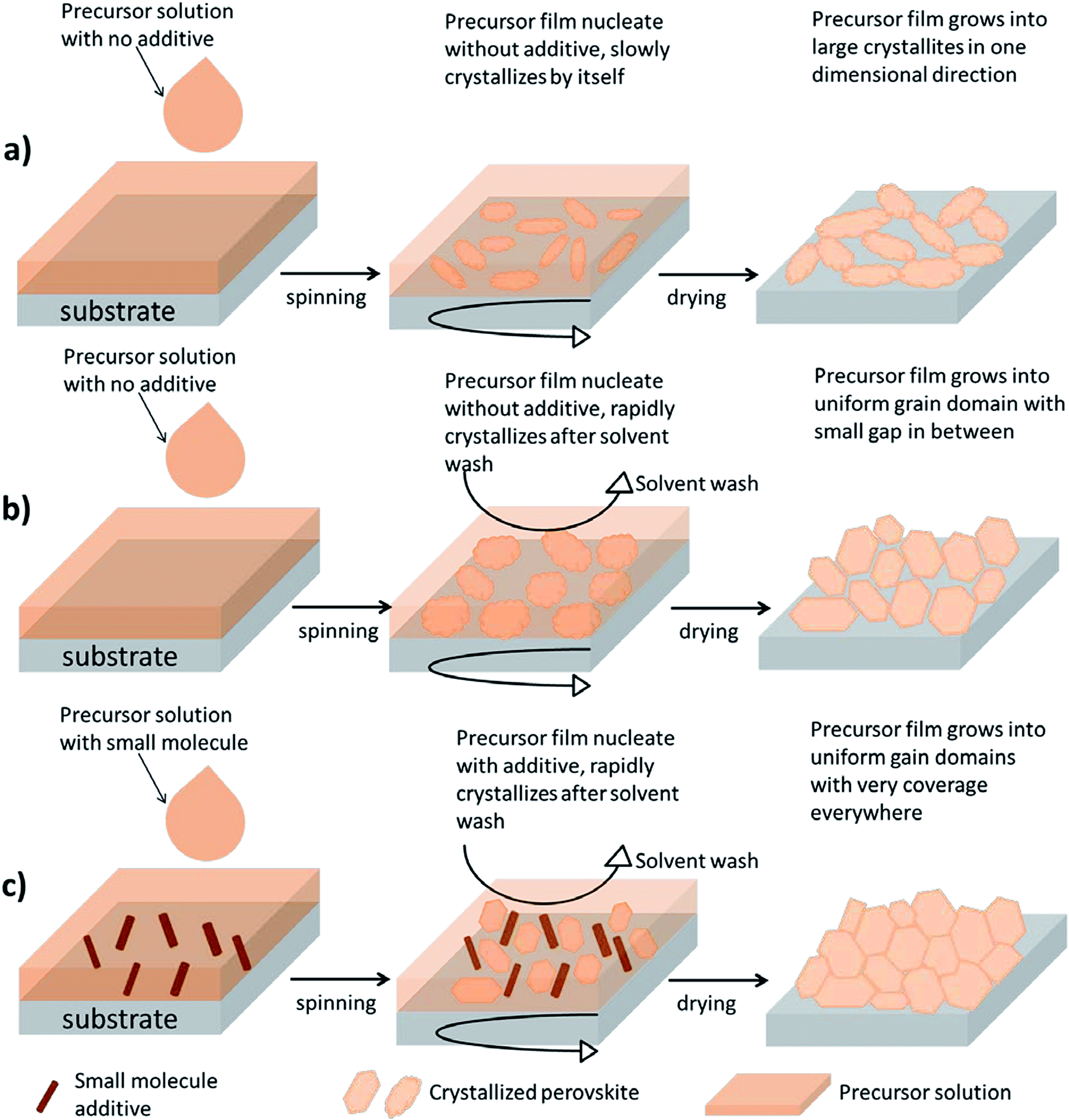 | ||
| Fig. 1 (a) Non-modified procedure for preparing the perovskite film without solvent wash and additive; (b) solvent wash procedure for preparing the perovskite film; and (c) additive-assisted solvent wash procedure for preparing the perovskite film. | ||
One simple way to solve this problem is through the manipulation of the rate of crystallite growth during spin-coating. Fig. 1b and c demonstrate two methods of incorporating an extra step of solvent washing during the spin-coating to induce instant crystallization of an intermediate phase (CH3NH3I–PbI2) and thus the surface coverage of the precursor film can be maximized. Here, the role of the nonpolar solvent can be described as a morphological catalyst. Seok et al., have found that during the spin-coating process the dropping of a non-polar solvent, such as toluene, can immediately reduce the original solvent content in the precursor film and thus force crystallites to precipitate instantly.28 The resulting film morphology typically has a more uniform grain domain and improved surface coverage (Fig. 1b). This second method is hereafter known as the “solvent wash method”.
Here, we introduce a third method by modifying the second method in order to improve its reproducibility and, at the same time, further eliminate the formation of small voids. In the original solvent wash method, it was found that toluene had to be dropped after a certain duration of time during spin coating (e.g. 6 seconds). Within these 6 seconds, the nucleation of a precursor-intermediate phase is initiated and small crystallites begin to precipitate out. We proposed that the addition of small molecules, such as 1,3-bis[3,5-di(pyridin-3-yl)phenyl]benzene (BmPyPhB), can enhance the initial nucleation process by providing heterogeneous nucleation sites for the precursor species throughout the space. Thus, with numerous nucleates uniformly distributed in the film, the resulting precursor crystallites grown using this setup are expected to be even more compact and void-free (Fig. 1c), compared to those obtained from the original solvent wash method (Fig. 1b). We hereafter describe this third method as the “additive-assisted solvent wash method”.
Fig. 2 shows AFM and SEM images corresponding to the non-modified, solvent wash, and additive-assisted solvent wash perovskite thin films on PEDOT:PSS prior to the annealing treatment. Fig. 2a–c show AFM height images, and Fig. 2d–f show the corresponding SEM images. Starting with Fig. 2a and d, the non-modified CH3NH3PbI3 film obtained via the one-step deposition process is characterized. The morphology of this perovskite film has a large roughness and low surface coverage. Moreover, there is a clear indication of needle-like crystallites, meaning that the crystal growth mainly occurred in a one-dimensional (1D) direction.29 We suspect that such an unfavorable morphology is mainly due to the lack of nucleation sites, which promotes the formation of large crystallites, and slow crystal growth that allows nanocrystals to grow into nanoneedles.
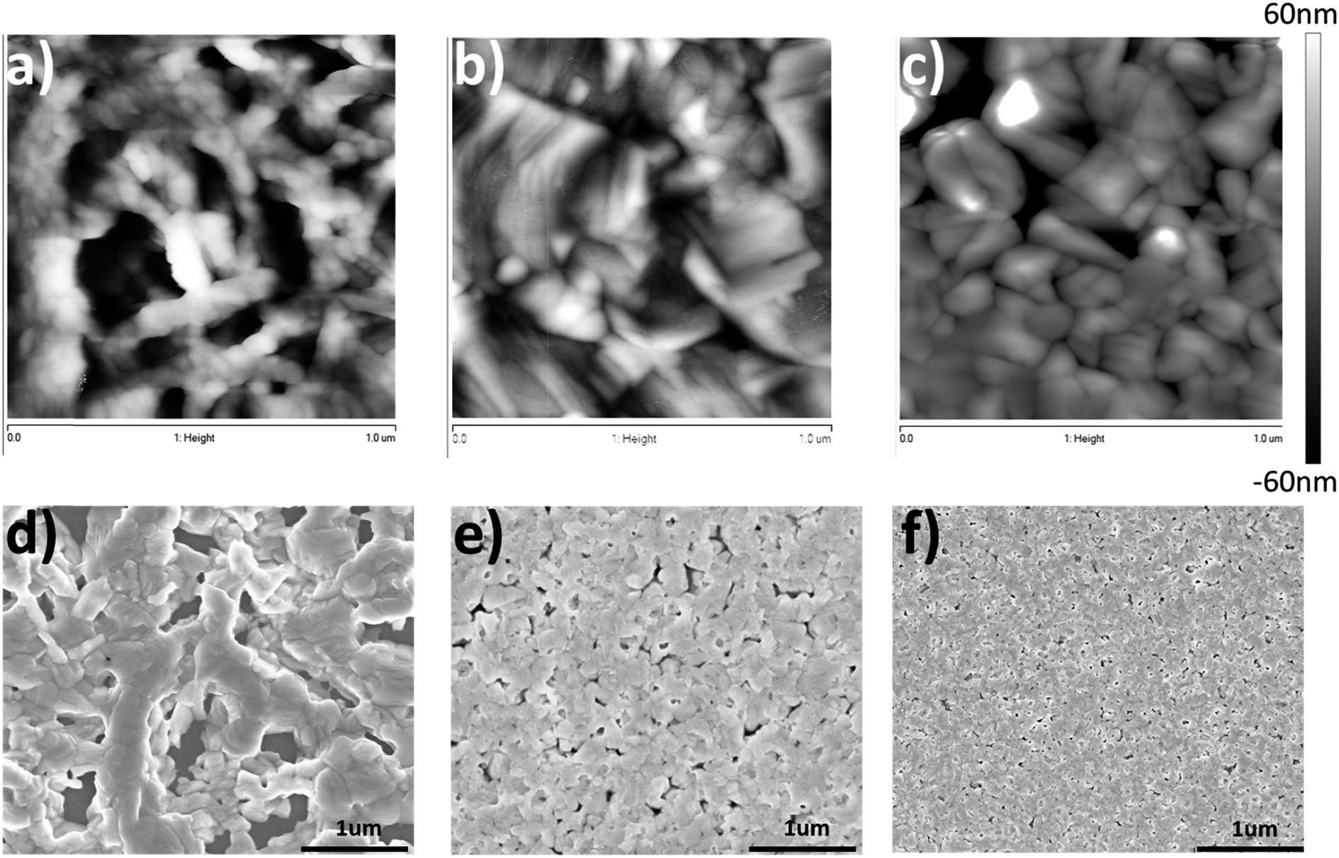 | ||
| Fig. 2 AFM topography of the perovskite film prior to thermal annealing processed from (a) non-modified, (b) solvent wash, and (c) additive-assisted solvent wash methods; similarly, SEM topography of the perovskite films post thermal annealing from (d) non-modified, (e) solvent wash, and (f) additive-assisted solvent wash methods. The size of the AFM images is 1 × 1 μm2. The scale bar for the SEM images is 1 μm. | ||
In Fig. 2b and e, solvent washed CH3NH3PbI3 films via the one-step deposition method are characterized. From the AFM height images, the surface roughness of the perovskite is greatly reduced making it free from large voids that were previously found in the non-modified samples. When the nonpolar solvent (e.g. toluene) is applied onto the precursor film during spin-coating, the precursor species that are not soluble in toluene are forced to crystallize and immediately precipitate. Therefore, crystal growth is accelerated and finished right after the solvent wash. Consequently, no prolonged heating is required since perovskite crystallites are already mostly formed. Furthermore, the absence of a needle-like morphology also indicates that crystal growth is not confined in 1D anymore. From the SEM image, the surface coverage is greatly improved; however, there are still small voids throughout the film. In Fig. 2c and f, the additive-assisted solvent washed CH3NH3PbI3via the one-step deposition method is characterized. The AFM image indicates that the perovskite film is further planarized with adding BmPyPhB into the precursor formulation. The grain size is smaller and more compact compared to that observed using the original solvent wash method, which can be ascribed to the increase of heterogeneous nucleation sites provided by BmPyPhB during crystal growth. Most importantly, from the SEM image the number and size of the voids are further reduced, making this method even more suitable for solution based device fabrication at low temperature.
Fig. 3a and b show the device structure and energy level diagram for a planar-structured single junction perovskite solar cell. The photocurrent density and voltage curves (J–V) for a perovskite solar cell in a planar single junction are given in Fig. 3c and d. In Fig. 3c, the perovskite planar junction is prepared using the 3 different film growth methods introduced in Fig. 1, e.g. the non-modified, solvent wash, and additive-assisted solvent wash methods. A summary of the performance parameters and thickness variations is listed in Table 1. In Fig. 2c, the open-circuit voltage (VOC) of the non-modified samples shows a major reduction compared to that obtained for samples made using the other two processing conditions, which can be ascribed to the possible non-continuous film morphology along with increased charge recombination. The poor fill factor (FF) also indicates that the charge transport is obstructed by compromised interfacial contacts with electrodes due to limited surface coverage. As a result, an unfavorable morphology obtained from the non-modified precursor solution makes the PCE of devices only as efficient as 4.7%.
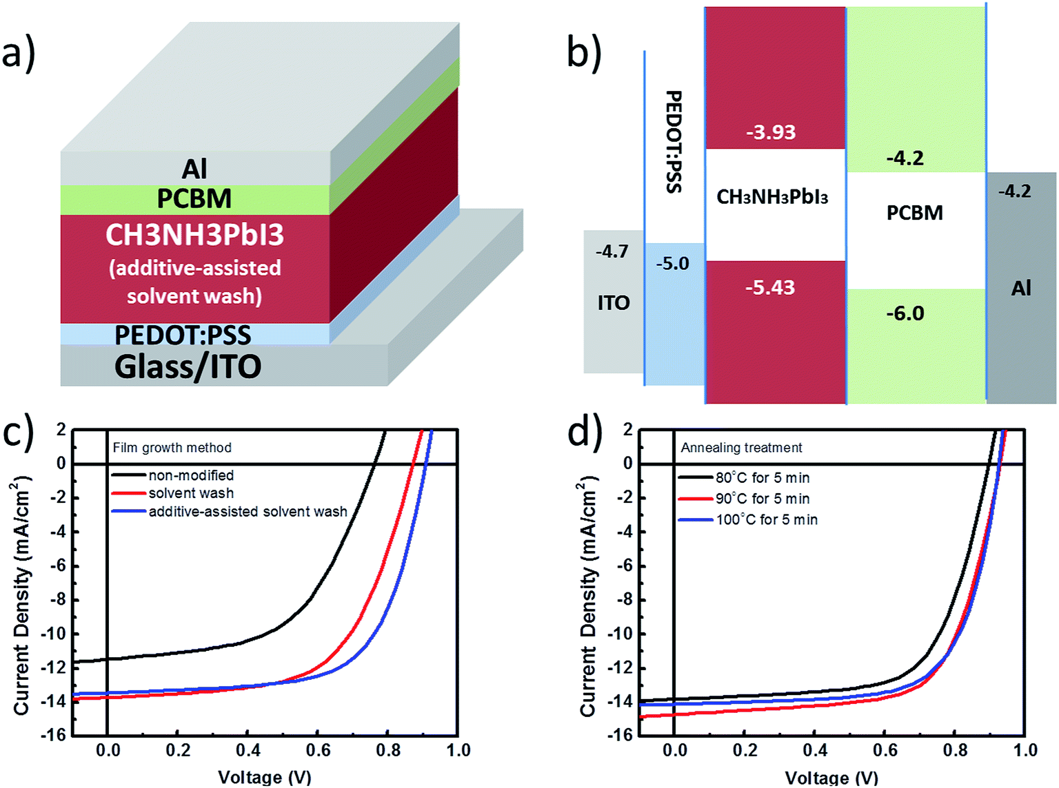 | ||
| Fig. 3 (a) Device architecture of the planar structure perovskite solar cell (glass/ITO/PEDOT:PSS/perovskite layer/PCBM/Al); (b) proposed energy level landscape for the perovskite solar cell; (c) J–V curves for a single junction cell processed via different methods; (d) J–V curves for a single junction cell processed via different annealing temperatures. | ||
| CH3NH3PbI3 single junction | ||||
|---|---|---|---|---|
| Film growth method | V OC (V) | J SC (mA cm−2) | FF | PCE (%) |
| Non-modified | 0.76 | 11.5 | 0.54 | 4.72 |
| Solvent wash | 0.88 | 13.8 | 0.60 | 7.28 |
| Additive-assisted solvent wash | 0.90 | 13.4 | 0.66 | 7.95 |
| CH3NH3PbI3 single junction | ||||
|---|---|---|---|---|
| Annealing treatment | V OC (V) | J SC (mA cm−2) | FF | PCE (%) |
| 80 °C for 5 min | 0.90 | 13.7 | 0.65 | 8.01 |
| 90 °C for 5 min | 0.92 | 14.6 | 0.67 | 8.99 |
| 100 °C for 5 min | 0.92 | 14.1 | 0.70 | 9.08 |
| PBSeDTEG8 single junction | ||||
|---|---|---|---|---|
| Annealing treatment | V OC (V) | J SC (mA cm−2) | FF | PCE (%) |
| Non-annealed | 0.67 | 15.2 | 0.69 | 7.03 |
| 100 °C for 5 min | 0.66 | 14.7 | 0.68 | 6.62 |
| Hybrid tandem junction | ||||
|---|---|---|---|---|
| Cathode choice | V OC (V) | J SC (mA cm−2) | FF | PCE (%) |
| Al only | 1.51 | 9.91 | 0.61 | 9.13 |
| PFN/Al | 1.52 | 10.05 | 0.67 | 10.23 |
On the other hand, the solvent washed samples show a great improvement in both the short-circuit current density (JSC) and FF values, resulting in 7.2% PCE. Since both the JSC and FF values are directly related to the charge collection capability, it is reasonable to believe that the morphology of the perovskite film after solvent washing becomes more favorable for device fabrication. Finally, when compared with the solvent washed samples, a further 10% improvement in the PCE is observed for the additive-assisted solvent washed samples at 7.9%, which we mainly ascribed to the effect of adding small molecules thus changing the nucleation process and resulting final morphology. In conclusion from this, the effectiveness of using the solvent wash method as a morphology modifier for perovskites has been validated through photovoltaic performance as shown above. The incorporation of BmPyPhB as an additive in the solution processing in order to further enhance the performance also supports our claim that a small molecule additive in the precursor solution can be an another effective way to control morphology.
In Fig. 3d, a series of three different annealing temperatures are used for a short duration of time (e.g. 5 minutes) to convert the precursor film from the intermediate phase to the perovskite phase based on the additive-assisted solvent wash method. By increasing the temperature from 80 °C to 100 °C, the resulting device performance can be further improved from 7.9% to 9.1% PCE. Although the most efficient devices are still those baked at 100 °C, the samples processed at 80 °C can maintain up to 86% of the best efficiency achieved by those processed at 100 °C. Thus, this observation specifies a weak dependence of device performance on the annealing temperature which can be mainly attributed to a well crystallized perovskite phase induced by both solvent wash and small molecule additive methods prior to the annealing treatment. Therefore, no prolonged and high temperature annealing treatment is required for achieving an optimized morphology for the perovskite thin film.
3. Perovskite/polymer hybrid tandem solar cell
Fig. 4a demonstrates a device design for realizing a highly efficient hybrid tandem solar cell composed of perovskite and polymer absorbers. Due to the high absorption coefficient (1 × 105 cm−1) of perovskite CH3NH3PbI3 compared to that of a polymer (6 × 104 cm−1),30 we placed IR-polymers and fullerene derivatives as the bottom subcell absorbers in tandem devices to catch the incident light first, while the perovskite CH3NH3PbI3 as a top subcell absorber can harness the remaining photons. Such an arrangement of absorbers in tandem intends to balance the photocurrent generation from the subcells and have a matched current density for maximizing the overall device performance. In Fig. 4b, the photon absorption profiles for each subcell in tandem are provided with their calculated short-circuit current (JSC). The optimal thickness adjustments for each subcell are found to be around 90–105 nm for the polymer in the bottom subcell and 180–190 nm for the perovskite in the top subcell.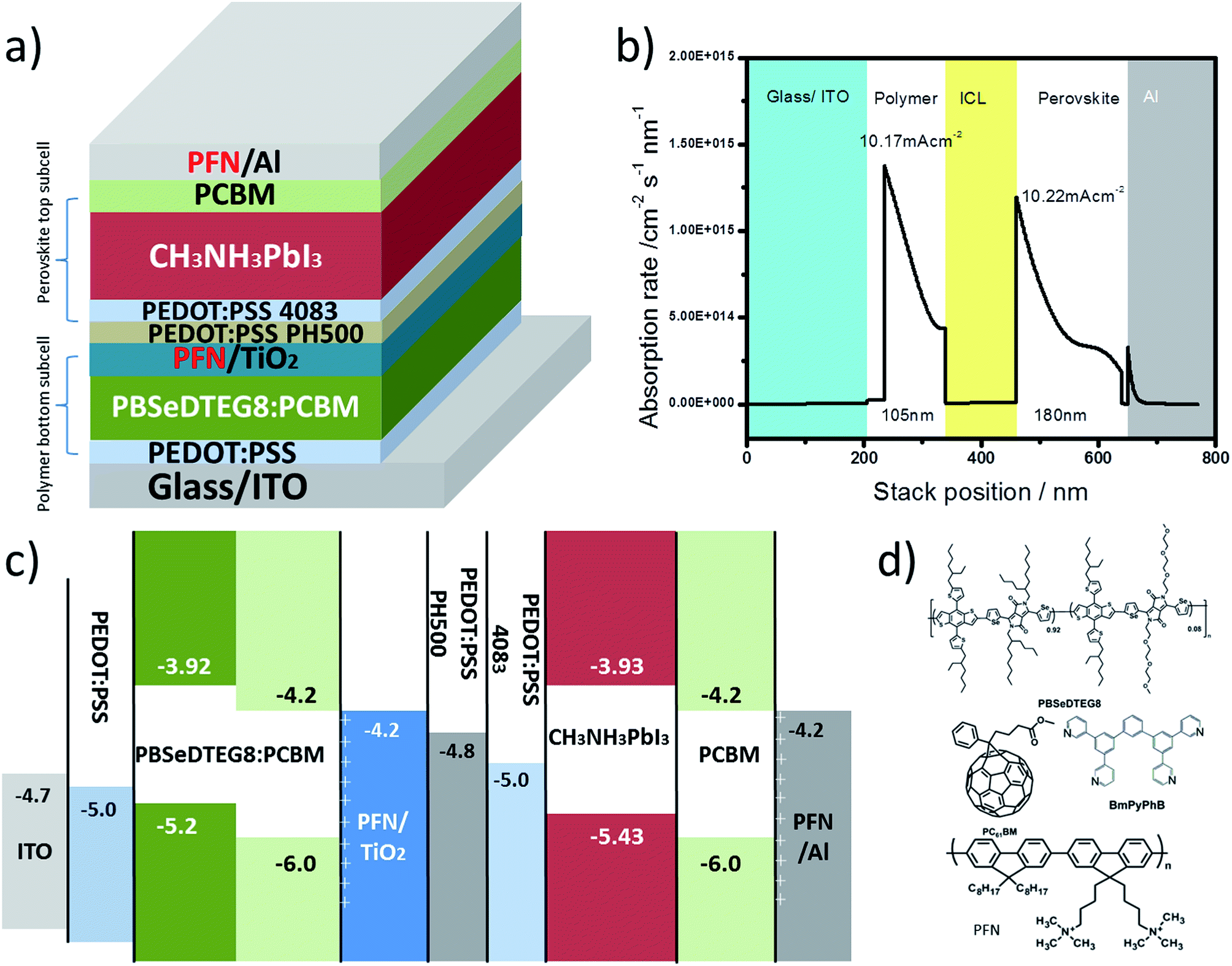 | ||
| Fig. 4 (a) Device architecture of the hybrid tandem solar cell composed of perovskite and polymer absorbers; (b) photon absorption rate profile for each subcell inside hybrid tandem solar cell; (c) proposed energy level landscape for the hybrid tandem solar cell; (d) chemical structures of PBSeDTEG8, PCBM, BmPyPhB, and PFN. | ||
Fig. 4c shows the band diagram of the complete hybrid tandem solar cell. In between the two subcells, the recombination layers are presented to function as electrical connections and to facilitate efficient charge recombination. Here, we presented a design of recombination layers based on a metal oxide, PEDOT:PSS, and a conjugated polyelectrolyte made of poly[(9,9-bis(3′-(N,N-dimethylamino)propyl)-2,7-fluorene)-alt-2,7-(9,9-dioctylfluorene)] (PFN) all processed using solution methods. Particularly for the perovskite subcell, double electron and hole interlayers are introduced. PCBM with a LUMO of 4.2 eV and PFN with a surface dipole are used as electron transporting and hole blocking layers, respectively, to efficiently draw electrons out from the perovskite absorbers and to minimize interfacial recombination.31 Similarly, double hole transporting layers can also be realized here using PEDOT:PSS PH500 and AI 4083 as hole transporting and electron blocking layers, respectively.10 AI 4083 with a deeper work function (5.0 eV) and higher resistivity (100 Ω □−1) can block electrons more efficiently than PH500.
Besides the arrangement of absorbers and the design of the recombination layers, the processing compatibility between the perovskite and the polymer presents another great challenge in demonstrating a successful hybrid tandem solar cell. Particularly for polymer absorbers used in the bottom subcell, thermal stability is required in order to survive the thermal treatment (100 °C for 5 min) during the process of forming the CH3NH3PbI3 perovskite phase. Here, we presented an alternative to the popular narrow-bandgap polymer, PBDTT-SeDPP,32 in the form of a block copolymer, namely PBSeDTEG8. The chemical structures of the PBSeDTEG8 absorbers used in the bottom subcells are shown in Fig. 4d. Here, we found that the PBSeDTEG8:PCBM photoactive layer can be processed without an additive (such as DIO, CN) and still reach its optimal performance. This can be ascribed to its triethylene glycol side chain which can reinforce the stacking order of the polymer chain thus maintaining a stable photovoltaic performance at an elevated temperature.33 From Table 1, a PBSeDTEG8:PCBM single junction solar cell in a pristine state, without annealing, can achieve 7.0% PCE. When annealed at 100 °C for 5 min, there is a slight drop in performance but it is still kept at 6.6% PCE.
Next, we examine the photovoltaic performance of the hybrid tandem solar cell composed of perovskite and polymer absorbers. Here, two different top electrodes are compared to identify the improvement resulting from the use of PFN as an electrode interlayer. In Fig. 5a, the J–V curve results show that with a reflective Al (Al-based) electrode and a thick layer of perovskite (180 nm) as a back subcell, the hybrid tandem solar cell can attain its highest PCE = 9.13% at VOC = 1.51 V, JSC = 9.91 mA cm−2 and FF = 0.61. The VOC of the hybrid tandem solar cell is close to the sum of the VOC of the perovskite (0.92 V) and the polymer (0.66 V) subcells owing to the efficient recombination at interconnecting layers and negligible voltage loss for aligning the Fermi level between the subcells. Furthermore, a modification of the top electrode with PFN (PFN-based) is also demonstrated. In this setup, a thin layer of PFN is inserted between PCBM and the Al electrode to improve the electron injection to the electrode. The resulting performance shows VOC = 1.52 V, JSC = 10.05 mA cm−2, FF = 0.67, and a PCE = 10.23%. The photocurrent density of the PFN-based top electrode hybrid tandem solar cell is higher than that of the Al-based top electrode hybrid tandem solar cell owing to the presence of PFN as a dipole layer that can efficiently lower the injection barrier for electrons and block holes at the same time, thus interfacial recombination is reduced. With the results obtained, we have successfully demonstrated a monolithic hybrid tandem solar cell composed of perovskite and polymer absorbers fabricated using a full solution process.
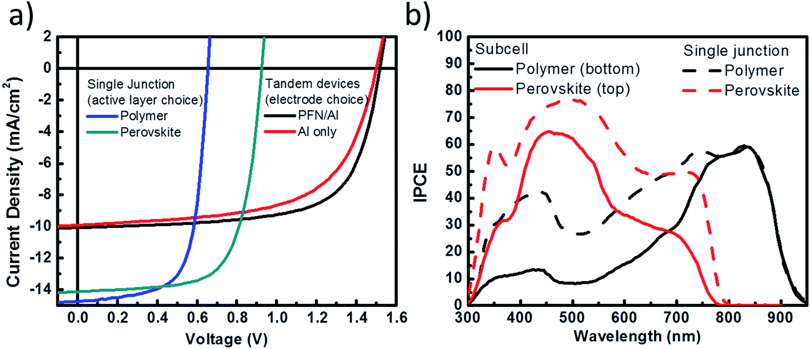 | ||
| Fig. 5 (a) J–V curves for the hybrid tandem device made using different cathodes and for different perovskite and polymer absorbers in a single junction setup; (b) the external quantum efficiency of the perovskite and polymer subcells measured in the hybrid tandem device (solid lines) and of single junction reference devices made using the same thickness of perovskite and polymer layers (dashed lines). | ||
Furthermore, we took the EQE measurement for the PFN-based optimized tandem solar cells. The EQE measurement for each subcell is provided in Fig. 5b. To obtain accurate EQE results, one subcell is selectively turned on by monochromatic light bias while another subcell is measured.34 The integrated current density from EQE is 9.9 mA cm−2 for the bottom polymer subcell and 9.85 mA cm−2 for the top subcell, which are in a good agreement with both J–V characteristics and optical simulations. The reference EQE results for single junction perovskite and polymer solar cells are provided in the same figure. Moreover, the J–V characteristics of single junction cells measured under the influence of optical interference, similar to that experienced by the subcells in the hybrid tandem structure, are also provided in the ESI.† The JSC values are in good agreement with calculated JSC values from the EQE measurement. These results suggest that our design of recombination layers has provided an optimized connection between the two subcells with the least optical or electrical losses.
4. Conclusion
In conclusion, we have demonstrated efficient hybrid tandem solar cells by integrating perovskite and polymer:fullerene as subcell absorbers. For the cell integrating a perovskite as an absorber, CH3NH3PbI3 with a photosensitivity up to 800 nm is utilized. To further improve the morphology of the perovskite and to reduce the requirement of thermal treatment, the solvent wash method is applied to control the crystal growth process along with the small molecule additive BmPyPhB, as a source of heterogeneous nucleation sites to provide a continuous and dense morphology without large voids. With a fine morphology, the CH3NH3PbI3 single junction cell can attain a 9.1% PCE using a very mild thermal treatment of 100 °C for 5 minutes. In terms of recombination layers, double hole and double electron transporting layers are applied. More importantly, all of these interlayers are solution processable and thus maintain the orthogonal processing advantages for hybrid tandem solar cells.Finally, we introduced a new IR-polymer, PBSeDTEG8 with excellent thermal tolerance as the bottom subcell in our tandem devices. The hybrid tandem cell of this design can achieve an optimal efficiency of 9.13% which is greater than both of the perovskite and polymer single junction cells used in our study. To further improve the contact with the Al electrode, PFN as interfacial dipole layer is applied prior to the top electrode deposition. Device performance shows a promising improvement with a higher FF value and a greater efficiency of 10.23%. In summary, the developments presented here have provided guidelines for designing effective tandem devices from solution-processed organic polymer materials and inorganic hybrid perovskite materials. Our work suggests that there is a promising future for solution-based hybrid tandem solar cells using a perovskite as a building block. We expect that the PCE of this perovskite/polymer hybrid tandem system could reach 15% or above when new a IR polymer with 10–12% PCE in the single junction is realized and incorporated.
5. Experimental section
Single junction solar cell
The device architecture of the single junction cell is shown in Fig. 2a. The devices were fabricated on ITO-coated glass substrates, with a sheet resistance of 15 Ω □−1. The pre-cleaned ITO substrates were treated with UV-ozone and then spin-coated with the PEDOT:PSS AI 4083 solution by baking at 140 °C for 10 min in ambient air. The samples were then transferred to a nitrogen-filled glove box for perovskite and polymer deposition. For the polymer, an active layer of ∼100 nm thickness was deposited by spin-coating PBSeDTEG8:PC61BM from a 1![[thin space (1/6-em)]](https://www.rsc.org/images/entities/char_2009.gif) :2 wt. ratio DCB solution. The Ca/Al (20 nm/100 nm) electrode was thermally evaporated through a shadow mask. For the perovskite, an active layer of various thicknesses was deposited by spin-coating CH3NH3I:PbI2 from a 1:1 molar ratio DMF solution (42 wt%) at 4000 rpm for 60 s. For the small molecule additive-containing solution, there was 3% of BmPyPhB with respect to CH3NH3I:PbI2. During the rotation, after 6 s, one drop of 20 μL of toluene solvent was dropped on the sample and there was an immediate change from transparent to a brownish color.28 The samples were annealed at 100 °C for 5 min.29 The PCBM solution (2 wt% in chlorobenzene) was spin-coated to form a 50 nm layer.35 Finally, 100 nm of Al was thermally evaporated through a shadow mask. The device area, as defined by the overlap between the ITO and Al electrodes, was 0.100 cm2. The non-overlapping area was scratched out using a razor blade to avoid the overestimation of JSC.
:2 wt. ratio DCB solution. The Ca/Al (20 nm/100 nm) electrode was thermally evaporated through a shadow mask. For the perovskite, an active layer of various thicknesses was deposited by spin-coating CH3NH3I:PbI2 from a 1:1 molar ratio DMF solution (42 wt%) at 4000 rpm for 60 s. For the small molecule additive-containing solution, there was 3% of BmPyPhB with respect to CH3NH3I:PbI2. During the rotation, after 6 s, one drop of 20 μL of toluene solvent was dropped on the sample and there was an immediate change from transparent to a brownish color.28 The samples were annealed at 100 °C for 5 min.29 The PCBM solution (2 wt% in chlorobenzene) was spin-coated to form a 50 nm layer.35 Finally, 100 nm of Al was thermally evaporated through a shadow mask. The device area, as defined by the overlap between the ITO and Al electrodes, was 0.100 cm2. The non-overlapping area was scratched out using a razor blade to avoid the overestimation of JSC.
Hybrid tandem solar cell
The device architecture of the hybrid tandem cell is shown in Fig. 4a. The tandem devices were fabricated on ITO-coated glass substrates, with a sheet resistance of 15 Ω □−1. First, the procedure follows the fabrication of the single junction solar cell for the polymer, without depositing the electrode. Then, inside the glovebox the interconnecting layers (ICLs) used as recombination layers in tandem are formed. Firstly, a 5 nm thickness surface dipole layer was spin-coated from 0.02 wt% PFN solution in methanol.10 Next, ICL of 30 nm thickness was deposited by spin-coating a TiO2 nanoparticle precursor solution from 0.2 wt% ethanol solution.17 The samples were annealed at 100 °C for 2 min. The PEDOT:PSS PH500 was spin-coated to form a 60 nm layer, and annealed at 100 °C for 1 min. Similarly, the PEDOT:PSS AI 4083 was spin-coated to form a 30 nm layer, and annealed at 100 °C for 1 min. The second active layer was spin-coated at 4000 r.p.m. for 60 s from CH3NH3I:PbI2 (1:1 molar ratio) with 3% BmPyPhB in DMF solution (29 wt%). The samples were solvent washed with toluene during the spin-coating and annealed at 100 °C for 5 min. Lastly, 5 nm of PFN was deposited using the same methanol solution. Finally, to complete the solar cell device, 100 nm of aluminum as the anode was thermally evaporated through a shadow mask. The device area, as defined by the overlap between the ITO and Al electrodes, was 0.100 cm2. The non-overlapping area was scratched out using a razor blade to avoid the overestimation of JSC.
Solar cell device measurement
The device layout is provided in the supporting information to show how the actual tandem devices were measured. The current density–voltage (J–V) characteristic curve of the solar cells were measured with a 0.1 cm2 shadow mask using a Keithley 2400 SourceMeter under a simulated AM1.5G solar illumination from a Newport solar simulator setup. A KG-5 filter silicon photodiode was used to calibrate the light intensity to 1 sun (100 mW cm−2). To avoid overestimating the photocurrent, each device was isolated completely by scratching the surrounding films around the device.9 External quantum efficiencies (EQEs) were measured using an Enlitech QE-R spectral response measurement system. An SRC-2020 solar reference cell was used to calibrate the EQE measurement spectrum. AFM and SEM measurements were performed in the Nano & Pico Characterization Lab at California Nano Systems Institute and at Nanolab, respectively. The PL photons were counted using a Picoharp 300 after pre-amplification using a PAM102.Acknowledgements
This work was financially supported by the Air Force Office of Scientific Research (AFOSR, Grant no. FA9550-09-1-0610), National Science Foundation (NSF ECCS-1202231), and UCLA internal funds. We would like to thank Mr Wei-Hsuan Chang for synthesizing the low band gap polymer and Dr Huanping Zhou for synthesizing MAI. We would also like to thank Dr Zirou Hong, Dr Gang Li, and Dr Qi Chen for proofreading the manuscript. Finally, the authors also thank the Nano & Pico Characterization Lab at CNSI for the AFM measurements and Enlitech Co., Ltd., for providing the EQE measurement equipment. C.C.C. would like to give thanks for an NSF-funded IGERT: Clean Energy for Green Industry Fellowship (Grant DGE-0903720).References
- A. Kojima, K. Teshima, Y. Shirai and T. Miyasaka, J. Am. Chem. Soc., 2009, 131, 6050–6051 CrossRef CAS PubMed.
- M. M. Lee, J. Teuscher, T. Miyasaka, T. N. Murakami and H. J. Snaith, Science, 2012, 338, 643–647 CrossRef CAS PubMed.
- J. Burschka, N. Pellet, S.-J. Moon, R. Humphry-Baker, P. Gao, M. K. Nazeeruddin and M. Grätzel, Nature, 2013, 499, 316–319 CrossRef CAS PubMed.
- J. H. Heo, S. H. Im, J. H. Noh, T. N. Mandal, C.-S. Lim, J. A. Chang, Y. H. Lee, H.-j. Kim, A. Sarkar and M. K. Nazeeruddin, Nat. Photonics, 2013, 7, 486–491 CrossRef CAS.
- M. Liu, M. B. Johnston and H. J. Snaith, Nature, 2013, 501, 395–398 CrossRef CAS PubMed.
- H. Zhou, Q. Chen, G. Li, S. Luo, T.-b. Song, H.-S. Duan, Z. Hong, J. You, Y. Liu and Y. Yang, Science, 2014, 345, 542–546 CrossRef CAS PubMed.
- M. A. Green, A. Ho-Baillie and H. J. Snaith, Nat. Photonics, 2014, 8, 506–514 CrossRef CAS.
- J. H. Noh, S. H. Im, J. H. Heo, T. N. Mandal and S. I. Seok, Nano Lett., 2013, 13, 1764–1769 CAS.
- C. C. Chen, W. H. Chang, K. Yoshimura, K. Ohya, J. You, J. Gao, Z. Hong and Y. Yang, Adv. Mater., 2014, 26, 5670–5677 CrossRef CAS PubMed.
- C.-C. Chen, L. Dou, J. Gao, W.-H. Chang, G. Li and Y. Yang, Energy Environ. Sci., 2013, 6, 2714–2720 CAS.
- N. K. Noel, S. D. Stranks, A. Abate, C. Wehrenfennig, S. Guarnera, A. Haghighirad, A. Sadhanala, G. E. Eperon, S. K. Pathak, M. B. Johnston, A. Petrozza, L. M. Herz and H. J. Snaith, Energy Environ. Sci., 2014, 7, 3061–3068 CAS.
- F. Hao, C. C. Stoumpos, D. H. Cao, R. P. Chang and M. G. Kanatzidis, Nat. Photonics, 2014, 8, 489–494 CrossRef CAS.
- M. H. Kumar, S. Dharani, W. L. Leong, P. P. Boix, R. R. Prabhakar, T. Baikie, C. Shi, H. Ding, R. Ramesh, M. Asta, M. Grätzel, S. G. Mhaisalkar and N. Mathews, Adv. Mater., 2014, 26, 7122–7127 CrossRef CAS PubMed.
- F. Zuo, S. T. Williams, P. W. Liang, C. C. Chueh, C. Y. Liao and A. K. Y. Jen, Adv. Mater., 2014, 26, 6454–6460 CrossRef CAS PubMed.
- F. Hao, C. C. Stoumpos, R. P. Chang and M. G. Kanatzidis, J. Am. Chem. Soc., 2014, 136, 8094–8099 CrossRef CAS PubMed.
- S. Chen, J. R. Manders, S.-W. Tsang and F. So, J. Mater. Chem., 2012, 22, 24202–24212 RSC.
- C. C. Chen, L. Dou, R. Zhu, C. H. Chung, T. B. Song, Y. B. Zheng, S. Hawks, G. Li, P. S. Weiss and Y. Yang, ACS Nano, 2012, 6, 7185–7190 CrossRef CAS PubMed.
- L. Dou, C.-C. Chen, K. Yoshimura, K. Ohya, W.-H. Chang, J. Gao, Y. Liu, E. Richard and Y. Yang, Macromolecules, 2013, 46, 4734–4734 CrossRef CAS.
- O. Malinkiewicz, A. Yella, Y. H. Lee, G. M. Espallargas, M. Grätzel, M. K. Nazeeruddin and H. J. Bolink, Nat. Photonics, 2014, 8, 128–132 CrossRef CAS.
- P. Docampo, J. M. Ball, M. Darwich, G. E. Eperon and H. J. Snaith, Nat. Commun., 2013, 4, 2761 Search PubMed.
- E. Edri, S. Kirmayer, A. Henning, S. Mukhopadhyay, K. Gartsman, Y. Rosenwaks, G. Hodes and D. Cahen, Nano Lett., 2014, 14, 1000–1004 CrossRef CAS PubMed.
- Q. Wang, Y. Shao, Q. Dong, Z. Xiao, Y. Yuan and J. Huang, Energy Environ. Sci., 2014, 7, 2359–2365 CAS.
- Z. Xiao, C. Bi, Y. Shao, Q. Dong, Q. Wang, Y. Yuan, C. Wang, Y. Gao and J. Huang, Energy Environ. Sci., 2014, 7, 2619–2623 CAS.
- J. You, Z. Hong, Y. Yang, Q. Chen, M. Cai, T.-B. Song, C.-C. Chen, S. Lu, Y. Liu, H. Zhou and Y. Yang, ACS Nano, 2014, 8, 1674–1680 CrossRef CAS PubMed.
- A. Dualeh, N. Tétreault, T. Moehl, P. Gao, M. K. Nazeeruddin and M. Grätzel, Adv. Funct. Mater., 2014, 24, 3250–3258 CrossRef CAS.
- Y. Zhao and K. Zhu, J. Phys. Chem. C, 2014, 118, 9412–9418 CAS.
- G. Griffini, J. D. Douglas, C. Piliego, T. W. Holcombe, S. Turri, J. M. Fréchet and J. L. Mynar, Adv. Mater., 2011, 23, 1660–1664 CrossRef CAS PubMed.
- N. J. Jeon, J. H. Noh, Y. C. Kim, W. S. Yang, S. Ryu and S. I. Seok, Nat. Mater., 2014, 13, 897–903 CrossRef CAS PubMed.
- M. Xiao, F. Huang, W. Huang, Y. Dkhissi, Y. Zhu, J. Etheridge, A. Gray-Weale, U. Bach, Y. B. Cheng and L. Spiccia, Angew. Chem., 2014, 126, 10056–10061 CrossRef.
- J. Yan and B. R. Saunders, RSC Adv., 2014, 4, 43286–43314 RSC.
- H. Zhang, H. Azimi, Y. Hou, T. Ameri, T. Przybilla, E. Spiecker, M. Kraft, U. Scherf and C. J. Brabec, Chem. Mater., 2014, 26, 5190–5193 CrossRef CAS.
- L. Dou, W. H. Chang, J. Gao, C. C. Chen, J. You and Y. Yang, Adv. Mater., 2013, 25, 825–831 CrossRef CAS PubMed.
- W. H. Chang, J. Gao, L. Dou, C. C. Chen, Y. Liu and Y. Yang, Adv. Energy Mater., 2014, 26, 3142–3147 CrossRef PubMed.
- L. Dou, J. You, J. Yang, C.-C. Chen, Y. He, S. Murase, T. Moriarty, K. Emery, G. Li and Y. Yang, Nat. Photonics, 2012, 6, 180–185 CrossRef CAS.
- C. Zuo and L. Ding, Nanoscale, 2014, 6, 9935–9938 RSC.
Footnote |
| † Electronic supplementary information (ESI) available. See DOI: 10.1039/c4mh00237g |
| This journal is © The Royal Society of Chemistry 2015 |