
Visually tolerable tiling (VTT) for making a large-area flexible patterned surface†
Moon Kyu
Kwak‡
a,
Jong G.
Ok‡
 bc,
Sung Ho
Lee
a and
L. Jay
Guo
*c
bc,
Sung Ho
Lee
a and
L. Jay
Guo
*c
aSchool of Mechanical Engineering, Kyungpook National University, Daegu 702-701, Korea
bDepartment of Mechanical and Automotive Engineering, Seoul National University of Science and Technology, 232 Gongneung-ro, Nowon-gu, Seoul 139-743, Korea
cDepartment of Mechanical Engineering, Department of Electrical Engineering and Computer Science, University of Michigan, Ann Arbor, Michigan 48109, USA. E-mail: guo@umich.edu; Fax: +1-734-763-9324; Tel: +1-734-764-3345
First published on 30th September 2014
Abstract
The fabrication of a large area mold is one of the most difficult challenges in the roll to roll nanoimprint field and eliminating the visible seams on a large area mold is even more difficult. We present a visually tolerable tiling (VTT) method to make large area micro/nano-patterns without visible seams and their applications. In this study, with small area micro/nano-pattern molds, the VTT method could produce a scaled up mold with the same features as the original mold without any visible seam lines. Also, a fabricated large size mold was used in the roll to roll imprinting process as a flexible mold. By using the VTT method, large size metal wire grid polarizers and micro-prism sheets were fabricated and their potential was confirmed as feasible applications.
Conceptual insightsThe most serious limitation of the nanoimprint method (especially for large area roll to roll nanoimprint) is the size of the nanoimprint mold. This is because the master mold is typically fabricated by conventional lithography techniques, e.g. e-beam lithography. With the replication technique introduced in this work, the imprint method can be free from the master size issue for many optical structure fabrications. In this work, a visually tolerable tiling (VTT) method is developed and a quasi-seamless large area micro/nano-patterned surface is fabricated. The fabricated flexible large area mold was used in a roll to roll imprint process and large area metal wire grid polarizers and micro-prism sheets were fabricated as feasible applications. Also, surface energy analysis was done to explain how the VTT method can be realized. The development of the VTT method could enable the imprint process for mass production in practical applications. |
Increasing demands of large-area micro- and nano-scale structures in many applications have spurred the development of new techniques targeting scalability.1–5 Roll-to-Roll (R2R) nanoimprinting (NIL) is a primary example of such developments, which promises high-speed micro/nano-patterning over large areas in a continuous fashion. Due to the challenge of making large-area NIL molds, large area R2R NIL stamps have mostly been limited to the use and stitching of multiple smaller stamps.1 However in some applications, the stitching seams can cause problems, such as stress concentrations in mechanical components, trapping of liquid in fluidic products, and poor contact spots in continuous patterning production.
Especially in the field of display devices, visible seams between the zones often seriously impair the visual performance of the structure and should be avoided. As a specific example, a polarizer is an essential component in liquid crystal displays (LCDs). There has been a strong need to replace the conventional iodine-dyed film based polarizer that operates by light absorption and affects the LCD brightness. Metal wire-grid polarizers (WGPs) are promising alternatives as they allow the non-transmitted light to be reflected and recycled for increased brightness.6,7 The WGP fabrication has been intensively investigated in many ways including e-beam lithography, laser interference lithography, NIL, and transfer lithography and some have reached industrial commercialization. A series of successful results have come out, for instance by the angled metal depositions on transparent nanograting sidewalls5,8–10 and levels. However, most of these methods still lack scalability for large area WGP fabrication. Although stepping or stitching strategies were adopted in MWGP fabrication, the stitching lines are easily detectable by the naked eye and therefore cannot satisfy the requirement for practical applications.
In this study, we introduce a novel tiling method for making large-area nanopatterns without visible seam lines, which is achieved by ‘overlapped tiling’ of the small master stamps using photocurable polymer resins. We refer this technique as ‘visually tolerable tiling (VTT)’ with which a quasi-seamless large-area patterned surface can be obtained both on rigid and flexible substrates. Compared to the conventional stepper molding instruments that require accurate control of the amount of dispensing resin and precise stage movement while still leaving behind a few micrometer-wide seams, this technique is easy to perform: the tiling position of the stamp or the drop amount of pre-polymer does not need to be controlled accurately. To illustrate the effectiveness of the VTT method, we will show the fabrication of the metal wire grid polarizer, an important optical element for display applications, and demonstrate the invisibility of the seam lines as a feasible application. To illustrate the effectiveness of VTT in producing invisible seam lines, a larger-area MWGP (4 × 6 in.) is fabricated by performing VTT of a small hard master mold (3/4 × 1 in.), followed by Al shadow deposition. As another example, a large area prism sheet is fabricated. In both cases, no visible seams can be observed.
Fig. 1a comparatively depicts the typical tiling of small-area master pattern stamps and the proposed VTT to produce large-area patterning molds. In the tiling procedure, the photocurable pre-polymer resin is dispensed onto a substrate first. Then the master stamp containing a desired pattern such as nanogratings, shown in Fig. 1b, is placed on the top and the pattern is set by photocuring. The pre-polymer is applied again next to the formed pattern and the stamping process repeats itself to make a large-area replicated mold with tiled patterns. Seam lines between patterned areas are unavoidable in this case, for example, the minimum width of a seam line of a commercially available step stamping machine is about tens to hundreds of micrometers. The seam means a ridge or a line which was made by joining two or more edges. During the stepping process, a seam line was formed because the joining of two or more discontinuous patterns must be used to make large area patterns. Reducing the seam line requires both precise positioning of the mechanical stage and accurate control of the spreading of the dispensed prepolymer drop. With the development of precision control technology, positioning of the stage and alignment down to the nano-meter scale is possible. However, the drop size of the prepolymer, which dictates the spread area after molding, cannot be determined easily because the liquid resin spreads irregularly.
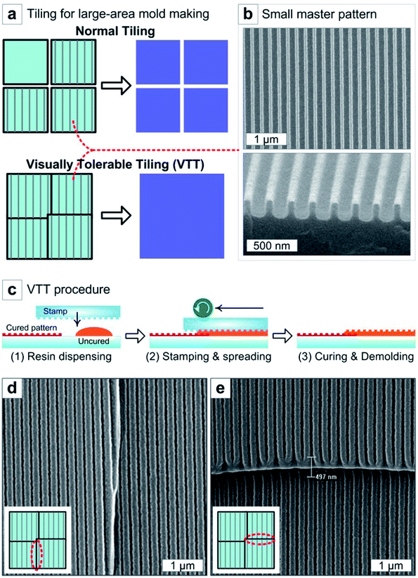 | ||
| Fig. 1 (a) Comparison schematic illustrations of normal tiling and overlapped tiling with a small master mold. (b) SEM image of a used master mold in the tiling process. (c) Schematics for the VTT process. (d) SEM image of the vertical seam part of nano-WGP patterns. (e) SEM image of the horizontal seam part of nano-WGP patterns. | ||
To overcome these problems, the proposed VTT process mold each tiles with slightly overlapped positioning. As a VTT resin, UV-curable polyurethaneacrylate (PUA) is used. A step-wise VTT procedure is illustrated in Fig. 1c. The uncured PUA pre-polymer is first dispensed next to the already cured PUA pattern and is covered with a master stamp facing down. For easier control and monitoring of the spreading of the pre-polymer underneath, the master stamp is preferably made of a transparent and compliant polymer film such as polyethylene terephthalate (PET). In VTT, the drop amount is roughly controlled to be less than what is needed to cover the entire surface of a master stamp, and the master stamp is positioned such that the projection of the master pattern area overlaps the previously replicated PUA pattern on the substrate (see (2) in Fig. 1c). Next by mechanically rolling the backside of a master stamp, the PUA pre-polymer spreads out until it touches the border of the pre-defined pattern area. It is noted that very precise control of the pre-polymer drop amount and stamp position is not necessary in VTT as long as the spread of the pre-polymer stays within the pattern area of the master stamp. Then the PUA pattern is cured by UV illumination followed by demolding of the master stamp. Fig. 1d and e show well-stitched PUA patterns fabricated by performing the VTT process using a PET master stamp of 200 nm-period nanograting pattern (shown in Fig. 1b). Watts et al. reported that the seam width needs to be narrower than 500 nm to be undetectable by the naked eye from their reports.11 In both the directions of parallel (Fig. 1c) and perpendicular (Fig. 1d) to grating patterns, seams span less than 500 nm which is smaller than what can be perceived by the naked eye because of the negligible change in optical transmission in the visible wavelength regime. Here, seams do not mean the overlapped region between the two prints, but refers to the discontinuous region between the former patterned area and the overlapped patterned area. For visible tolerance, therefore, the height between formal and latter patterns needs to be smaller than 500 nm and also, the spread width of the overlapped region needs to be narrower than 500 nm. This subwavelength nanoscale grating pattern with invisible seams is ideally suited to the large-area display components such as WGP films, which will be experimentally demonstrated later.
For easier examination of VTT-generated seams which may provide insights to understand the successful VTT mechanism, we now employ the microscale prism pattern array having 25 μm periods and 15 μm heights as an example. To investigate the seam formation in a generalized direction (not limited in parallel and perpendicular directions with respect to grating), we purposely perform VTT of the micro-prism pattern along an oblique direction using PUA resin. Fig. 2a shows such a VTT result of the micro-prism pattern with a clean, barely visible seam line. The inset in Fig. 2a reveals a vertical step between the two tiled zones, which is as small as 500 nm and thus may not change appreciably the optical transmission, and therefore cannot be perceived by the naked eye.
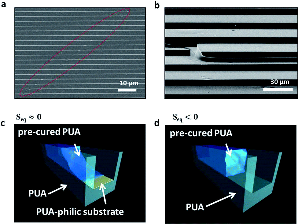 | ||
| Fig. 2 (a) SEM image of the seam part of micro-prism patterns. (b) SEM image of step on the overlapped micro-gratings along the seam line. (c) Illustrations of complete wetting conditions with almost zero value of spreading coefficient. (d) Illustrations of partial wetting conditions with negative spreading coefficient. | ||
In VTT, the dewetting characteristic of the uncured pre-polymer over the cured pattern is crucial to prevent the overflow onto the neighbored patterns. This wetting-mediated mechanism of successful VTT is easier to understand when imagining the opposite case; imagine the spacing between two neighboring grating lines fabricated from the anterior stamping and curing as the fluidic channel (Fig. 2c and d). Here we introduce an equilibrium spreading coefficient term, (Seq = γSV − γSL − γLV),12,13 which dictates whether a certain liquid will spread on the targeted surface or not. By Young's equation, γLV![[thin space (1/6-em)]](https://www.rsc.org/images/entities/char_2009.gif) cosθY = γSV − γSL, the equilibrium spreading coefficient can also be expressed with Seq = γLV(cosθY − 1). Here Seq indicates the wetting behavior of the liquid on specific surroundings. Seq is positive or almost zero for complete wetting, while a negative Seq represents rupturing and dewetting of the liquid thin film. The negative Seq allows partial wetting only and the film does not spread. Now when we drop an uncured pre-polymer on top, the infiltrated pre-polymer will form a meniscus in these lateral channels. If this meniscus is concave (i.e., Seq of the uncured pre-polymer with respect to the cured polymer channel is almost zero) as schematically illustrated in Fig. 2c, the pre-polymer will flow along the channels by capillary force, filling the nanochannels between the grating ridges. This will ruin the invisible tiling because the seam will essentially become a flat, unpatterned region. Fortunately, the uncured PUA has a negative Seq on the cured PUA surface because it contains acrylated organo-modified polysiloxanes as a releasing agent for self-replication.14 Consequently, the meniscus of uncured PUA inside the microchannel of cured PUA has almost a vertical profile (Fig. 2d) which effectively suppresses the channel filling of uncured resin until it is cured. This vertical step profile is experimentally confirmed by SEM imaging as shown in Fig. 2b.
cosθY = γSV − γSL, the equilibrium spreading coefficient can also be expressed with Seq = γLV(cosθY − 1). Here Seq indicates the wetting behavior of the liquid on specific surroundings. Seq is positive or almost zero for complete wetting, while a negative Seq represents rupturing and dewetting of the liquid thin film. The negative Seq allows partial wetting only and the film does not spread. Now when we drop an uncured pre-polymer on top, the infiltrated pre-polymer will form a meniscus in these lateral channels. If this meniscus is concave (i.e., Seq of the uncured pre-polymer with respect to the cured polymer channel is almost zero) as schematically illustrated in Fig. 2c, the pre-polymer will flow along the channels by capillary force, filling the nanochannels between the grating ridges. This will ruin the invisible tiling because the seam will essentially become a flat, unpatterned region. Fortunately, the uncured PUA has a negative Seq on the cured PUA surface because it contains acrylated organo-modified polysiloxanes as a releasing agent for self-replication.14 Consequently, the meniscus of uncured PUA inside the microchannel of cured PUA has almost a vertical profile (Fig. 2d) which effectively suppresses the channel filling of uncured resin until it is cured. This vertical step profile is experimentally confirmed by SEM imaging as shown in Fig. 2b.
The intrinsic dewetting properties (i.e., negative Seq) of uncured PUA drops on the cured PUA pattern require a certain level of normal force for the conformal spreading of the pre-polymer over the cured surface, which is achieved by mechanical rolling applied as schematically depicted in Fig. 1c. This is analogous to R2R NIL which enables the continuous patterning of polymer resin on either flexible or rigid substrates under a conformal contact. Here we use a flexible PET film for the VTT substrate. Since PUA is a self-replicable material, the flexible PUA/PET mold scaled up by VTT can serve as a R2R NIL mold for continuously churning out an even larger-area replica using PUA resin.
Fig. 3a schematically describes the step-wise VTT procedure, from initial tiling to the final R2R-based large-scale fabrication. By performing R2R NIL by wrapping the VTT-expanded flexible micro-prism pattern mold around a roll, a 1000 mm long and 120 mm wide prism sheet could be continuously produced with no visible seams (Fig. 3b). Likewise using the nanograting pattern presented in Fig. 1, a large-area PUA nanograting pattern mold can be made by VTT and then is applied in R2R NIL. In our present work, we repeat the tiling job eight times as a proof of concept; a 0.75 × 1 in. original stamp is used to produce a large R2R NIL stamp with dimensions of 4 × 6 in. The R2R-replicated nanograting pattern having a 220 nm period with a 180 nm height and 150 nm spacing (Fig. 3c) can be utilized in MWGP by shadow-evaporating Al on nanograting walls in an oblique angle (Fig. 3d).10 The process was developed to relax the requirement on nanoscale patterning of high aspect ratio and dense nanogratings. Especially targeting optical MWGP applications, the grating alignment between each mold tiling job is very important because a misalignment of wire grids may result in non-uniform color variation in MWGPs at different viewing angles.
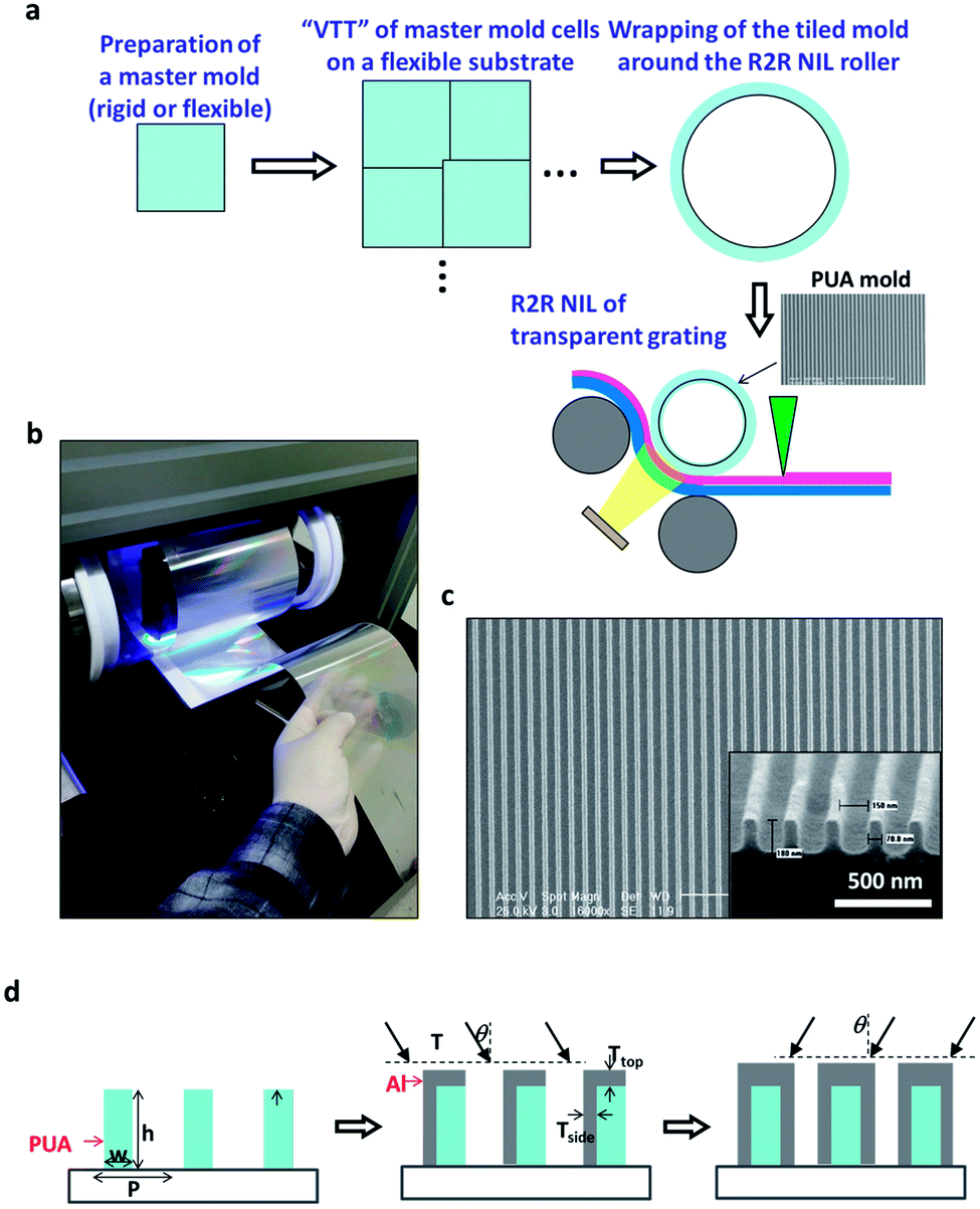 | ||
| Fig. 3 (a) Scheme of the roll to roll imprinting process by using a quasi-seamless mold. (b) Photograph of the R2R NIL process using a fabricated large area flexible mold. (c) Used nanogratings for the fabrication of the MWGP. (d) Schematic illustration of the double side shadow deposition process for WGP fabrication. | ||
Prior to actual fabrication, the as-imprinted nanograting and its Al-deposited structure are analyzed and optimized for MWGP applications through a set of G-Solver simulations. Based on the designed nanograting geometry (Fig. 3c), we choose a shadow deposition angle of 40° that can cover the entire sidewalls (i.e., arctan(150/180) ∼40°). The simulation results of polarizing performance for single-side and double-side shadow deposition cases can be found in the ESI (Fig. S1†). To find the optimal Al thickness, simulation is done with three different Al deposition thicknesses (i.e., 25, 50, and 75 nm). These simulation plots of transverse magnetic (TM) and transverse electric (TE) modes indicate that the designed Al/PUA architecture is acceptable for MWGP structures and the double-side deposition is more favorable for better extinction ratio (i.e., TM/TE). The dips in transmission mainly originate from the Fabry–Perot resonance which can be alleviated by controlling the aspect ratio and duty cycle (i.e., the ratio of grating line width to spacing) of metal grating.10
With the baseline understandings from simulation, we fabricate and characterize the MWGPs with the main focus on metal thickness control. Both glass and PET are used as substrates. To optimize the performance, the thickness of Al deposition varies to three values: 30 nm, 50 nm, and 70 nm. For the double-side deposition, we conduct two Al deposition runs with identical thicknesses, e.g., 30/30 nm, 50/50 nm, 70/70 nm. Fig. S2 and S3† present SEM images and performance data of single-side and double-side Al deposited MWGPs, respectively. We first confirm that MWGPs with only single-side Al deposition show a poor extinction ratio and undesirable dips, regardless of the Al thickness and substrate type (Fig. S2d–f†). This is because the metal grid period (i.e., 220 nm in the single-deposition case) is not sufficiently small to block the TE light, which can be improved by reducing the effective metal grid period through a method such as double-side deposition.10
The MWGPs fabricated by double-side Al deposition show much more improved performance (Fig. S3d–f†). As the Al thickness increases, the extinction ratio increases (up to 1000 in our case) since the decrease rate of TE transmittance is usually more influential than that of TM transmittance in mathematical calculation of the extinction ratio. As shown in Fig. 4, however, we observe a fair polarizing performance in the 30/30 nm thickness as well, with overall high TM transmittance (∼80%) which is generally desired in display panels. Additionally to improve MWGP performance, the metal etching process can also be incorporated, which removes metal layers from the top of the polymer pattern for higher and more uniform transmittance.10
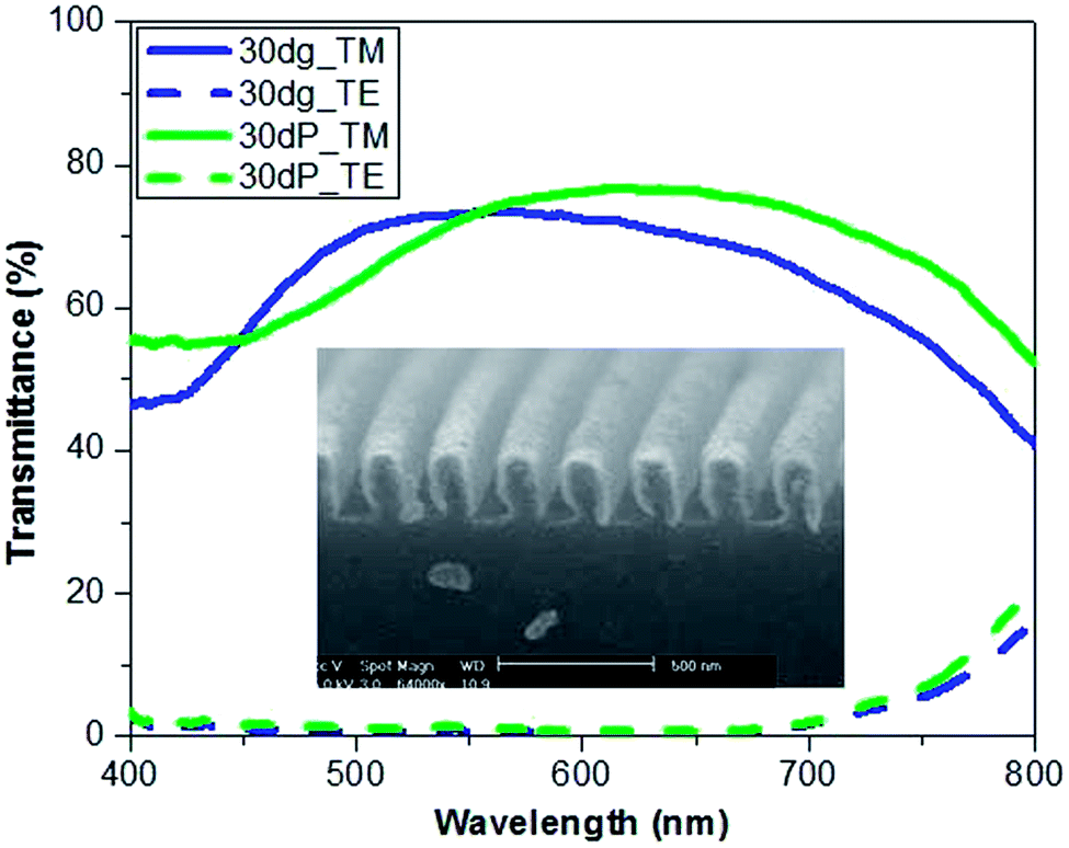 | ||
| Fig. 4 Cross-sectional SEM images and performance data of the 30 + 30 nm double side deposited wire grid polarizer. | ||
Now we turn to the VTT-based large-area MWGPs. As aforementioned, the size of the original master was 0.75 in × 1 in and the final sample size was 4 × 6 in by overlapped tiling. Fig. 5a is the photograph of normal nano-imprinted MWGPs as big as the original master area, and Fig. 5b shows the image of large area MWGPs fabricated by the R2R NIL using a VTT mold. The stitching lines are hardly visible to the naked eye for both TM and TE polarized light, while the entire fabrication protocol is not yet fully refined, we believe the large-area MWGPs could be practically fabricated with invisible seams via the VTT technique, without relying on other time-taking and costly methods. For another application, micro-prism sheets, the photo image of the fabricated sample is shown in Fig. S4.†
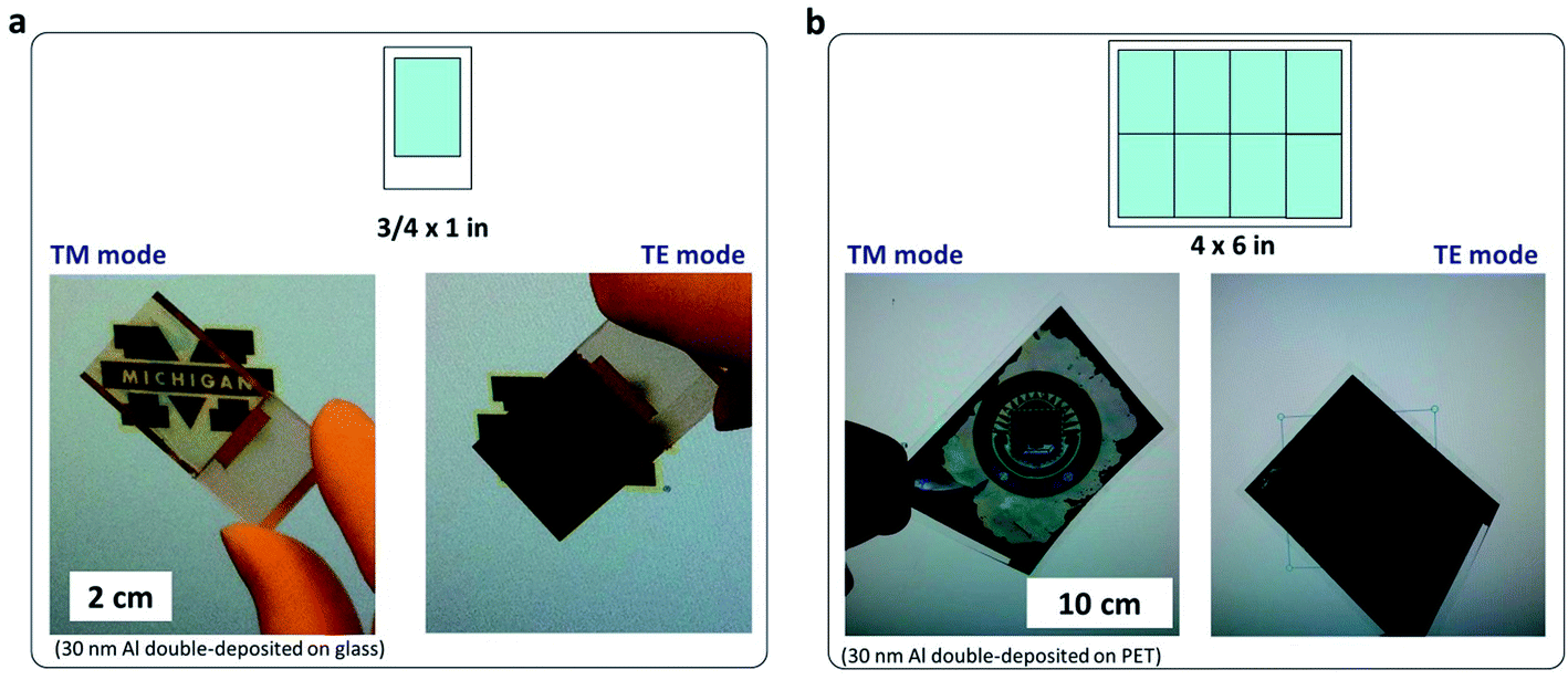 | ||
| Fig. 5 (a) Photo images of TE and TM modes of the fabricated wire grid polarizer with original master size. (b) TE and TM mode images of the large area wire grid polarizer which was fabricated by VTT. Large area sample was made by eight times overlapped patterning. All samples in (a) and (b) were fabricated by 30 + 30 nm double side deposition. | ||
Conclusions
In conclusion, we present a Visually Tolerable Tiling (VTT) methodology that enables the large-area scaling up of small-area micro/nano-scale pattern molds without perceivable seam lines. The key to successful VTT is to perform slightly overlapped stamping of small pattern tiles using the self-replicable and dewetting resin under sufficient pressure. The seams are successfully suppressed within 500 nm width and thus are not perceivable by the naked eye. While the VTT-expanded quasi-seamless MWGPs are demonstrated as a proof of concept, we envision this VTT strategy could be further utilized in various large-area optical and display devices.Methods
Materials
UV-curable polyurethane functionalized with acrylate groups (PUA) was kindly provided by Minuta Tech. (Product name: MINS-301 RM, Korea). PUA pre-polymer has a cycloaliphatic and linear long chain. Therefore, the fabricated PUA mold is rigid enough to produce fine features (down to a few hundred nanometers) but also flexible on the film support. This characteristic was named “rigiflex (rigid + flexible) mold”.14Tiling process for visually tolerable large-area patterns
The glass and PET films used in this study were coated with a surface modification primer of urethane groups to increase adhesion to the acrylate-containing monomer. An adequate amount of a UV curable PUA pre-polymer was drop-dispensed on the primer-coated glass or PET film, and a small pattern master stamp was carefully placed on top of the surface to make conformal contact. The sample was then exposed to UV light to cure the PUA pre-polymer (Linear UV LED equipment with 365 nm wavelength, UVSMT, at an intensity of 100 mW cm−2). After the first replication, the second replication was performed next to the first cured PUA pattern. The pre-polymer was drop-dispensed and was carefully spread within the master pattern region by mechanical rolling, until the spread reaches and overlaps slightly with respect to the already formed patterns.Acknowledgements
MKK acknowledges the support by a grant from the Young Researchers Supporting Program through the National Research Foundation of Korea (NRF) funded by the Ministry of Education, Science and Technology (2012R1A1A1040040) and Global Excellent Technology Innovation (10045070), Small and Medium Business Administration (S2098429) funded by the Ministry of Trade, Industry&Energy(MOTIE)/KEIT of Korea. JGO and LJG acknowledge the support by NSF CMMI 1025020, a subcontract from UMass' CHM center.References
- S. H. Ahn and L. J. Guo, Adv. Mater., 2008, 20, 2044–2049 CrossRef CAS.
- S. H. Ahn and L. J. Guo, ACS Nano, 2009, 3, 2304–2310 CrossRef CAS PubMed.
- Y.-F. Huang, S. Chattopadhyay, Y.-J. Jen, C.-Y. Peng, T.-A. Liu, Y.-K. Hsu, C.-L. Pan, H.-C. Lo, C.-H. Hsu, Y.-H. Chang, C.-S. Lee, K.-H. Chen and L.-C. Chen, Nat. Nanotechnol., 2007, 2, 770–774 CrossRef CAS PubMed.
- F. C. Krebs, T. Tromholt and M. Jorgensen, Nanoscale, 2010, 2, 873–886 RSC.
- M. K. Kwak, T.-i. Kim, P. Kim, H. H. Lee and K. Y. Suh, Small, 2009, 5, 928–932 CrossRef CAS PubMed.
- G. R. Bird and J. M. Parrish, J. Opt. Soc. Am., 1960, 50, 886 CrossRef.
- E. Hecht, Optics, Addison-Wesley, Texas, 4th edn, 2002 Search PubMed.
- S. H. Ahn, J.-S. Kim and L. J. Guo, J. Vac. Sci. Technol., B: Microelectron. Nanometer Struct.–Process., Meas., Phenom., 2007, 25, 2388–2391 CrossRef CAS.
- S.-W. Ahn, K.-D. Lee, J.-S. Kim, S. H. Kim, J.-D. Park, S.-H. Lee and P.-W. Yoon, Nanotechnology, 2005, 16, 1874 CrossRef CAS.
- Y. J. Shin, P.-H. Carlos, Y.-K. Wu, J. G. Ok and L. J. Guo, Nanotechnology, 2012, 23, 344018 CrossRef PubMed.
- M. P. C. Watts, M. Little, E. Egan, A. Hochbaum, C. Johns and S. Stephansen, A Process for and Properties of Low Cost Wire Grid Polarizers, http://www.impattern.com/files/WGPImpattern2.0.pdf, accessed: 11, 2013 Search PubMed.
- P. Kim, H.-Y. Kim, J. K. Kim, G. Reiter and K. Y. Suh, Lab Chip, 2009, 9, 3255–3260 RSC.
- S. Wu, Polymer Interface and Adhesion, Dekker, New York, 1982 Search PubMed.
- S.-J. Choi, H. N. Kim, W. G. Bae and K.-Y. Suh, J. Mater. Chem., 2011, 21, 14325–14335 RSC.
Footnotes |
| † Electronic supplementary information (ESI) available. See DOI: 10.1039/c4mh00159a |
| ‡ These authors contributed equally to this study. |
| This journal is © The Royal Society of Chemistry 2015 |