
 Open Access Article
 This Open Access Article is licensed under a Creative Commons Attribution-Non Commercial 3.0 Unported Licence
Site-specific nanopatterning of functional metallic and molecular arbitrary features in nanofluidic channels†
Yan
Xu
*a,
Nobuhiro
Matsumoto
ab,
Qian
Wu
ac,
Yuji
Shimatani
ac and
Hiroaki
Kawata
b
aNanoscience and Nanotechnology Research Center, Research Organization for the 21st Century, Osaka Prefecture University, 1-2, Gakuen-cho, Naka-ku, Sakai, Osaka 599-8570, Japan. E-mail: y-xu@21c.osakafu-u.ac.jp
bDepartment of Physics and Electronics, Graduate School of Engineering, Osaka Prefecture University, 1-1, Gakuen-cho, Naka-ku, Sakai, Osaka 599-8531, Japan
cDepartment of Chemistry, Graduate School of Science, Osaka Prefecture University, 1-1, Gakuen-cho, Naka-ku, Sakai, Osaka 599-8531, Japan
First published on 9th March 2015
Abstract
We established a versatile method for site-specific nanopatterning of functional metallic and molecular arbitrary features in glass nanofluidic channels, with well-controlled feature sizes ranging from tens to hundreds of nanometers and precisely controlled placements in the range of several tens of nanometers. With the method, we achieved the fabrication of quasi-0D, quasi-1D, 2D, and 3D gold nanopatterns in nanofluidic channels, as well as a high-density fluorescent molecular nanoarray in arrayed femtoliter nanofluidic channels. The method opens the way for precise functionalization of nanofluidic channels, which has been greatly challenging in the field of nanofluidics.
Nanofluidics, the study of fluids in channels with nanometer-scale dimensions, is a potential solution to a variety of challenges in areas of separation, sensing, and detection of molecules at the single-molecule level.1–3 Nanofluidics is also promising because it provides tools for elucidation of transport phenomena, chemical reactions, biological processes, and life phenomena confined in nanoscale spaces.4–7 Nevertheless, in contrast to its thriving ‘brother’ microfluidics, nanofluidics is still a nascent field. The lack of methods for the functionalization of nanofluidic channels is one of the most critical bottlenecks for promoting both fundamental and applied research on nanofluidics.
The functionalization of nanofluidic channels is challenging. For open planar systems, many physical, chemical, and mechanical methods have been developed to functionalize the systems at zero, one, two or three dimensions in the nanometer range.8–14 Unfortunately, for small closed space systems like nanofluidic channels, most of these methods face obstacles in either principles or practices due to the physical barrier resulting from the ‘closed’ feature of these systems.
As the space size decreases to the micro-/nanometer scale, the surface-area-to-volume ratio increases significantly. As a result, the properties of the internal surface of a small closed space dominate a variety of phenomena and processes in the space. Hence, fabrication, modification, and control of the local internal surface are indispensable strategies for the functionalization of small closed space systems. Surface patterning is a basic way to fabricate, modify, and control the properties of the local surface of a material. In the field of microfluidics, photo-patterning (Fig. S1 in the ESI†) is a predominant method to pattern the internal surface of a closed microfluidic channel,15–18 in addition to few other patterning methods.19,20 On the one hand, the method takes advantage of the nature of light (commonly, UV light), as light can pass through the transparent physical barrier of the substrate layer and thereby enables patterning of various photo-reactive materials on the internal surface of the “closed” microfluidic channel, using a photomask. On the other hand, the patterning capability of the method is restricted by the nature of light, namely, the diffraction limit, as well as the resolution limit of the photomask and other instrumental limitations. Consequently, the feature sizes and the placement precision of the pattern are generally in the micrometer range and practically difficult to be further downscaled to the nanometer range. Obviously, nanopatterning of the internal surfaces of nanofluidic channels exceeds the capability of photo-patterning. Therefore, in order to accelerate and broaden the research on nanofluidics, methods capable of nanopatterning in nanofluidic channels should be established.
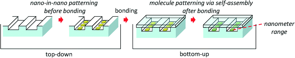
Unlike the patterning-after-bonding strategy of the photo-patterning in microfluidics (Fig. S1, in the ESI†), in this study a different general methodology (Fig. 1) was proposed to achieve nanopatterning in nanofluidic channels. The method comprises primary nano-in-nano patterning before bonding by utilizing top-down approaches and secondary molecule patterning after bonding by utilizing bottom-up approaches. The method does not use UV light, and therefore the capability of patterning is not restricted by the diffraction limit of light and the resolution limit of the photomask. The method enables the site-specific fabrication of a variety of nanopatterns with arbitrary shapes and sizes in single nanofluidic channels, nanofluidic channel networks, and arrayed nanofluidic channels. Not only metallic but also molecular nanopatterns and nanoarrays can be formed in nanofluidic channels by utilizing the method.
 | ||
| Fig. 1 Schematic drawing of nanopatterning in nanofluidic channels. | ||
In brief, the method (Fig. 1) is described as follows. First, gold is pre-nanopatterned in open nanofluidic channels utilizing top-down processes of electron beam (EB) lithography, deposition, and lift-off which are guided by a high-precision placement control technique. Then, the gold-nanopatterned open nanofluidic channels are bonded without damage utilizing a gold-pattern-friendly bonding technique to form closed nanofluidic channels. Next, a solution of functional molecules bearing thiol or disulfide groups is introduced into the nanofluidic channels. Consequently, a functional molecular nanopattern specifically forms on the surface of the gold nanopatterns in the nanofluidic channels by bottom-up molecular self-assembly, owing to well-known thiol–gold or disulfide–gold interactions.21,22
The method includes two key techniques to surmount two hurdles in the establishment of the novel patterning method, described as follows.
One hurdle was how to precisely pattern gold in open nanofluidic channels. As 3D hierarchical nanostructures formed by dissimilar materials, open glass nanofluidic channels with gold nanopatterns cannot be fabricated by a one-step process utilizing current available nanofabrication approaches. Therefore, a two-step process consisting of (i) nanofabrication of nanofluidic channels followed by (ii) gold nano-deposition on exact locations in the open nanofluidic channels in a controlled manner (i.e., nano-in-nano patterning; Fig. S2a and b in the ESI†) is unavoidable but is greatly challenging.
This hurdle was surmounted by a placement control technique with super high precision. The technique was based on accurate positioning of the fabrication placement assisted by a pair of gold reference marks pre-fabricated on the substrate. The gold reference marks could be searched manually and recognized by using a backscatter detector of an EB system when being scanned with the electron beam, according to a backscattered electron yield different from that of the glass substrate. The rotational deviation and the positional deviation during substrate mounting were thereby detected, calculated with respect to the actual position, and offset by driving an X–Y stage of the EB system. As a result, the relative positional relationship between the reference marks on computer-aided design (CAD) data and those on the actual sample could be finally matched, which enabled superposition drawing with high precision during multiple-step nanofabrication using the EB system. Reference marks with different shapes and sizes were tested. Symmetrical cross-marks of gold/chromium (Au/Cr, 100 nm/5 nm thick) with several tens of nanometers in width and several hundreds of nanometers in length were utilized in this study, based on the fabrication capability and reproducibility of our fabrication facilities. By using the reference marks, a placement control with super high precision of several tens of nanometers in both X-axis and Y-axis directions was achieved, as indicated in Fig. S3 in the ESI.† For example, the super high-precision placement control enabled the site-specific fabrication of a very challenging nanopattern whose one side (Fig. 2c) or both upper and lower sides (Fig. 2d, h) is exactly located at the edges of the bottom of the nanofluidic channels (800 nm wide and 300 nm deep), without any protrusion of gold to the outside of the nanofluidic channels. Moreover, the fabricated gold reference marks were quite robust even after experiencing EB lithography (EBL), dry etching, and various harsh liquid processes of pattern development, metal lift-off, and substrate cleaning several times. The gold reference marks could work efficiently for nanofabrication with more than two steps, practically. For example, Fig. 2j shows a scanning electron microscope (SEM) image of a gold-bottomed nanowell array in arrayed nanofluidic channels. The structure is a nano-in-nano-in-nano structure, which was fabricated by three-step nanofabrication (Fig. 2j, according to a process described in Fig. S2c and d in the ESI†).
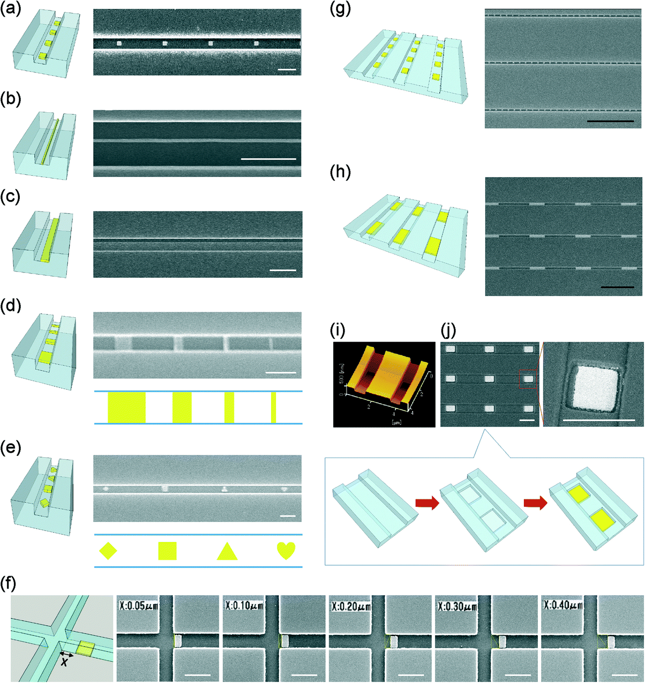 | ||
| Fig. 2 Schematic and SEM images of gold nanopatterns with arbitrary structures fabricated in (a–e) single nanofluidic channels, (f) nanofluidic channel networks, and (g, h, and j) arrayed nanofluidic channels. (a) Nanodots; (b) nanowires; (c) nanostripes; (d) gradient nanopatterns; (e) diamond, square, triangle, and heart-shaped nanopatterns; (f) rectangular nanopatterns in cross-shaped nanofluidic channel networks with varying X distances (50 nm, 100 nm, 200 nm, 300 nm, and 400 nm) which are defined in the corresponding schematic image; (g) a nanodot array in arrayed nanofluidic channels; (h) a full-width nanosegment array in arrayed nanofluidic channels; (i) a nanowell array (AFM image) and (j) a gold-bottomed nanowell array in arrayed nanofluidic channels. White scale bar is 1 μm and black scale bar is 10 μm. | ||
Another hurdle was how to bond gold-patterned nanofluidic channels without destroying the pre-patterned gold. While there are several substrate materials such as glass, polydimethylsiloxane (PDMS), and plastics to choose in the fabrication of microfluidic chips, glass (here referring specifically to fused-silica which is glass consisting of silica in the amorphous form) is currently almost the sole ideal substrate material in the fabrication of nanofluidic chips. This is owing to its chemical and mechanical stability, superior optical and thermal properties, and well-established nanofabrication technologies. In standard practice, nanofluidic chips are fabricated by fusion bonding of upper and lower glass substrates containing micro-/nanofluidic channels and other structures.23 However, the glass fusion bonding is required to be performed under vacuum at over 1000 °C, which is near the melting point of gold under atmospheric pressure. The ultra-high temperature would inevitably lead to damage of the gold patterns.
Gold-pattern-friendly bonding of glass nanofluidic chips was developed to surmount the second hurdle. We have developed room temperature bonding of glass nanofluidic channels based on one-step surface activation using O2/CF4 plasma treatment.24 The O2/CF4 plasma treatment is suitable for bonding bare nanofluidic channels but is not friendly for bonding gold-nanopatterned nanofluidic channels. The problem is that etching and fluorination effects on the gold surface during the O2/CF4 plasma treatment could lead to damage of the gold, as reported elsewhere.25,26 To avoid this potential problem, in this study a different surface activation process using the O2 plasma without addition of CF4 was proposed. Briefly, first, the perfectly cleaned substrates were treated with the O2 plasma for 15 min, two times, at a power of 200 W and a flow rate of 100 mL min−1. After that, the substrates were preliminarily bonded by being in contact with each other, with the use of hands, at room temperature, followed by thermal bonding under vacuum. The process allowed the gold-nanopatterned nanofluidic channels to bond under vacuum conditions of several 100 Pa, at 600 °C. Most importantly, the gold patterns survived after bonding and no damage was observed (Fig. 3d). The results should be owing to the fact that the bonding temperature was much below the melting point of gold. Moreover, the bonded nanofluidic chip could work continuously without leakage during liquid introduction driven by air pressure (Fig. 3e), even at 430 kPa for six days (Fig. S4 in the ESI†). This pressure range can meet the requirements of most nanofluidic operations. Furthermore, as shown in Fig. 3f and g, the gold nanopatterns (Fig. 3d) in the bonded nanofluidic chips (Fig. 3a, b) kept their ability to interact with disulfides to form SAM on the nanometer scale. This result suggests that the bonding did not bring about adverse influence which could lead to failure in the formation of self-assembled monolayers (SAM) on the gold surface.
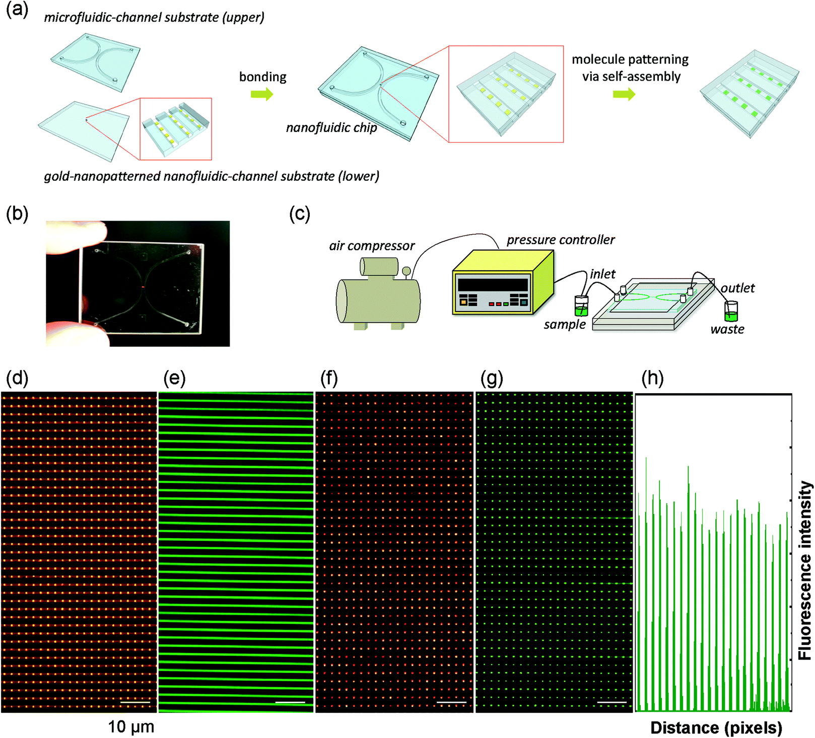 | ||
| Fig. 3 (a) Formation of the fluorescent molecular nanoarray in gold-nanopatterned nanofluidic channels of (b) a chip by introducing a fluorescein disulfide solution with (c) an air pressure-based liquid introduction system. (d) A bright-field image of the gold-nanopatterned nanofluidic channels before the liquid introduction and (e) a fluorescence image of the channels after continuous liquid introduction for 2 h. (f) A bright-field image and (g) a fluorescence image of the formed fluorescent molecular nanoarray, with (h) a profile of fluorescence intensity of the first row of (g). | ||
The nanopatterning supported by the above-described two key techniques enabled site-specific fabrication of gold nanopatterns in glass nanofluidic channels, with actual dimensions approximately the same as the targeted dimensions. Fig. 2 shows the SEM or atomic force microscope (AFM) images of nanodots (290 nm; Fig. 2a), nanowires (66 nm wide; Fig. 2b), nanostripes (570 nm wide; Fig. 2c), and nanowells (700 nm square and 200 nm deep; Fig. 2i) with gold bottoms (600 nm square; Fig. 2j) fabricated in nanofluidic channels (800 nm wide and 300 nm deep), representing quasi-0D, quasi-1D, 2D and 3D nanopatterns, respectively. These reproducible nanostructures had feature sizes ranging from tens to hundreds of nanometers. These nanostructures are typical structures widely used in a variety of systems in nanoscience and nanotechnology, but were fabricated for the first time in nanofluidic channels. Multiple patterns with arbitrary shapes in a single nanofluidic channel were also achieved. For example, while Fig. 2d shows the SEM image of a series of gold patterns with various gradient lengths (890 nm, 520 nm, 330 nm, and 160 nm) in a single nanofluidic channel (800 nm wide and 300 nm deep), Fig. 2e demonstrates the SEM image of diamond, square, triangle, and heart-shaped gold nanopatterns in a single nanofluidic channel (680 nm wide and 300 nm deep). Moreover, the ability of site specificity was further demonstrated by fabrication of a nanometer-level-positioning-required structure in a cross-shaped nanofluidic channel (520 nm wide and 240 nm deep), as shown in Fig. 2f. The rectangular gold nanopattern (300 nm × 470 nm) positioned at a specified distance (for example, 50 nm, 100 nm, 200 nm, 300 nm, and 400 nm) with respect to the boundary of a branch of the nanofluidic channel network was precisely fabricated as desired. In addition, these nanopatterns could be fabricated as nanoarrays in arrayed nanofluidic channels, as shown in Fig. 2g, h, and j.
A self-assembled molecular nanoarray in arrayed nanofluidic channels was achieved in a nanofluidic chip by utilizing the nanopatterning method (Fig. 3a, b). The nanofluidic chip contains a micro-/nanofluidic channel hybrid, which is a standard chip structure used in nanofluidics to facilitate liquid handling in nanofluidic channels.24,27–29 In the chip, two side microfluidic channels (3 μm deep and 500 μm wide) are bridged by 100 parallel-arrayed nanofluidic channels (300 nm deep, 800 nm wide, and 400 μm long, spaced by 2 μm), with a gold nanoarray (500 nm square, spaced by 2 μm) in each nanofluidic channel. The structure provides a 160 × 100 (= 16![[thin space (1/6-em)]](https://www.rsc.org/images/entities/char_2009.gif) 000) nanodot-shaped gold array on an area of 400 μm × 280 μm (= 0.112 mm2) in the chip, as partially shown in Fig. 3d. Each nanofluidic channel has an ultra-small volume of approximately 96 fL (femtoliter (fL) = 10−15 L). Thus, the arrayed nanofluidic channels are appropriately to handle 9.6 pL (picoliter, pL = 10−12 L) of liquid, which is the same as the volume of a single mammalian cell. All liquids were introduced to the arrayed nanofluidic channels through the microfluidic channels by air pressure which was regulated using a 0.1 kPa resolved pressure control system (Fig. 3c). An ethanol solution of HOOC–(CH2)10–S–S–(CH2)10–CONH–fluorescein was introduced (Fig. 3e) to form the molecular nanoarray by molecular self-assembly in the nanofluidic channels. HOOC–(CH2)10–S–S–(CH2)10–CONH–fluorescein is a fluorescein disulfide which can form SAM on the gold surface via disulfide–gold interactions. It is widely used to visualize the defects and ordering of the SAM structure, owing to its easily detectable fluorescence. A high-density nanoarray (160 × 100) of the fluorescein disulfide SAM was confirmed on the entire 400 μm × 280 μm tiny area of the arrayed nanofluidic channels by using a fluorescence microscope. Fig. 3f and g show a bright-field image and a corresponding fluorescence image of a part of the molecular nanoarray, respectively. Fig. 3h shows the profile of fluorescence intensity of the first row of the array shown in Fig. 3g. The nanodot-shaped fluorescent array (Fig. 3g) with a high resolution (Fig. 3h) indicates that the disulfide molecules were successfully self-assembled on the gold nanoarray in the nanofluidic channels. The fluorescence of the nanoarray remained detectable after continuous flowing of absolute ethanol by air pressure at 430 kPa, for 18 h. These results reveal that the molecular nanoarray was stable even under high-pressure fluidic conditions for a long term.
000) nanodot-shaped gold array on an area of 400 μm × 280 μm (= 0.112 mm2) in the chip, as partially shown in Fig. 3d. Each nanofluidic channel has an ultra-small volume of approximately 96 fL (femtoliter (fL) = 10−15 L). Thus, the arrayed nanofluidic channels are appropriately to handle 9.6 pL (picoliter, pL = 10−12 L) of liquid, which is the same as the volume of a single mammalian cell. All liquids were introduced to the arrayed nanofluidic channels through the microfluidic channels by air pressure which was regulated using a 0.1 kPa resolved pressure control system (Fig. 3c). An ethanol solution of HOOC–(CH2)10–S–S–(CH2)10–CONH–fluorescein was introduced (Fig. 3e) to form the molecular nanoarray by molecular self-assembly in the nanofluidic channels. HOOC–(CH2)10–S–S–(CH2)10–CONH–fluorescein is a fluorescein disulfide which can form SAM on the gold surface via disulfide–gold interactions. It is widely used to visualize the defects and ordering of the SAM structure, owing to its easily detectable fluorescence. A high-density nanoarray (160 × 100) of the fluorescein disulfide SAM was confirmed on the entire 400 μm × 280 μm tiny area of the arrayed nanofluidic channels by using a fluorescence microscope. Fig. 3f and g show a bright-field image and a corresponding fluorescence image of a part of the molecular nanoarray, respectively. Fig. 3h shows the profile of fluorescence intensity of the first row of the array shown in Fig. 3g. The nanodot-shaped fluorescent array (Fig. 3g) with a high resolution (Fig. 3h) indicates that the disulfide molecules were successfully self-assembled on the gold nanoarray in the nanofluidic channels. The fluorescence of the nanoarray remained detectable after continuous flowing of absolute ethanol by air pressure at 430 kPa, for 18 h. These results reveal that the molecular nanoarray was stable even under high-pressure fluidic conditions for a long term.
In conclusion, we established a versatile method enabling site-specific nanopatterning of metallic and molecular arbitrary features in glass nanofluidic channels, based on the proposed methodology comprising nano-in-nano patterning before bonding and molecule patterning after bonding. To achieve the method, we developed two key techniques, namely, the placement control with a precision of several tens of nanometers for multiple-step nanofabrication and the gold-pattern-friendly bonding of nanofluidic chips. With the nanopatterning supported by the two techniques, we achieved the fabrication of quasi-0D, quasi-1D, 2D, and 3D gold nanopatterns in nanofluidic channels as well as a high-density molecular array in arrayed femtoliter nanofluidic channels for the first time. These versatile nanopatterns are very promising because they can work as fluidic, electrical, optical, thermal, magnetic, chemical and biological functional units in nanofluidic chips after further design, characterization, optimization, and integration in the future. In the field of nanofluidics, due to the lack of methods for functionalization of nanofluidic channels, until now most studies have to stay at a level of investigation of phenomena confined in less controllable, bare nanofluidic channels. Therefore, we believe that nanopatterning will help accelerate and broaden both the fundamental and the applied research on nanofluidics.
Acknowledgements
This work was partially supported by JSPS KAKENHI (grant no. 26706010, 26630403), MEXT KAKENHI (grant no. 26107714), and the Asahi Glass Foundation.Notes and references
- C. A. Aguilar and H. G. Craighead, Nat. Nanotechnol., 2013, 8, 709–718 CrossRef CAS PubMed.
- L. D. Menard, C. E. Mair, M. E. Woodson, J. P. Alarie and J. M. Ramsey, ACS Nano, 2012, 6, 9087–9094 CrossRef CAS PubMed.
- Y. Xu, K. Jang, T. Yamashita, Y. Tanaka, K. Mawatari and T. Kitamori, Anal. Bioanal. Chem., 2012, 402, 99–107 CrossRef CAS PubMed.
- W. Sparreboom, A. van den Berg and J. C. T. Eijkel, Nat. Nanotechnol., 2009, 4, 713–720 CrossRef CAS PubMed.
- A. Piruska, M. Gong, J. V. Sweedler and P. W. Bohn, Chem. Soc. Rev., 2010, 39, 1060–1072 RSC.
- J. M. Perry, K. M. Zhou, Z. D. Harms and S. C. Jacobson, ACS Nano, 2010, 4, 3897–3902 CrossRef CAS PubMed.
- T. Yasui, N. Kaji, M. R. Mohamadi, Y. Okamoto, M. Tokeshi, Y. Horiike and Y. Baba, ACS Nano, 2011, 5, 7775–7780 CrossRef CAS PubMed.
- A. A. Tseng, K. Chen, C. D. Chen and K. J. Ma, IEEE Trans. Adv. Packag., 2003, 26, 141–149 CrossRef CAS.
- K. Ostrikov, Rev. Mod. Phys., 2005, 77, 489–511 CrossRef CAS.
- B. D. Gates, Q. B. Xu, M. Stewart, D. Ryan, C. G. Willson and G. M. Whitesides, Chem. Rev., 2005, 105, 1171–1196 CrossRef CAS PubMed.
- K. C. Park, H. J. Choi, C. H. Chang, R. E. Cohen, G. H. McKinley and G. Barbastathis, ACS Nano, 2012, 6, 3789–3799 CrossRef CAS PubMed.
- C. L. Haynes and R. P. Van Duyne, J. Phys. Chem. B, 2001, 105, 5599–5611 CrossRef CAS.
- G. M. Whitesides and B. Grzybowski, Science, 2002, 295, 2418–2421 CrossRef CAS PubMed.
- J. Chai and J. M. Buriak, ACS Nano, 2008, 2, 489–501 CrossRef CAS PubMed.
- C. Priest, Biomicrofluidics, 2010, 4, 032206 CrossRef PubMed.
- K. Jang, K. Sato, Y. Tanaka, Y. Xu, M. Sato, T. Nakajima, K. Mawatari, T. Konno, K. Ishihara and T. Kitamori, Lab Chip, 2010, 10, 1937–1945 RSC.
- S. W. Hu, X. Q. Ren, M. Bachman, C. E. Sims, G. P. Li and N. L. Allbritton, Anal. Chem., 2004, 76, 1865–1870 CrossRef CAS PubMed.
- M. A. Holden, S. Y. Jung and P. S. Cremer, Anal. Chem., 2004, 76, 1838–1843 CrossRef CAS PubMed.
- E. Delamarche, D. Juncker and H. Schmid, Adv. Mater., 2005, 17, 2911–2933 CrossRef CAS.
- P. J. A. Kenis, R. F. Ismagilov and G. M. Whitesides, Science, 1999, 285, 83–85 CrossRef CAS.
- J. C. Love, L. A. Estroff, J. K. Kriebel, R. G. Nuzzo and G. M. Whitesides, Chem. Rev., 2005, 105, 1103–1169 CrossRef CAS PubMed.
- D. Samanta and A. Sarkar, Chem. Soc. Rev., 2011, 40, 2567–2592 RSC.
- T. Tsukahara, K. Mawatari, A. Hibara and T. Kitamori, Anal. Bioanal. Chem., 2008, 391, 2745–2752 CrossRef CAS PubMed.
- Y. Xu, C. X. Wang, L. X. Li, N. Matsumoto, K. Jang, Y. Y. Dong, K. Mawatari, T. Suga and T. Kitamori, Lab Chip, 2013, 13, 1048–1052 RSC.
- Y. Taniguchi and T. Shin-mura, J. Vac. Sci. Technol., A, 1998, 16, 2042–2046 CAS.
- R. M. Ranade, S. S. Ang and W. D. Brown, J. Electrochem. Soc., 1993, 140, 3676–3678 CrossRef CAS PubMed.
- S. R. Liu, Q. S. Pu, L. Gao, C. Korzeniewski and C. Matzke, Nano Lett., 2005, 5, 1389–1393 CrossRef CAS.
- C. H. Duan and A. Majumdar, Nat. Nanotechnol., 2010, 5, 848–852 CrossRef CAS PubMed.
- Y. Xu, C. X. Wang, Y. Y. Dong, L. X. Li, K. Jang, K. Mawatari, T. Suga and T. Kitamori, Anal. Bioanal. Chem., 2012, 402, 1011–1018 CrossRef CAS PubMed.
Footnote |
| † Electronic supplementary information (ESI) available: Schematic drawing of photo-patterning widely used in microfluidics (Fig. S1†); nano-in-nano fabrication guided by the high-precision placement control technique (Fig. S2†); evaluation of precision of the placement control technique (Fig. S3†); long-term evaluation of the gold-pattern-friendly bonding under continuous nanofluidic conditions at a high pressure (Fig. S4 in the ESI†); and Experimental section. See DOI: 10.1039/c5lc00190k |
| This journal is © The Royal Society of Chemistry 2015 |