
 Open Access Article
 This Open Access Article is licensed under a
 Creative Commons Attribution 3.0 Unported Licence
Etching of glass microchips with supercritical water†
Pavel
Karásek
*,
Jakub
Grym
,
Michal
Roth
,
Josef
Planeta
and
František
Foret
Institute of Analytical Chemistry of the ASCR v. v. i., Veveri 97, 602 00, Brno, Czech Republic. E-mail: karasek@iach.cz; foret@iach.cz; Fax: +420 541 212 113; Tel: +420 532 290 175
First published on 24th October 2014
Abstract
A novel method of etching channels in glass microchips with the most tunable solvent, water, was tested as an alternative to common hydrogen fluoride-containing etchants. The etching properties of water strongly depend on temperature and pressure, especially in the vicinity of the water critical point. The chips were etched at the subcritical, supercritical and critical temperature of water, and the resulting channel shape, width, depth and surface morphology were studied by scanning electron microscopy and 3D laser profilometry. Channels etched with the hot water were compared with the chips etched with standard hydrogen fluoride-containing solution. Depending on the water pressure and temperature, the silicate dissolved from the glass could be re-deposited on the channel surface. This interesting phenomenon is described together with the conditions necessary for its utilization. The results illustrate the versatility of pure water as a glass etching and surface morphing agent.
Introduction
Photolithography and etching represent important operations in the majority of microfabrication processes.1 Although simpler procedures can be used for replication of microfluidic systems (e.g., PDMS casting, injection molding, etc.), a suitable master has to be fabricated first, often including the wet etching step. While there are many different etching protocols using solution or gas phase chemistries, hydrogen fluoride etching is the most common procedure for glass or fused silica substrates. Water is commonly used as a solvent for the etching solution and for subsequent washing steps since it is inert at atmospheric pressure and ambient temperature.In chemical extractions and reactions, water takes a prominent position among the sustainable alternatives to organic solvents because it is the most tunable solvent in terms of shifts in the solvent properties that may result from variations in the operating temperature and pressure.2 However, the applications of water as a solvent or reaction agent under the conditions near and above its vapor–liquid critical point (tc = 373.95 °C, Pc = 22.064 MPa) are not restricted only to the domain of organic substances. From geology it is known that most materials (including glass), commonly considered as insoluble, do dissolve in water, albeit at a very slow rate. The rate of dissolution can be orders of magnitude faster at elevated pressures and temperatures as documented in geology. More recently such geologic processes have been studied quantitatively in the laboratory showing granite–distilled water interactions at temperatures and pressures up to 180 °C and 1.4 MPa.3 Supercritical water (SCW) has been known to dissolve both quartz4 and fused silica5 and plays an important role in the transport and crystallization of siliceous minerals.6 We have previously shown that supercritical water is a versatile agent to manipulate the internal diameter and the inner surface roughness of fused silica capillaries.7–9
Since the high-temperature water can dissolve quartz and fused silica (non-ionic substances), it can be expected to dissolve (ionic substances) glass, even under milder temperature and pressure conditions. In the present work, we describe the initial study of high-temperature water etching of microchannel structures in glass substrates and compare the results with the standard, hydrogen fluoride-containing etching mixture.
Experimental section
Materials and chemicals
Commercial 40 mm × 40 mm borosilicate glass substrates (Borofloat, 60% SiO2, 15% Al2O3, 5% B2O3) coated with a low reflective chromium layer and AZ1518 + AZTFP650 photoresist coating were purchased from Nanofilm, Westlake Village, CA, USA. Hydrofluoric acid, ammonium fluoride and hydrochloric acid were purchased from Sigma-Aldrich spol. s.r.o., Prague, Czech Republic. Water pretreatment included double distillation followed by purification with reverse osmosis (Ultra Clear UV, SG Wasseraufbereitung und Regenerierstation GmbH, Barsbüttel, Germany). Before entering the apparatus, water was thoroughly stripped of the dissolved oxygen and carbon dioxide by bubbling a gentle stream of helium (purity 4.8, Siad Czech spol. s r.o.). The concentration of oxygen in water was monitored electronically and kept below 0.1 mg L−1. Nitrogen (purity 4.0, Siad Czech spol. s r.o.) was employed to purge the apparatus before and after the experiments with SCW.Apparatus for etching with SCW
Experimental work with SCW requires special equipment capable of withstanding the corrosive action of water under elevated temperature and pressure. Here we have used the previously described laboratory-constructed extraction/reaction apparatus7 (see the scheme in Fig. 1). The parts in contact with SCW were machined from a corrosion-resistant alloy (Inconel 625), and the maximum ratings of the operating temperature and pressure were 750 °C and 100 MPa, respectively. The pump (PU-980 HPLC Pump, Jasco International Co., Tokyo, Japan) could deliver pressures up to 50 MPa. The etched chips were placed in the vertically positioned high pressure/high temperature reaction cell of cylindrical shape (internal dimensions: length 110 mm, diameter 20 mm). The device was encased in a metallic frame covered with sheet metal and shatterproof glass panels protecting the operator against an incidental release of high-temperature water or steam. Unlike the previous work with etching of fused-silica capillaries7–9 the experiments described below only involved etching with stagnant water–no-flow conditions.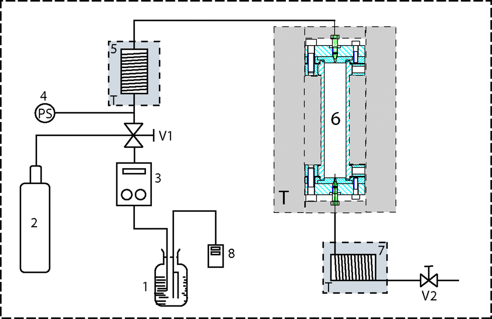 | ||
| Fig. 1 Schematic diagram of the apparatus for etching with SCW. 1-Water reservoir, 2-helium tank, 3-high pressure pump, 4-pressure sensor, 5-preheater coil, 6-reaction cell housing, 7-cooler, 8-oxymeter, V1-main control valve, V2-output control valve. Parts in the grey boxes labeled T were temperature controlled. | ||
Preparation of glass substrates
The commercial Cr and photoresist pre-coated substrates were exposed using a direct laser writer (μPG 101, Heidelberg Instruments, Heidelberg, Germany). The test pattern, defining the etched channels, was designed as a square net with 1 mm spacing and 10 μm line thickness. It was written across a 40 mm × 40 mm area of the substrate. The exposed area of the photoresist was removed by immersing the substrate in 2% aqueous tetramethylammonium hydroxide for 30 s. In the next step (hard baking) the substrate was placed on a hotplate (95 °C) for 30 min. Finally, the underlying Cr layer was removed by a chromium etchant (16.5 g of ammonium cerium(IV) nitrate and 4.2 ml of perchloric acid in 100 ml of distilled water). The preparation process was completed by cutting the substrate to 16 pieces of 10 mm × 10 mm chips using a dicing saw.Standard etching of glass substrates
The wet chemical etching process employing a buffered, HF-containing mixture was used as a reference method. The mixture was prepared from 40 g of ammonium fluoride dissolved in 55 ml of distilled water. The solution was heated on a hot plate to assist the dissolution of NH4F. Subsequently, the solution was transferred to a polypropylene container and 15 ml of 49% hydrofluoric acid was carefully added to the solution. The final glass etching solution contained 7.5 ml of the buffered HF, 82.5 ml of deionized water and 10 ml of 35% hydrochloric acid. The chip with a grid structure was inserted in a polypropylene beaker filled with 25 ml of glass etching solution and placed on a hot plate. The etching temperature was held at 50 °C or 75 °C for 40, 60 and 120 min.Etching of glass substrates with sub/supercritical water
The chip was inserted into the preheated extraction cell and quickly closed. The preheating step was included to minimize the time for thermal equilibration of the water-filled cell. Next, the cell was placed into the temperature-controlled jacket of the apparatus connected to the high-pressure system and flushed with nitrogen for 120 s to prevent oxidative processes. Filling of the cell with preheated water was carried out at the maximum flow rate of the pump (10 ml min−1). A two-stage process was used for pressurizing the cell. In the first step, the system was pressurized to a pressure slightly higher (+1 MPa) than the water vapor pressure at the adjusted temperature, followed by a 10 min equilibration time period for complete heating of the water and the sample. In the second step, the system was quickly pressurized to the required value and the countdown of the etching time was initiated. The final step of the process consisted of controlled depressurization and removal of water vapor by flushing the system with pressurized nitrogen.SEM and profilometry
Both the surface roughness and the quality of channel edge were evaluated by scanning electron microscopy (MIRA3, Tescan, a.s, Brno, Czech Republic) in InBeam mode at 300×, 1000× and 20![[thin space (1/6-em)]](https://www.rsc.org/images/entities/char_2009.gif) 000× magnification. The precise values of the channel width (w) and depth (d) together with the channel profile were measured with a 3D laser profilometer (model Contour GT X8, Bruker, Tucson, AZ, USA) and evaluated as 2D and 3D scans. A slight underetching of the chromium layer to a depth of 1–2 μm was observed under some experimental conditions. These minor flaws caused by the imperfections in the protective layer are typically eliminated during the bonding process and are less important in practical terms; however, such imperfections can cause variations during the channel width measurements in the surface plane. To obtain representative data and a correct correlation with the operating parameters the channel widths were always measured at half-depth (w0.5).
000× magnification. The precise values of the channel width (w) and depth (d) together with the channel profile were measured with a 3D laser profilometer (model Contour GT X8, Bruker, Tucson, AZ, USA) and evaluated as 2D and 3D scans. A slight underetching of the chromium layer to a depth of 1–2 μm was observed under some experimental conditions. These minor flaws caused by the imperfections in the protective layer are typically eliminated during the bonding process and are less important in practical terms; however, such imperfections can cause variations during the channel width measurements in the surface plane. To obtain representative data and a correct correlation with the operating parameters the channel widths were always measured at half-depth (w0.5).
Water density calculations
The density of water at a particular temperature and pressure was calculated from the Wagner–Pruss equation of state10 employing the software package developed by Wagner and Overhoff.11Results and discussion
The solvent properties of water (the density, the static relative permittivity, the cohesive energy density, and the ion product) can be tuned within very wide limits by adjusting the operating temperature and pressure. SCW is also well known for its ability to solubilize silicon dioxide, both in the crystalline form of quartz and in the form of amorphous silica.4,5In this work, the glass chips were etched in three regions: far below the water critical temperature (subcritical), directly at the critical temperature and above the water critical temperature (supercritical). The applied pressure varied from 13 MPa to 45 MPa and the etching time ranged from 5 min to 4 hours. The matrix of targeted tests included 43 experiments and the reference chips were etched with the HF-containing mixture.
Channel etching with subcritical water
Water below its critical point is still relatively incompressible; however, the temperature-induced changes in its properties are sufficient to exert a considerable impact on the etching process. The SEM pictures of channel crossings obtained by etching at 300 °C to 360 °C (Fig. 2a) for 30 min at 40 MPa show a gradual widening of channels as well as a progressing degree of underetching of the chromium layer with the rising temperature. Measurements of the channel profile by laser profilometry found four different channel geometry profiles for the density of water ranging from 0.764 to 0.649 g cm−3 (Fig. 2b). In microfluidic applications the typical width and depth of the channels are on the order of several tens to hundred micrometers. The best channel geometry to fit such requirements (43 μm, 61 μm) was achieved with the sample etched at 340 °C and 0.693 g cm−3. The etching power of subcritical water at this temperature and density is relatively low, requiring 30 min to etch a 40 μm deep channel. Moreover, the extended etching time results in excessive underetching of the protective Cr layer. A further increase in the etching temperature leads to a deeper channel but at the cost of a distorted channel profile (Fig. 2, chip no. 18).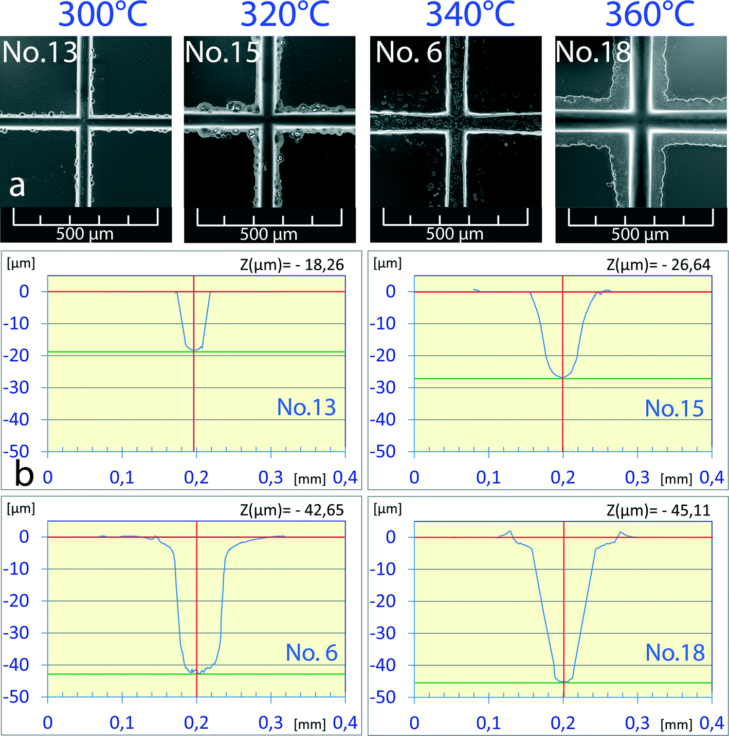 | ||
| Fig. 2 SEM pictures (a) and 2D profiles (b) of channel crossings etched at different temperatures. | ||
From the viewpoint of channel geometry, the best, clear channel profile was found at 300 °C (no. 13, 32 μm width), however, with a relatively shallow channel depth of 18 μm. In order to produce deeper channels the dependence of the channel depth on the etching time at a constant density of water was studied (Fig. 3). Etching time was set in the range of 15 to 240 min. Under these conditions no underetching defects were observed except for the longest time (no. 1, 4 h). The channel depth increased almost linearly with the etching time and the channel width simultaneously increased too. The etching rate was constant in both depth and width directions, and the w0.5/d ratio varied slightly from 1.8 to 2.0 for all samples in the series. For example, chip no. 1 (44 μm depth) reached a width of 79 μm, or chip no. 12 (26 μm depth) reached a width of 48 μm. The effect of increased etching time is more visible from 3D previews in Fig. 3: chips no. 1 (44 μm, 79 μm), no. 13 (18 μm, 32 μm) and no. 14 (13 μm, 26 μm).
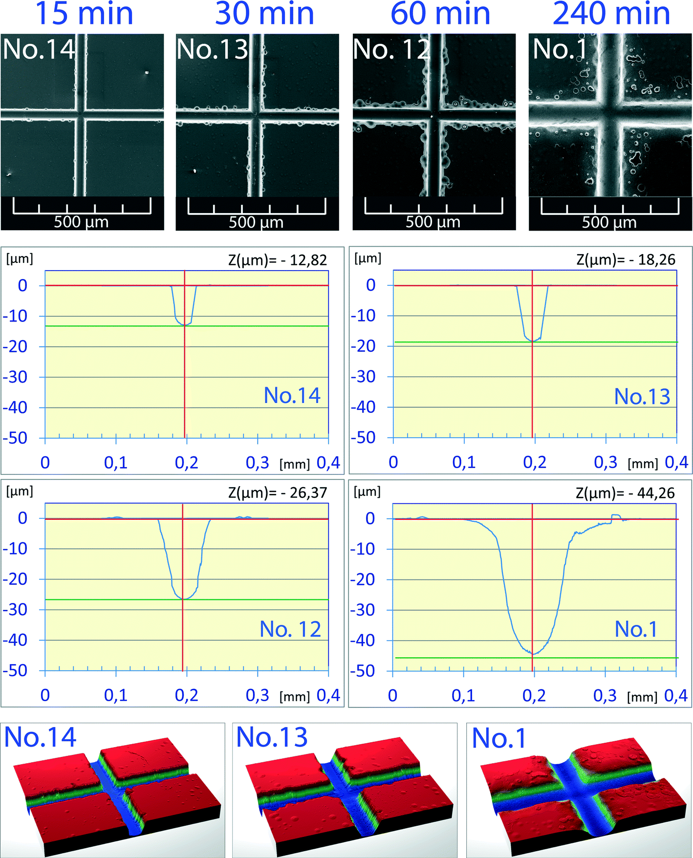 | ||
| Fig. 3 Dependence of channel depth on etching time at a constant density of 0.764 g cm−3 (40 MPa, 300 °C). | ||
Channel etching with supercritical water
The previous experiments indicate a positive effect of shorter etching time to minimize underetching of the chromium layer and testify to an increase in the etching power of water with the rising temperature. From this point of view, supercritical water should offer even better etching properties and very short etching times (minutes). The set of experiments with water above its critical temperature was carried out in the temperature range of 380 °C to 400 °C and at the pressure ranging from 10 MPa to 45 MPa in 5 MPa steps. Under these conditions the water density varied over a wide range from 0.038 g cm−3 to 0.614 g cm−3. The chips etched with supercritical water had a slightly lower w0.5/d ratio (1.4–1.6) compared to the chips etched with subcritical water (1.8–2.0). In addition, an interesting new phenomenon was observed during the experiments where part of the dissolved material was re-deposited above the original surface plane and produced rims along the channel edges (Fig. 4a, 6 μm high rims). While this effect may have a negative impact on the thermal bonding procedure, it might also bring new microfabrication possibilities. In this set of experiments it was found that this phenomenon appeared in all chips etched at the water density higher than 0.5 g cm−3. At lower water density, yet another phenomenon was observed, where practically all of the dissolved glass material has recrystallized, forming elevated edges, as shown in Fig. 4b–d. At present there is not enough information to support a conclusive explanation; however, the SEM images show that the hilly formations display a structure similar to that of monolithic silica.7 Therefore, these formations are probably composed of porous silicon dioxide rather than glass. The chips shown in Fig. 4a and b were etched with supercritical water at 400 °C and pressures of 45 MPa and 35 MPa, respectively. The difference in density was just 0.079 g cm−3 (0.554 g cm−3vs. 0.475 g cm−3) with a rather dramatic impact on the outcome. Fig. 4b, c and d show other examples of the chips etched below 0.500 g cm−3 with densities of 0.475 g cm−3, 0.215 g cm−3 and 0.064 g cm−3, respectively. On the basis of the above findings it can be assumed that future application of very high pressures (50–100 MPa) to increase the water density could suppress the “grow up” effect and offer new options for supercritical water microfabrication.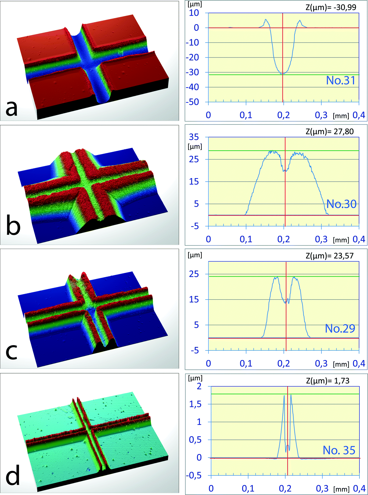 | ||
| Fig. 4 3D preview of chips etched above (a) and below (b, c, d) the 0.5 g cm−3 density of SCW. | ||
Channel etching with SCW at the critical temperature of water and comparison with HF-based etching
The experiments with subcritical water led to relatively shallow channels and long etching times, whereas the etching of chips with supercritical water was accompanied by the “grow up” effects. Thus, it appears that the borderline between those two conditions should be near the critical temperature of water. In an effort to optimize the channel parameters, notably the w0.5/d ratio, the experiments were carried out at 374 °C, just slightly above the critical temperature of water. To avoid the high-compressibility region near the critical point of water, the etching experiments were performed at supercritical pressures of 25 MPa, 35 MPa and 45 MPa with the corresponding densities of 0.513 g cm−3, 0.591 g cm−3 and 0.629 g cm−3, respectively. The etching time was fixed at 5 min. The chips etched under these conditions featured the best characteristics with narrow channels and the w0.5/d ratio was as low as 1.16 (Fig. 5a, SCW, 45 MPa). Furthermore, it has been observed that the w0.5/d ratio significantly decreased with the rising pressure, and it is very likely that the maximum operating pressure of the pump employed (50 MPa) was the only obstacle preventing achieving even lower w0.5/d values. The short etching time was not only practical but it also minimized the underetching or growing up of the silica layer at the channel edge. The surfaces of channels were homogenous and showed nearly the same structure for all densities (Fig. 5b, SCW).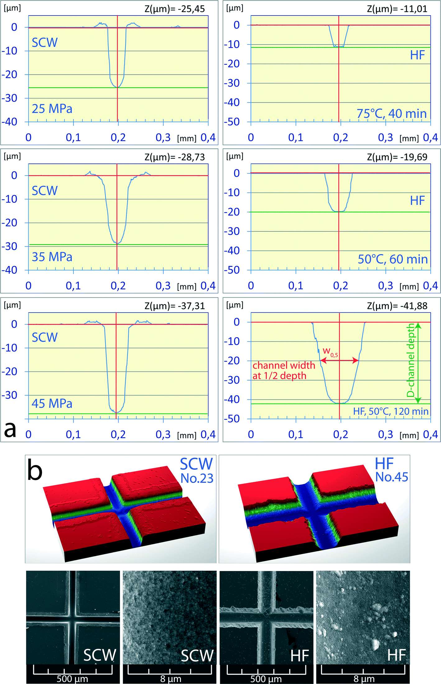 | ||
| Fig. 5 (a) Comparison of channel profiles etched with SCW at the critical temperature with those etched using the standard HF mixture. (b) 3D preview and SEM of channel surfaces etched with SCW and by the standard HF method. | ||
The quality of the results obtained with near-critical water is more evident in comparison with the chips etched by the standard procedure with the HF mixture (Fig. 5a, HF). The channels etched for 2 hours at 75 °C had a width of 83 μm and a w0.5/d of 2.0. Although the “grow up” effects do not occur in the standard method, the channel edges are rather irregular with distinct cavities caused by underetching of the Cr layer (Fig. 6, HF). On the other hand, the channels etched with near-critical water had sharp edges (D2) with steep walls and insignificant underetching zone up to 2 μm thick (D1), with the unremoved chromium layer and photoresist accounting for a substantial part of the zone thickness.
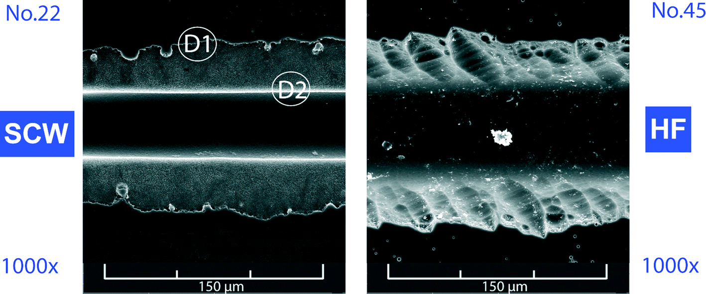 | ||
| Fig. 6 Comparison of the character of channel edges etched with the supercritical water (SCW) and hydrofluoric acid-based etchant. The channel depth (~40 μm) was the same in both cases. | ||
Experiments within this work were carried out in a wide range of temperatures and pressures influencing not only the water density but also the water solubility parameter, dielectric constant, and ion product. Apart from affecting the channel width and depth, the changes in the solvent properties also exert strong effects on the morphology of the channel surface. The surface structures were finer at moderate operating temperatures and pressures with short etching times. The surface roughness increased with rising temperature as well as with extended time of etching. The observed correlation between the operating conditions and the character of the channel surface structures can be very useful for preparation of special-purpose chips with specific requirements with regard to the channel surface roughness. One can easily imagine a two-step procedure of channel preparation where the chips with a desired w0.5/d ratio would be etched in the first step, and the channel surface would subsequently be modified under different operating conditions in the second step. Some examples of surface structures prepared in this study are shown in Fig. 7. The surface roughness (surface-to-volume ratio) can be fine-tuned for potential applications in separation and/or enzymatic microreactions;12 however, a detailed discussion is beyond the scope of this introductory article and will be presented separately.
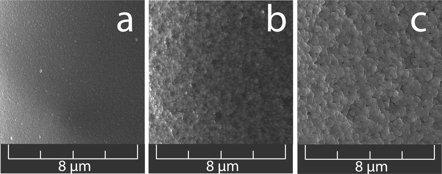 | ||
| Fig. 7 Different types of surface structures tunable by changing the SCW properties. (a) 300 °C, 40 MPa, 60 min; (b) 373 °C, 45 MPa, 5 min; (c) 400 °C, 45 MPa, 5 min. | ||
Conclusions
This work presents the potential of sub- and supercritical water to prepare glass microchip channels with the required parameters. The best results were achieved near the critical temperature of water where the channel depth could easily be controlled by pressure. In comparison to the standard HF-based etching procedure the etching time can be up to an order of magnitude faster. In addition, the resulting channels have superior quality, allowing a higher aspect ratio (w0.5/d = 1.16), smoother, or if required, more porous surface structure and well defined edges. The full exploitation of supercritical water as the etching agent appears to require operating pressures above 50 MPa. The subcritical water proved to be suitable for microfabrication of wider channels with a lower aspect ratio. The channel surface character can be independently modified with SCW in the second etching step. This particular feature represents an additional benefit of the water-based etching procedure that is impossible to achieve with the buffered, hydrogen fluoride mixtures.Acknowledgements
Financial support from the Grant Agency of the Czech Republic (P106/12/0522 and P206/12/G014), the European Social Fund (project no. CZ.1.07/2.3.00/20.0182 administered by the MEYS of the Czech Republic) and the institutional support RVO: 68081715 is acknowledged. Part of the work was realized in CEITEC – Central European Institute of Technology with research infrastructure supported by the project CZ.1.05/1.1.00/02.0068 financed by the European Regional Development Fund. We also wish to thank Michal Vasina for help with the experimental work.Notes and references
- M. J. Madou, Fundamentals of Microfabrication, CRC Press, 2nd edn, 2002, Fifth Printing, p. 723 Search PubMed.
- H. Weingärtner and E. U. Franck, Angew. Chem., Int. Ed., 2005, 44, 2672–2692 CrossRef PubMed.
- M. Azaroual and C. Fouillac, Appl. Geochem., 1997, 12, 55–73 CrossRef CAS.
- G. C. Kennedy, Econ. Geol., 1950, 45, 629–653 CrossRef CAS.
- R. O. Fournier and J. J. Rowe, Am. Mineral., 1977, 62, 1052–1056 CAS.
- A. Liebscher, Geofluids, 2010, 10, 3–19 CAS.
- P. Karásek, J. Planeta and M. Roth, Anal. Chem., 2013, 85, 327–333 CrossRef PubMed.
- K. Šlais, M. Horká, P. Karásek, J. Planeta and M. Roth, Anal. Chem., 2013, 85, 4296–4300 CrossRef PubMed.
- M. Horká, J. Šalplachta, P. Karásek, A. Kubesová, J. Horký, H. Matoušková, K. Šlais and M. Roth, Anal. Chem., 2013, 85, 6806–6812 CrossRef PubMed.
- W. Wagner and A. Pruss, J. Phys. Chem. Ref. Data, 2002, 31, 387–535 CrossRef CAS PubMed.
- W. Wagner and U. Overhoff, ThermoFluids. Interactive software for the calculation of thermodynamic properties for more than 60 pure substances, Springer, Berlin–Heidelberg, 2006 Search PubMed.
- J. Křenková, K. Klepárník and F. Foret, J. Chromatogr. A, 2007, 1159, 110–118 CrossRef PubMed.
Footnote |
| † Presented at The 6th International Symposium on Microchemistry and Microsystems, 30 July–1 August 2014, Singapore. |
| This journal is © The Royal Society of Chemistry 2015 |