
Molecular-ink route to 13.0% efficient low-bandgap CuIn(S,Se)2 and 14.7% efficient Cu(In,Ga)(S,Se)2 solar cells†
A. R.
Uhl
*,
J. K.
Katahara
and
H. W.
Hillhouse
*
Department of Chemical Engineering, Molecular Engineering and Sciences Institute, University of Washington, Box 351750, Seattle, WA 98195-1750, USA. E-mail: auhl@uw.edu; h2@uw.edu
First published on 7th December 2015
Abstract
A stable dimethyl sulfoxide (DMSO)-based ink containing a copper–thiourea–chloride complex and an indium–DMSO–chloride complex leads to 13.0% efficient CuIn(S,Se)2 (CIS) solar cells, which is a record for solution processed CIS. The formation of these complexes was found critical to control oxidation states and loss of metals during processing and to tailor the final composition of the absorber.
Broader contextSolar cells based on Cu(In,Ga)(S,Se)2 absorber layers have achieved the highest conversion efficiency amongst several thin film solar technologies but have so far struggled to translate their high performance into cost advantages on a module level. The use of printing processes has the potential to close that gap, provided high efficiency levels can be maintained and benign reagents for the material synthesis are employed. Additionally, low bandgap absorbers such as CuInSe2 are a highly attractive material for bottom cells in tandem devices, as their bandgap is an excellent match to some of the best performing hybrid perovskites. Here we present an ink composed of molecular complexes formed from metal chlorides, thiourea, and dimethyl sulfoxide and a fabrication route for low-bandgap CuIn(S,Se)2 absorbers whose device efficiency exceeds the performance of all previous non-vacuum methods and approaches device parameters of conventional cells formed by vacuum co-evaporation. The formation of complexes was found critical to control oxidation states and loss of metals during processing and tailor the composition of the absorber. These findings may pave the way for all-printed tandem solar modules and dramatically reduced cost of solar electricity. |
Photovoltaic devices are experiencing dramatic worldwide growth in installed capacity due to the increasingly favorable economics, the growing global energy demand, and rising concerns about climate change from greenhouse gas emissions.1 To date, polycrystalline Si solar cells are the market-leading technology, but thin film solar cells have caught up in performance.1,2 One of the most promising thin film technologies that has achieved conversion efficiencies up to 21.7% is based on Cu(In,Ga)(S,Se)2 absorber layers.3 The direct bandgap and high absorption coefficient enables complete light absorption within several microns only. By changing Ga/In and S/Se ratios, the bandgap can be tuned from 1.0 to 2.4 eV.4 However, device efficiency for the lowest bandgap (∼1.0 eV) still lags behind at 15.4%.5 These low bandgap variants are important for the development of tandem architectures with hybrid perovskite top cells since a 1.0 eV bandgap bottom cell is well current-matched with the bandgap of some of the best performing hybrid perovskites.6,7 Currently, the highest efficiency Cu(In,Ga)(S,Se)2 devices are made by vacuum evaporation, regardless of bandgap,2,3,5 but companies have struggled to translate the efficiencies from lab-scale cells to the module level.8 Non-vacuum solution-based printing techniques that exhibit inherent high material utilization, low capital expenditure (CAPEX), and high manufacturing throughput are an attractive alternative to vacuum deposition. However, cost advantages can only be realized if benign processing reagents are used and comparable efficiency values are achieved. Here, we report a solution processing route to CuIn(S,Se)2 (CIS) and Cu(In,Ga)(S,Se)2 (CIGS) that utilizes a benign molecular-ink that can be printed and is adaptable to roll-to-roll processing. The gallium-free CIS devices we report are a new World-record for solution processed photovoltaics with a bandgap of ∼1.0 eV (efficiency of 13.0%).
The direct deposition of molecular solutions – in contrast to nanoparticle dispersions – is particularly favorable, as it can use off-the-shelf chemicals, omits the need for nanoparticle synthesis and stabilization, and ensures intermixing of precursors on a molecular level. Several solution approaches have been developed, but challenges such as low device efficiency, carbon contamination, and the necessity to use toxic and explosive reagents could not be addressed simultaneously.9 The use of alcohol-based solvents and organic binder materials was seen to leave carbon-rich residual layers10,11 while other non-vacuum routes necessitate highly reactive gases (i.e. H2, H2S, or H2Se) to reduce precursor layers12–14 or toxic KCN etching to remove binary selenides.15 Notable efficiencies of 10.5% and 11.0% were presented by Hossain et al. and Berner et al. for Cu(In,Ga)(S,Se)2 and Cu(In,Ga)Se2 absorbers from a water spray-coating process and doctor-bladed metal carboxylates, respectively.16,17 McLeod et al. recently presented a sulfide nanoparticle based route with up to 15.0% efficient Cu(In,Ga)(S,Se)2 devices but further improvements could be hindered by carbonaceous impurities stemming from organic solvents or ligands.18 The highest efficiency from a pure solution process to date uses the carbon-free solvent hydrazine to achieve up to 15.2% efficient Cu(In,Ga)(S,Se)2 devices,19 but the toxic and explosive nature of the solvent may not be suitable for industrial implementation. Gallium-free absorbers from the same process have yielded up to 12.2% efficient devices with only slightly reduced bandgap from 1.16 to 1.15 eV, and 10.6% with a bandgap of 1.08 eV (12.7% and 10.6% using quantum efficiency data).20 However, low bandgap absorber materials such as CuInSe2 or low-sulfur CuIn(S,Se)2 are particularly important since they are excellent candidates for the bottom portion of tandem solar cells, e.g. in combination with a hybrid perovskite top cell.21
In this work, we present a novel solution deposition route that omits the use of highly toxic and explosive reagents by using inexpensive and commercially available metal chlorides, thiourea (TU), and dimethyl sulfoxide (DMSO) solvent. A clear precursor solution (Fig. 1a) is formed in which copper and indium ions are stabilized in the oxidation state +I and +III, which obviates the need for redox reactions before forming the I–III–VI2 absorber phase. Single crystal and powder X-ray diffraction (XRD) of precipitated crystals from the ink show crystalline Cu(TU)3Cl and In(DMSO)3Cl3 phases, which confirm both the oxidation state of cations and the important role of TU and DMSO as coordinating ligands (Fig. 1b–d). The ink is then applied on a substrate by spin-coating (or any other solution coating method) and enables conversion to CuIn(S,Se)2 or Cu(In,Ga)(S,Se)2 absorber layers by subsequent selenization with selenium vapor at temperatures below 550 °C. The resulting absorber layers exhibit high crystallinity and appear free of binary phases or carbon-rich layers. Combined thermogravimetric analysis (TGA) and Fourier transform infrared spectroscopy (FTIR) of the ink confirms the low evaporation or decomposition temperatures of the involved organic reagents (Fig. 1e). The early evaporation of DMSO around 100 °C is followed by the decomposition of TU between 180–230 °C, as seen by the accompanied release of CS2. Solar cells with CuIn(S,Se)2 absorber layers from this process exhibit conversion efficiencies up to 13.0% with bandgaps of only 1.0 eV, which represents the highest reported efficiency of a CuIn(S,Se)2 solar cell from any non-vacuum process, including the carbon-free hydrazine route. Early results with gallium-containing precursor inks resulted in up to 14.7% efficient solar cells, highlighting the potential of this route.
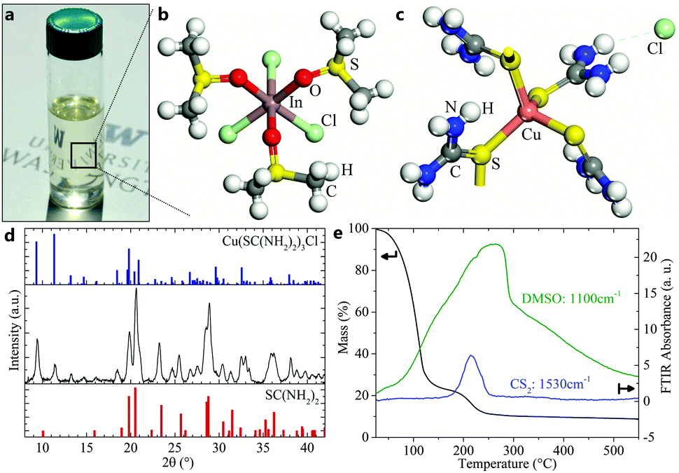 | ||
| Fig. 1 (a) Photograph of the final molecular ink. The photo shows a clear colorless solution, indicating the absence of solvated Cu(II) complexes. (b and c) Molecular structure of indium and copper complexes. The structure of In(DMSO)3Cl3 was determined by single-crystal XRD (see Table S3, ESI†) of crystals precipitated from an indium, TU, and DMSO ink. The Cu(TU)3Cl structure was identified from powder XRD (part d). (d) XRD pattern of a dried copper, TU, and DMSO ink that exhibits a mixture of TU and Cu(TU)3Cl crystals. (e) TGA with in situ FTIR analysis shows release of DMSO and CS2 during the decomposition of the ink. | ||
The mixture of DMSO and TU to prepare molecular inks was first developed in 2011 by Ki et al. for the application of Cu2ZnSn(S,Se)4 (CZTS) solar cells.22 In this method, Cu(CH3COO)2 and SnCl2 were shown to undergo a redox reaction that is aided by TU to produce a clear ink and leave metal cations in the desired oxidation state to react to CZTS.23 Thiourea is a well-known complexing agent that can release sulfur ions in alkaline media or upon thermal decomposition at 219 °C.24 Krzewska et al. have communicated its reducing capacity in connection with Cu(II) to form formamidine disulfide and various cuprous – but not cupric – complexes with thiourea.25 Reported complexes with Cu(I) in liquids range from 1–4 ligands, i.e. Cu(TU)1–4Cl, with the strongest coordination for the highest number of ligands.25 Cu+ is unstable in aqueous solutions and disproportionates to Cu0 and Cu2+.26 However, coordination with TU is able to stabilize the Cu(I) oxidation state in a soluble complex. Stable complexes for In(III) are reported as In(TU)3Cl3 with decomposition temperatures around 180 °C.27 DMSO is a non-toxic, dipolar, aprotic solvent that exhibits excellent solvation capabilities. Its hygroscopic and protophilic character effectively binds H2O molecules in the bulk solvent and precludes hydrolysis reactions.28 This facilitates its antioxidant properties and prevents precipitation of metal hydroxides as well as the premature decomposition of thiourea. DMSO was seen to form complexes with group III metals via bonding through oxygen, i.e. In(DMSO)3Cl3, In(DMSO)6Cl3, or Ga(DMSO)2Cl3.27,29 Thermal decomposition of In(DMSO)3Cl3 was found to start at 130 °C with a smooth decomposition curve.27 Copper complexes with DMSO are only known with its cupric form, i.e. Cu(DMSO)1–2Cl2.29
To confirm the coordination of metal cations in DMSO and DMSO/TU solutions, Raman spectroscopy was used to analyze the molecular vibrational modes. Fig. 2a shows the change in the DMSO C–S antisymmetric and thiourea C![[double bond, length as m-dash]](https://www.rsc.org/images/entities/char_e001.gif) S stretch with the addition of InCl3 and CuCl, respectively. The shift of the DMSO C–S antisymmetric stretch with InCl3 addition from 698 cm−1 to 720 cm−1 (and DMSO SO stretch from 1042 cm−1 to 1005 cm−1, Fig. S1, ESI†) is unaffected by the addition of thiourea.30 Furthermore, the CS stretch of thiourea (at 746 cm−1) is unaffected by InCl3 addition. In contrast, the CS stretching mode of thiourea is significantly lowered by the addition of CuCl to the ink.31 These results show that the oxygen in DMSO coordinates to the In(III) cation and that the sulfur in TU coordinates to the Cu(I) cation (corroborating findings in literature).
S stretch with the addition of InCl3 and CuCl, respectively. The shift of the DMSO C–S antisymmetric stretch with InCl3 addition from 698 cm−1 to 720 cm−1 (and DMSO SO stretch from 1042 cm−1 to 1005 cm−1, Fig. S1, ESI†) is unaffected by the addition of thiourea.30 Furthermore, the CS stretch of thiourea (at 746 cm−1) is unaffected by InCl3 addition. In contrast, the CS stretching mode of thiourea is significantly lowered by the addition of CuCl to the ink.31 These results show that the oxygen in DMSO coordinates to the In(III) cation and that the sulfur in TU coordinates to the Cu(I) cation (corroborating findings in literature).
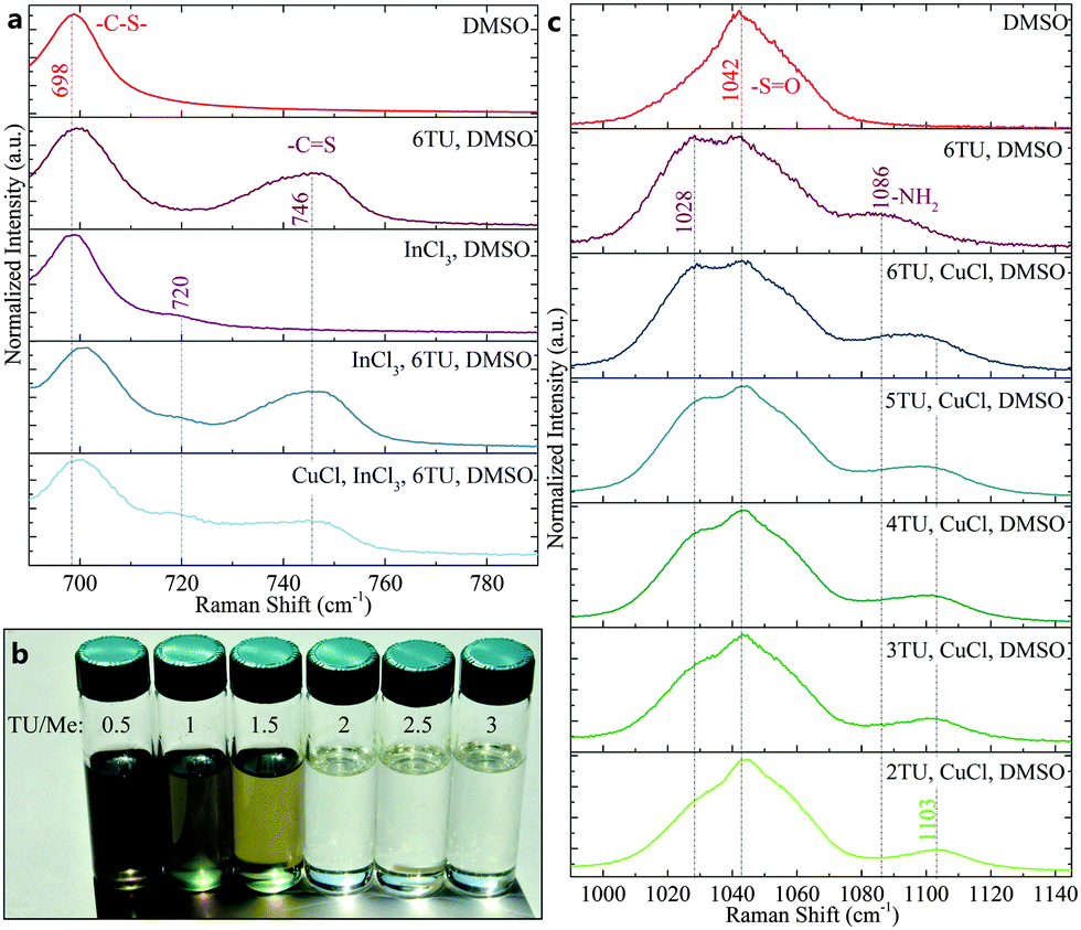 | ||
| Fig. 2 (a) Raman scattering spectra of liquid samples indicate coordination of In with DMSO and Cu with TU as well as the absence of In-TU interactions and Cu–DMSO interactions. (b) Inks with increasing thiourea to metal ratio from left to right. For a TU/Me ratio larger or equal to 2, inks are transparent and colorless, indicating a +I oxidation state of copper. (c) Shift of the SO stretch in DMSO to lower wavenumbers with TU addition suggests TU and DMSO coordination. The NH2 rocking mode of thiourea is affected by the addition of CuCl as seen by a shift to higher wavenumbers. The shift levels off at around TU/Cu ≤ 4. | ||
The importance of a strong coordination of Cu(I) to avoid its oxidation is exemplified in Fig. 2b where precursor inks with varying thiourea (TU) to metal (Me) ratio are depicted. Inks with TU/Me ratios of 0.5–1.5 exhibit greenish color, which could be related to CuCl2 or Cu(DMSO)2Cl2,29 and black crystallites that were identified as Cu(II)S (Fig. S2, ESI†). Inks with TU/Me ≥ 2 appeared colorless and visually transparent. A comparison of the thiourea NH2 rocking mode with different TU/Cu ratios can elucidate this behavior (Fig. 2c). The rocking mode of uncoordinated TU in DMSO appears at 1086 cm−1 while the mode of coordinated TU is shifted to 1103 cm−1. The observation of the coordinated NH2 mode from TU/Cu ratio of 2–4 suggests that up to 4 TU molecules can be coordinated by Cu(I) in solution.
Beyond that ratio, a shift towards the uncoordinated NH2 mode is detected. This is commensurate with literature that reported TU/Cu ≤ 3 for dried crystals but TU/Cu ≤ 4 in the ionic form.25 Moreover, both the DMSO SO stretch and the thiourea CS and NH2 modes in Fig. 2a and 2c exhibit either partial or complete shifts from literature values (CS: 731 cm−1, NH2: 1095 cm−1), which suggests the coordination of DMSO and TU.31 The TU/Me ratio in the ink was also found to have a strong effect on the final stoichiometry of the absorber (Table 1). By reducing the TU/Me ratio in the ink from 3 to 1, the indium loss throughout the process increased from 6% up to 59%. These now highly Cu-rich absorbers (Cu/In > 1) necessitate etching to remove conductive Cu–Se phases that would otherwise shunt the solar cell. Increased thiourea content in the ink also resulted in higher sulfur content in the films both after annealing and selenization. While all precursor layers appear chalcogen-poor (S/(Cu + In) < 1) after annealing despite the excess of TU, only the highest TU/Me ratio resulted in detectable sulfur content after selenization. Films were also prepared without filtering the inks prior to deposition, which led to lower indium loss (Table S1, ESI†). This suggests that some loss stems from the formation of small crystallites, particles, or coordination polymers that are formed with low TU concentration and filtered out of the ink prior to deposition.
| Cu/In | In loss (%) | S/(Cu + In) | Se/(S + Se) | ||
|---|---|---|---|---|---|
| TU/Me = 3 | Ink | 0.90 | 6 ± 2 | 18.35 | 0.00 |
| Precursor | 0.96 | 0.26 | 0.00 | ||
| Absorber | 0.95 | 0.01 | 0.99 | ||
| TU/Me = 2 | Ink | 0.91 | 18 ± 5 | 16.09 | 0.00 |
| Precursor | 1.11 | 0.24 | 0.00 | ||
| Absorber | 1.03 | 0.00 | 1.00 | ||
| TU/Me = 1 | Ink | 0.76 | 59 ± 4 | 14.11 | 0.00 |
| Precursor | 1.23 | 0.21 | 0.00 | ||
| Absorber | 1.17 | 0.00 | 1.00 | ||
Confirming ICP-MS findings, X-ray diffraction of the precursor and absorber layers shows the chalcopyrite phase for both layers, with the addition of MoSe2 for the selenized case (Fig. 3a). The peak narrowing and shift towards lower diffraction angles from precursor to absorber is indicative of grain growth and the substitution of sulfur by selenium. The inset depicts the peak shift of the (112) orientation in the absorber layers with varying TU/Me ratios. As expected from the ICP-MS data in Table 1, only TU/Me = 3 results in a detectable presence of sulfur in the absorber. Absorber layers from the described process appear free of residual carbon-rich layers and with large grains around 0.5 μm (Fig. 3b). Apart from some small void inclusions, the CuIn(S,Se)2 absorbers exhibit a dense microstructure and thickness around 1 μm. Fig. 3c visually summarizes the deposition process in three consecutive steps: (i) the application of the molecular precursor ink onto the Mo-coated glass substrate. Metal cations are stabilized by TU and DMSO ligands in oxidation state +I and +III; (ii) annealing of the film to decompose organic ligands and form nanocrystalline domains of CuInS2; and (iii) second annealing under Se vapor to facilitate the ion exchange from sulfur to selenium and concurrent grain growth.
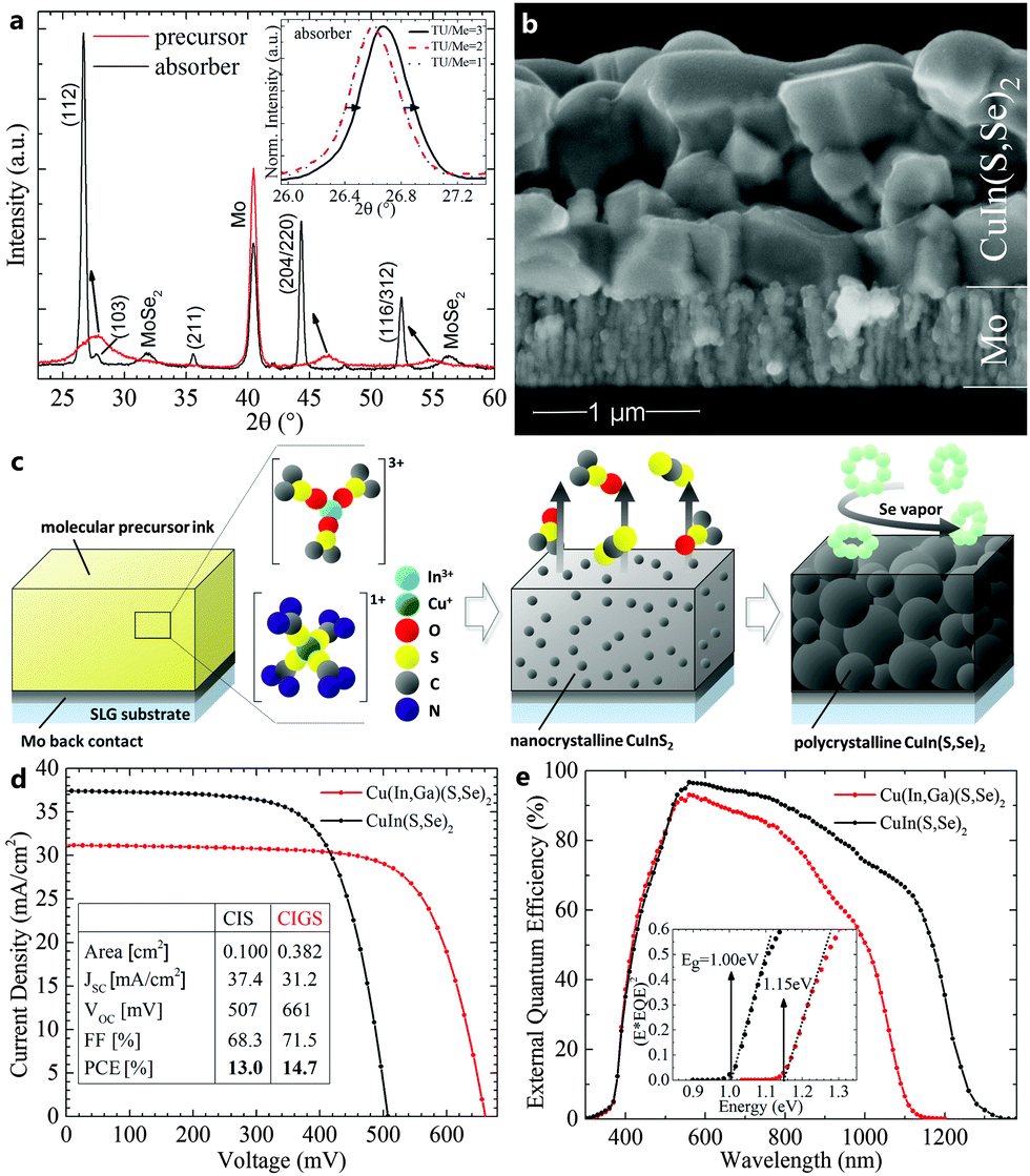 | ||
| Fig. 3 (a) XRD patterns of precursor and selenized films show crystalline phase of CuInS2 and CuIn(S,Se)2, respectively. Narrowing peaks and shift to lower diffraction angles can be attributed to crystal growth and substitution of sulfur with selenium. Inset confirms the higher sulfur content of absorbers from inks with TU/Me = 3. (b) SEM cross section of an absorber layer as obtained after ink depostition and selenization. (c) Schematic drawing of the process flow from deposited molecular ink to dried precursor film, to polycrystalline absorber. The tailored metal coordination by organic complexes stabilizes oxidation states of cations, reduces metal loss, and allows for clean decomposition upon heat treatment. (d) Active area efficiencies of up to 13.0% were obtained, which exhibits the highest value for a device with a non-vacuum obtained CuIn(S,Se)2 absorber. (e) External quantum efficiency measurements confirm minimum bandgaps of absorbers and high current collection of the devices. | ||
Solar cells were completed by the deposition of CdS/ZnO/ITO window layers, Ni/Al contacts, and a MgF2 antireflection coating. Devices with CuIn(S,Se)2 absorber layers exhibit up to 13.0% active-area power conversion efficiency under standard testing conditions with simulated AM1.5 illumination (with 37.4 mA cm−2, 68.3% FF, 507 mV), which, to the best of our knowledge, is the highest reported efficiency for any non-vacuum deposited CuIn(S,Se)2 solar cell to date.14,20,32 Early results with gallium-containing inks resulted in up to 14.7% active-area power conversion efficiency devices with increased open-circuit voltage (Voc) and fill factor (FF) (31.2 mA cm−2, 71.5% FF, 661 mV) (Fig. 3d). The corresponding external quantum efficiency (EQE) measurements (Fig. 3e) confirm bandgaps of 1.00 eV and 1.15 eV, while the calculated current densities (Jsc) from EQE of 37.9 and 31.1 mA cm−2 agree well with the data from current-voltage measurements for the CISSe2 and CIGSSe2 devices, respectively.
The quality of the solution-processed absorber layers becomes particularly apparent in comparison with devices using vacuum obtained absorber layers of similar bandgaps. Highest efficiency CuInSe2 solar cells (Egap = 0.97 eV) were obtained by both Uppsala University and NREL with efficiencies up to 15.4% (active area, 41.2 mA cm−2, 72.6% FF, 515 mV) and 14.5% (total area, 41.1 mA cm−2, 71.9% FF, 491 mV), respectively.5,33 While Jsc and FF are still lower for our CIS device, which points towards absorption, collection, or resistive losses, it is noteworthy that our Voc values are comparable to or exceed the vacuum fabricated record CIS devices above. This suggests that absorbers from our non-vacuum processes may be able reach efficiencies comparable to those from state-of-the-art vacuum processes while requiring only a fraction of the processing costs.
Conclusions
We have presented a novel molecular-ink route to deposit Cu(In,Ga)(S,Se)2 type absorber layers. The process employs readily available metal chlorides, thiourea, and DMSO to form stable inks that can be deposited via non-vacuum printing methods. Thiourea and DMSO were shown to coordinate copper and indium in oxidation state +I and +III, respectively. High TU/Me ratios are essential to avoid the oxidation of Cu(I), prevent the loss of indium, and tailor the S/Se ratio in the final absorber. Intermediate sulfide precursor layers can be converted with simple Se vapors, which omits the need for highly toxic or explosive conversion gases. The resulting stoichiometrically controlled absorbers appear free from carbon-rich layers and phase impurities and render additional etching steps unnecessary. Photovoltaic devices of up to 13.0% and 14.7% were obtained for CuIn(S,Se)2 and Cu(In,Ga)(S,Se)2 absorbers with a bandgap of 1.00 and 1.15 eV, respectively. This represents the highest reported efficiency for a solar cell with non-vacuum obtained CuIn(S,Se)2 absorber and is the first time that cells from a non-vacuum approach could reach Vocs of vacuum-obtained absorbers. This challenges traditional conceptions of inherently inferior material properties for non-vacuum obtained semiconductor layers and the use of organic reagents for solution processing in general.Acknowledgements
ARU acknowledges the Swiss National Science Foundation (SNSF) under project number P2EZP2_152168 for salary support. HWH and JKK acknowledge salary support from the DOE SunShot NextGen2 program (DE-EE0005321) and the UW Clean Energy Institute. HWH also acknowledges the University of Washington Rehnberg endowment for financial support for supplies and expenses and benefits for ARU. The NanoTech (NTUF) user facility is acknowledged for powder XRD and SEM measurements. The authors thank Warren Pinkard, Richard Caulkins, Prof. Werner Kaminsky, Sean Yeung, and Tuesday Kuykendall for help with molecular models, solution preparation, XRD, ICP-MS, and TGA/FTIR measurements, respectively.References
- B. K. Sahu, Renewable Sustainable Energy Rev., 2015, 43, 621–634 CrossRef.
- A. Chirilă, P. Reinhard, F. Pianezzi, P. Bloesch, A. R. Uhl, C. Fella, L. Kranz, D. Keller, C. Gretener, H. Hagendorfer, D. Jaeger, R. Erni, S. Nishiwaki, S. Buecheler and A. N. Tiwari, Nat. Mater., 2013, 12, 1107–1111 CrossRef PubMed.
- P. Jackson, D. Hariskos, R. Wuerz, O. Kiowski, A. Bauer, T. M. Friedlmeier and M. Powalla, Phys. Status Solidi RRL, 2015, 9, 28–31 CrossRef CAS.
- M. Bär, W. Bohne, J. Röhrich, E. Strub, S. Lindner, M. C. Lux-Steiner, C.-H. Fischer, T. P. Niesen and F. Karg, J. Appl. Phys., 2004, 96, 3857 CrossRef.
- J. Hedstrom, H. Ohlsen, M. Bodegard, A. Kylner, L. Stolt, D. Hariskos, M. Ruckh and H. Schock, 23rd IEEE Phot. Spec. Conf. (PVSC), 1993, 364–371 Search PubMed.
- H. Zhou, Q. Chen, G. Li, S. Luo, T.-B. Song, H.-S. Duan, Z. Hong, J. You, Y. Liu and Y. Yang, Science, 2014, 345, 542–546 CrossRef CAS PubMed.
- F. Meillaud, A. Shah, C. Droz, E. Vallat-Sauvain and C. Miazza, Sol. Energy Mater. Sol. Cells, 2006, 90, 2952–2959 CrossRef CAS.
- M. A. Green, K. Emery, Y. Hishikawa, W. Warta and E. D. Dunlop, Prog. Photovoltaics, 2015, 23, 1–9 Search PubMed.
- H. Azimi, Y. Hou and C. J. Brabec, Energy Environ. Sci., 2014, 7, 1829–1849 CAS.
- M. Kaelin, D. Rudmann, F. Kurdesau, H. Zogg, T. Meyer and A. N. Tiwari, Thin Solid Films, 2005, 480–481, 486–490 CrossRef CAS.
- A. R. Uhl, C. Fella, A. Chirilă, M. R. Kaelin, L. Karvonen, A. Weidenkaff, C. N. Borca, D. Grolimund, Y. E. Romanyuk and A. N. Tiwari, Prog. Photovoltaics, 2012, 20, 526–533 CAS.
- S. J. Park, J. W. Cho, J. K. Lee, K. Shin, J. H. Kim and B. K. Min, Prog. Photovoltaics, 2015, 22, 122–128 Search PubMed.
- A. Duchatelet, T. Sidali, N. Loones, G. Savidand, E. Chassaing and D. Lincot, Sol. Energy Mater. Sol. Cells, 2013, 119, 241–245 CrossRef CAS.
- B. M. Basol, Thin Solid Films, 2000, 361–362, 514–519 CrossRef CAS.
- A. R. Uhl, P. Fuchs, A. Rieger, F. Pianezzi, C. M. Sutter-Fella, L. Kranz, D. Keller, H. Hagendorfer, Y. E. Romanyuk, F. LaMattina, S. Yoon, L. Karvonen, T. Magorian-Friedlmeier, E. Ahlswede, D. VanGenechten, F. Stassin and A. N. Tiwari, Prog. Photovoltaics, 2015, 23, 1110–1119 CAS.
- M. A. Hossain, Z. Tianliang, L. K. Keat, L. Xianglin, R. R. Prabhakar, S. K. Batabyal, S. G. Mhaisalkar and L. H. Wong, J. Mater. Chem. A, 2014, 3, 4147 Search PubMed.
- U. Berner and M. Widenmeyer, Prog. Photovoltaics, 2015, 23, 1260–1266 CAS.
- S. M. McLeod, C. J. Hages, N. J. Carter and R. Agrawal, Prog. Photovoltaics, 2015, 23, 1550–1556 CAS.
- T. K. Todorov, O. Gunawan, T. Gokmen and D. B. Mitzi, Prog. Photovoltaics, 2015, 21, 82–87 Search PubMed.
- W. Liu, D. B. Mitzi, M. Yuan, A. J. Kellock, S. J. Chey and O. Gunawan, Chem. Mater., 2009, 22(3), 1010–1014 CrossRef.
- C. D. Bailie, M. G. Christoforo, J. P. Mailoa, A. R. Bowring, E. L. Unger, W. H. Nguyen, J. Burschka, N. Pellet, J. Z. Lee, M. Grätzel, R. Noufi, T. Buonassisi, A. Salleo and M. D. McGehee, Energy Environ. Sci., 2014, 8, 956–963 Search PubMed.
- W. Ki and H. W. Hillhouse, Adv. Energy Mater., 2011, 1, 732–735 CrossRef CAS.
- H. Xin, J. K. Katahara, I. L. Braly and H. W. Hillhouse, Adv. Energy Mater., 2014, 4, 1301823 Search PubMed.
- S. Wang, Q. Gao and J. Wang, J. Phys. Chem. B, 2005, 109, 17281–17289 CrossRef CAS PubMed.
- S. Krzewska, H. Podsiadły and L. Pajdowski, J. Inorg. Nucl. Chem., 1980, 42, 89–94 CrossRef CAS.
- I. V. Mironov and L. D. Tsvelodub, J. Solution Chem., 2015, 25, 315–325 CrossRef.
- A. J. Carty and D. G. Tuck, J. Chem. Soc. A, 1966, 1081–1087 RSC.
- E. Buncel, R. A. Stairs and H. Wilson, The Role Of The Solvent In Chemical Reactions, Oxford University Press, Oxford, 2003, pp. 104–115 Search PubMed.
- W. L. Reynolds, in Progress In Inorganic Chemistry, ed. S. J. Lippard, John Wiley & Sons, Inc., New York, 1970, vol. 12, pp. 1–99 Search PubMed.
- W. N. Martens, R. L. Frost, J. Kristof and J. Theo Kloprogge, J. Raman Spectrosc., 2002, 33, 84–91 CrossRef CAS.
- T. Ishiguro, E.-I. Suzuki, A. Y. Hirakawa and M. Tsuboi, J. Mol. Spectrosc., 1980, 83, 360–372 CrossRef CAS.
- J. F. Guillemoles, J. P. Connolly, O. Ramdani, O. Roussel, D. Guimard, V. Bermudez, N. Naghavi, P. P. Grand, L. Parissi, J. Kurdi, J. Kessler, O. Kerrec and D. Lincot, J. Nano Res., 2008, 4, 79–89 CrossRef CAS.
- J. A. M. AbuShama, S. Johnston, T. Moriarty, G. Teeter, K. Ramanathan and R. Noufi, Prog. Photovoltaics, 2004, 12, 39–45 CAS.
Footnote |
| † Electronic supplementary information (ESI) available: Experimental details, additional XRD, Raman, ICP-MS, and device characterization. CCDC 1423406. For ESI and crystallographic data in CIF or other electronic format see DOI: 10.1039/c5ee02870a |
| This journal is © The Royal Society of Chemistry 2016 |