
 Open Access Article
 This Open Access Article is licensed under a
 Creative Commons Attribution 3.0 Unported Licence
Depth probing of the hydride formation process in thin Pd films by combined electrochemistry and fiber optics-based in situ UV/vis spectroscopy†
Björn
Wickman
*,
Mattias
Fredriksson
,
Ligang
Feng
 ,
Niklas
Lindahl
,
Johan
Hagberg
and
Christoph
Langhammer
*
,
Niklas
Lindahl
,
Johan
Hagberg
and
Christoph
Langhammer
*
Department of Applied Physics, Chalmers University of Technology, SE-412 96 Göteborg, Sweden. E-mail: bjorn.wickman@chalmers.se; clangham@chalmers.se
First published on 25th June 2015
Abstract
We demonstrate a flexible combined electrochemistry and fiber optics-based in situ UV/vis spectroscopy setup to gain insight into the depth evolution of electrochemical hydride and oxide formation in Pd films with thicknesses of 20 and 100 nm. The thicknesses of our model systems are chosen such that the films are thinner or significantly thicker than the optical skin depth of Pd to create two distinctly different situations. Low power white light is irradiated on the sample and analyzed in three different configurations; transmittance through, and, reflectance from the front and the back side of the film. The obtained optical sensitivities correspond to fractions of a monolayer of adsorbed or absorbed hydrogen (H) and oxygen (O) on Pd. Moreover, a combined simultaneous readout obtained from the different optical measurement configurations provides mechanistic insights into the depth-evolution of the studied hydrogenation and oxidation processes.
1. Introduction
Analytical electrochemistry is very sensitive in the meaning that currents corresponding to fractions of a monolayer of species on the sample surface are easily measured. However, it is important to note that the measured current only reflects the net electrochemical reactions and that it is neither possible to obtain direct information about which reactions that are taking place, nor to derive the state of the electrode. Therefore, combining electrochemistry with an additional characterization or analysis tool is an often necessary and very useful way to obtain more and complementary information about processes occurring on or inside the electrode, and about its state. For this purpose, numerous techniques complementing electrochemistry have been demonstrated, including mass spectrometry (MS),1–3 quartz crystal microbalance (QCM),4–7 optical techniques like vibrational spectroscopy,8 infrared transmittance and reflectance spectroscopy,9 ellipsometry,10 optical microscopy,11,12 and synchrotron based X-ray spectroscopy.13 All these methods have in common that they rely on relatively advanced experimental setups and – where applicable – complex optics in order to obtain signals with a satisfying signal-to-noise ratio and resolution.More specifically for the topic of metal hydride formation that is in focus here, it has also been shown that direct optical reflectance and transmission measurements combined with electrochemistry are very useful, for example in the context of so-called switchable mirrors.14,15 Conceptually, these studies are reminiscent of the “hydrogenography” approach developed for hydrogenation from the gas phase.16,17
Here we further develop this general concept by combining electrochemistry with in situ UV/vis spectroscopy in the transmittance and front- and back-side specular reflectance mode. In particular, we show that by a simultaneous readout from two of the different modes, mechanistic insights into the depth-evolution of the surface oxidation, as well as the hydride formation process in thin Pd films can be obtained. Moreover, to simplify the required hardware, we demonstrate that this becomes possible by solely relying on off-the-shelf, flexible and robust fiber optics.
1.1 Electrochemical hydride formation in palladium
It is well known that Pd can form a hydride under electrochemical conditions18–22 and that the H/Pd atomic ratio can be as high as 0.62–0.67, which is similar to what is typically obtained in the gas phase.23–25 To reduce problems of high currents, which cause iR-drop and bubble formation at the counter electrode, and diffusion limitations that increase the timescale of experiments, the Pd film must be relatively thin. These thin Pd electrodes are sometimes referred to as limited volume electrodes (LVE)26,27 and typically mean that the Pd film is between a few monolayers (ML) up to a few μm thick.In the electrochemical system it is possible to form PdHx from either H2 gas dissolved in the electrolyte or via protons from solution.19 In the present study we have only considered the latter pathway. The electrochemical hydride formation in an acidic environment, where protons react with Pd, takes place according to:
| Pd + xH+ + xe− → PdHx | (1) |
2. Experimental
2.1 Electrode fabrication
Borofloat® glass (Schott Scandinavia AB) was cut into 15 × 15 × 1 mm pieces and cleaned ultrasonically in consecutive baths of acetone, isopropanol, and Milli-Q water. Pd films of 20 or 100 nm thickness were deposited using electron beam evaporation in a vacuum (Lesker PVD 225 with a base pressure of <5 × 10⁻⁷ mbar). Prior to deposition of Pd, a 3 nm Ti adhesion layer was deposited in the same equipment.2.2 Combined electrochemical and fiber optic in situ UV/vis measurements
Prior to the measurements, the Pd film samples were cleaned using the same ultrasonic procedure as described for the substrates above. A piece of copper tape was attached to the sample before mounting in the setup for combined electrochemistry and optical UV/vis measurements shown in Fig. 1. Subsequently the copper tape was connected as a working electrode (WE). The in-house constructed measurement cell is composed of three sections, all made of PEEK (polyetheretherketone). The sample is clamped between the lower and middle section of the cell and sealed with a Viton O-ring. The active electrode area exposed inside the O-ring is 0.95 cm2. Between the middle and upper sections, a quartz window is clamped and sealed with another Viton O-ring. The volume created in the middle section, between the sample and the quartz window, is about 0.475 cm3. An electrolyte inlet and outlet enable filling of the cell and allow it to be operated under continuous flow conditions. A Pt wire as a counter electrode (CE) was inserted into the middle section. A halogen light source (Avantes AvaLight-Hal) was used from which an optical fiber (Ocean Optics vis-NIR 600 μm core) guided the light to the cell and illuminated the sample at normal incidence. For transmittance measurements, the light transmitted through the electrode to the opposite side of the cell was collected with a collimating lens and a second optical fiber (Ocean Optics vis-NIR 600 μm core). For reflectance measurements a reflectance probe (Avantes FCR-7xx400-2-BX) was used to both illuminate and collect specularly reflected light (at normal incidence). To allow collection of two optical signals simultaneously, a beam combiner (Avantes BSA-DA) was utilized. A fiber coupled fixed grating spectrometer (Avantes AvaSpec-HS1024x58TEC) was used to analyze the transmitted or reflected light. In our system, optical spectra can be obtained at a maximal sampling frequency of 200 Hz and cover the wavelength range between 300 and 1100 nm, with each pixel of the CDD corresponding to 1 nm. In this study we use the averaged value of 20–50 spectra acquired with an integration time of 2–5 ms corresponding to a sampling rate of 5–10 Hz. In the analysis, we used the 700 ± 5 nm spectral range for the readout as this yielded the best signal to noise ratio (S/N) due to the favorable combination of lamp emission intensity and the efficiency of the spectrometer grating. Representative values of S/N, comparing the signal from a Pd surface in the metallic state (i.e. no adsorbates, collected in the double layer region) with the fully hydride state and the surface oxide state are 60![[thin space (1/6-em)]](https://www.rsc.org/images/entities/char_2009.gif) 500 and 450, respectively. Fig. S1 in the ESI,† shows results for a series of different wavelengths where it can be seen that the best signal to noise ratio is found at around 700–800 nm. We note that this optimum condition can easily be adjusted to other wavelengths by the alternative choice of light source, spectrometer, or grating, if desired.
500 and 450, respectively. Fig. S1 in the ESI,† shows results for a series of different wavelengths where it can be seen that the best signal to noise ratio is found at around 700–800 nm. We note that this optimum condition can easily be adjusted to other wavelengths by the alternative choice of light source, spectrometer, or grating, if desired.
 | ||
| Fig. 1 Schematic illustration of the measurement setup used to perform the combined electrochemical and in situ UV/vis optical measurements (a), and of how the light was irradiated and collected with respect to the sample (b). | ||
To define the optical readout and set a zero-baseline value, we applied a self-referencing strategy. In other words, we defined the transmittance or reflectance spectrum obtained at a potential of 0.4 V, which is roughly in the middle of the double layer region where no species are adsorbed on Pd (i.e. a clean metallic surface), as the baseline level of our experiment and divided the continuously measured spectra during the experiment with the initially taken baseline at 0.4 V. The signal from a transmittance measurement, which we here present as a change in optical extinction, ΔExt, is defined as:
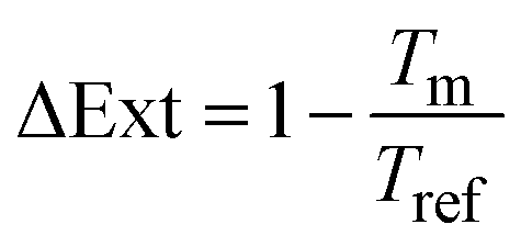 | (2) |
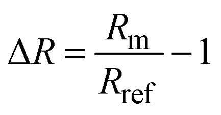 | (3) |
The electrolyte used was 0.5 M H2SO4 prepared from Millipore Milli-Q water and Reagent Grade concentrated H2SO4 (Sigma Aldrich). During the measurements, the electrolyte was continuously bubbled with N2 to remove dissolved O2. Tygon tubing was used to transport the electrolyte from a reservoir to the cell inlet and from the cell outlet to a glass beaker where an Hg/Hg2SO4 reference electrode (RE) (XR200, Radiometer) was placed. The electrochemical measurements were conducted in regular three-electrode configuration using a Gamry instruments Reference 600 potentiostat. All potentials reported herein have been converted to the reversible hydrogen electrode (RHE) scale. To synchronize the timescales of the electrochemical and the UV/vis spectroscopy measurements, a digital trigger was sent from an in-house developed Matlab program that controls the UV/vis experiment and picked up by the potentiostat. The synchronization was measured to be accurate within ±10 ms. The uncompensated resistance, Ru, was measured with the routine “Get Ru” in the Gamry Framework software for each sample and all subsequent electrochemical measurements were done with positive feedback iR-compensation at 85% of the measured Ru. The remaining 15% were not corrected for after the measurements. Thus the data shown here are iR-compensated to 85%. It can be mentioned that all samples with 20 nm Pd had an Ru between 10–12 Ω, and with the rather slow scan rate of 5 mV s−1, the currents were quite moderate (<1.8 mA). Thus the iR-compensation does not greatly affect the results (at 1.8 mA the remaining potential drop is less than 3 mV).
2.3 Pd film microstructure characterization
The morphology of the evaporated Pd films was characterized by scanning electron microscopy (SEM, Zeiss Supra 60) operating at 10 kV in the secondary electron mode. Fig. 2 shows 20 and 100 nm Pd films as deposited and after the films had been cycled until the CV and hydride charge were stable (between 15–20 cycles). Thus, the images to the right in Fig. 2 display the state of the films during measurements. As can be seen, the as deposited films are rather smooth with a grain size on the order of 10 nm. After a number of hydrogenation/dehydrogenation cycles there are clear changes in the film structure. For the 20 nm film larger domains appear but the film seems to stay rather smooth. For the 100 nm film the changes are more pronounced and large crystallite domains (on the order 100 nm) are present, and the film appears to be rougher. We note here that despite these microstructural differences between the 20 nm and 100 nm films, qualitative comparison of their surface oxidation and hydrogen sorption behavior should be uncomplicated. | ||
| Fig. 2 Scanning electron microscopy images of 20 and 100 nm Pd films, as fabricated (a and b) and after electrochemical conditioning (c and d). The magnification is identical in all figures. | ||
3. Results and discussion
3.1 Cyclic voltammetry and optical response
Fig. 3 shows the results of cyclic voltammetry at 5 mV s−1 between −0.0677 to 1.4 V together with corresponding optical response for a 20 and a 100 nm Pd film. | ||
| Fig. 3 Cyclic voltammetry and corresponding UV/vis optical extinction and reflectance signals for 20 and 100 nm Pd film. (a) current (b) reflectance change from top, (c) reflectance change from bottom, and (d) extinction measured in 0.5 M H2SO4 with a scan rate of 5 mV s−1. The optical data are an average of the wavelengths at 700 ± 5 nm. The insets show the Pd oxide region magnified for clarity. | ||
When the potential is reversed and scanned anodically, there is a first small, broad peak close to 0 V which is attributed mainly to the oxidation of H2 produced at the lower potentials, and which has not diffused away from the electrode surface.24 The main peak corresponds to the oxidation of PdHx and shows a maximum at about 0.05 V. Soon after, the depletion of the β-phase is complete. It appears as the decomposition of the α-phase and desorption of adsorbed H on the Pd surface is more or less reversible and follows the same path as during the absorption and hydride formation.
At about 0.8 V in the anodic scan direction, OH adsorption on Pd sets in and at higher potentials the oxidation of the Pd surface begins. When the scan is reversed, the oxide covered surface is stable down to about 0.75 V, where reduction of Pd oxide sets in. Below 0.6 V, the Pd surface is again metallic, with no adsorbed species.
It can also be seen in Fig. 3b–d that there is a hysteresis between the hydride formation and decomposition, which is wider for the 100 nm film compared to the 20 nm one. In general terms this indicates the presence of a barrier involved in either or both the hydride formation and decomposition reactions. For hydrogenation from the gas phase, the hysteresis is attributed to lattice strain induced by the presence of hydrogen in the metal. This strain creates an energy barrier that needs to be surmounted in order for the hydride to form or decompose.36–38
Another important feature that can be observed is that the optical signals level off and saturate at the lowest potentials. In addition, just before −0.0677 V where the potential is reversed, there is no hysteresis. This is in good agreement with the picture of the phase transition to the β-phase PdHx being completed at these potentials, and that a larger part of the current now goes into H2 evolution, which should not affect the optical measurements, unless H2 bubbles are formed.
In the oxidation regime of the CV (>0.7 V) the reflectance and extinction signals drop almost linearly as the oxide layer is formed on the surface. When the scan is reversed, the signal stays constant until the reduction of Pd oxide starts at about 0.75 V and the signal increases to almost the same level as before oxidation. The fact that the signal is not completely reversible is most likely a result of Pd corrosion, which occurs when cycling to these high potentials,39 and/or additional restructuring of the Pd surface, as seen in Fig. 2. However, the amount of Pd lost in each cycle is still quite low,20,39 and the number of full cycles after the conditioning on each sample was kept at a minimum (<20 cycles per sample). Thus, the amount of Pd can be considered to be constant during the measurements.
Comparing the reflectance signal measured from the front for the 20 and 100 nm Pd films (Fig. 3b) it can be seen that they are qualitatively very similar, except for a few smaller deviations: (i) the signal amplitude (difference between metallic Pd and hydride or oxide) is larger for the 20 nm film, (ii) there is a larger hysteresis between the hydride formation/decomposition for the 100 nm film, and (iii) the hydride phase seems to reach a more saturated stage in the 100 nm film. The reflectance traces measured from the back side of the two samples (Fig. 3c) are qualitatively similar; however, with the important difference that there is no signal for the oxide formation on the 100 nm film because the film is thicker than the optical skin depth of Pd (which is ca. 50 nm). This nicely illustrates the surface sensitivity of our approach and the possibility of discriminating between surface and bulk processes in the electrode material.
3.2 Hydride formation/decomposition analysis
To gain deeper insight into the three-dimensional evolution of the hydride formation in Pd films, and to illustrate the type of information that can be obtained using the approach presented here, normalized reflectance changes measured from the front and back sides of the 20 nm (two separate experiments) and 100 nm (measured simultaneously) Pd films are shown in Fig. 4a and 5a, respectively. Subfigures b and c, in Fig. 4 and 5, show the corresponding numerical derivative of the reflectance signals with respect to potential (and, thus also time), as well as the absolute value of the simultaneously recorded current. For the 20 nm Pd film (which is thinner than the optical skin depth) the normalized reflectance changes measured from front and back are very similar, which is not surprising since the optical fields penetrate the entire film. This means that the obtained reflectance signals measured from both sides of the sample are related to changes in the entire sample volume, however, most likely with larger weight of the interface closest to the side of irradiation. Indeed, when looking at the details, one can see a small deviation between the reflectance obtained from the front and from the back side of the film. This becomes very clear when looking at the corresponding numerical derivatives of the reflectance signal, which show the highest rate of reflectance change about 4 mV, or 4/5 s earlier on the front side for both hydride formation and decomposition (Fig. 4b).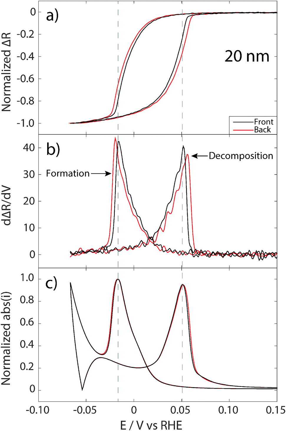 | ||
| Fig. 4 Normalized reflectance changes (a) from top (black curve) and bottom (red curve) for the hydride formation and decomposition on a 20 nm Pd film in 0.5 M H2SO4 with a scan rate of 5 mV s−1. The optical data represent wavelengths of 700 ± 5 nm. (b) The numerical derivative of the reflectance signal with respect to potential and for comparison the absolute current is shown in (c). The dashed gray lines represent the potential of maximum current (maximum global hydride formation/decomposition). | ||
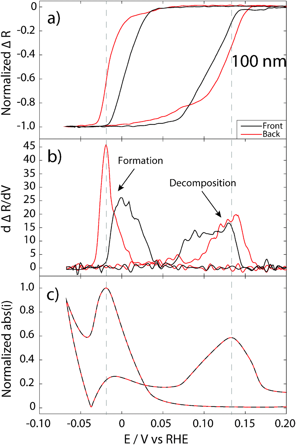 | ||
| Fig. 5 Normalized reflectance changes (a) from top (black curve) and bottom (red curve) for the hydride formation and decomposition on a 100 nm Pd film in 0.5 M H2SO4 with a scan rate of 5 mV s−1. The optical data represent wavelengths of 700 ± 5 nm. (b) The numerical derivative of the reflectance signal with respect to potential and for comparison the absolute current is shown in (c). The dashed gray lines represent the potential of maximum current (maximum global hydride formation/decomposition). | ||
The differences observed between front and back sides observed in Fig. 4a and b could, in principle, also be a result of restructuring of the Pd film after each cycle. To rule this out, we have plotted the absolute values of the simultaneously recorded current (Fig. 4c), which shows almost identical traces for the experiments with front and back reflectance. This means that the Pd film is virtually identical, and that the differences observed in the optical reflectance response obtained from the front and back sides indeed are related to the evolving asymmetric hydrogen concentration profile in the Pd film during hydrogen sorption/desorption. Thus, our measurements indicate that the hydride formation process starts and completes earlier at the interface towards the electrolyte, and thus closest to the proton supply. For the reverse process, hydride decomposition, it also completes earlier at the electrolyte interface and propagates into the film towards the support. It is also worth noting that the maximum in the current, for both independent measurements, coincides with the rate maximum obtained from the reflectance signal measured from the front. This further confirms that the time lag in rate maxima measured optically from the front and back sides indeed is a real effect related to hydrogen concentration gradients and not to different states of the sample in the two measurements.
The 100 nm Pd film is thicker than the optical skin depth of Pd. Thus, the optical fields irradiated from the front and back side do not penetrate the entire film. Therefore, it is possible to measure reflectance from the front and back side simultaneously, using the beam combiner device and, in contrast to the 20 nm film case, the respective beams only probe the interface closest to the irradiation source. For this constellation we observe large differences between the normalized reflectance signal measured from the front and from the back side. In the hydrogen sorption regime, both signals start to decrease at a potential of about 0.05 V and follow each other almost perfectly. This indicates that the incorporated H in the α-phase is very mobile and diffuses rapidly in the whole Pd volume and equilibrates the concentration, as expected. At more cathodic potentials, it is clear that the front-side reflectance starts to decrease earlier than the signal measured from back (Fig. 5a). This means that the formation of the β-phase starts at the free interface towards the electrolyte (and the supply of protons). Although this result is intuitive and agrees with the situation on 20 nm Pd, it is not obvious and as shown in a recent study by Baldi et al., the hydride formation can in some cases start at the opposite interface.40
It is now also interesting to look at the rate of hydride formation. The slopes of the normalized reflectance during formation measured from the front and from the back are very different, as can be seen in the derivative (Fig. 5b). The hydride formation rate is much higher at the back interface towards the support. This can be explained by a more or less stoichiometric PdHx phase formed in the upper part of the film (towards the electrolyte) propagated as a “front” towards the back of the film.
For the hydride decomposition in the 100 nm film, the situation is different. Clearly, the back-side reflectance signal starts to increase first, indicating that the hydride decomposition process starts at the back interface in this case. However, once the normalized reflectance signal measured from the front side also starts to increase, the two rate traces follow each other closely and reach the highest values at about the same potentials (Fig. 5b). This indicates that the hydride decomposition process is not simply the reverse of the formation and takes place with a quite homogenous H concentration throughout the entire Pd film.
For the 100 nm Pd film, the highest rate of reflectance change for both hydride formation and decomposition does not coincide with the maximum current (Fig. 5b and c), but occur later in time (at lower or higher potentials, respectively). This has to be interpreted as that the hydride formation and decomposition process is not homogeneous throughout the Pd film and that, in this case, the highest rate of hydride formation/decomposition at the interfaces does not occur at the same time as the highest rate of the total change in the film. One possible interpretation of this observation is that for this thick film, the stoichiometric hydride is first formed in the bulk of the film, away from the interfaces. The reason for this behavior might be related to different local lattice strain (e.g. compressive strain due to clamping to the support interface36,37) and microstructure (larger grains with fewer defects at the upper interface due to electrochemical conditioning of the surface – see Fig. 2), which gives rise to chemical potential gradients for hydride formation inside the film.
4. Conclusions
We have demonstrated an experimental setup that combines electrochemistry and fiber optics-based in situ UV/vis optical extinction and specular reflection spectroscopy. Using a beam combiner, for opaque films, simultaneous reflection measurements from the front and back side become possible. As a showcase, we have used this approach to examine electrochemical hydride and oxide formation in 20 and 100 nm thick Pd films as these are significantly thinner and thicker than the optical skin depth of Pd, respectively. Thus, on the 20 nm sample the specular reflectance signals measured at normal incidence from the front and back side of the glass-supported sample are very similar for both hydride and oxide formation. The reason is that the optical fields illuminated from both sides reach and probe both interfaces of the Pd film. Still we observed small differences in the temporal evolution of the reflectance changes measured from the front and from the back side, suggesting that both hydride formation and decomposition start at the front interface towards the electrolyte. Overall, the reflectance signals carry information very similar to the transmittance signal for the 20 nm Pd film.On the 100 nm Pd film, which is about two times thicker than the optical skin depth and thus opaque, transmittance measurements are impossible. However, the reflectance signals measured simultaneously from the front and back sides contain different and complementing information about the depth-evolution of the hydrogenation process. We find that the formation of the α-phase is homogeneous throughout the film whereas the formation of the β-phase starts at the free interface between the Pd film and the electrolyte and that it progresses at different rates close to the two film interfaces, compared to the global rate reflected in the current. The decomposition of PdHx starts at the backside of the film at the Pd–glass interface and progresses in a homogeneous fashion at the same rate in the entire film volume. As for hydrogen sorption, we find different decomposition rate maxima close to the sample interfaces compared to the global one in the current. As a reason for this behavior we suggest that the stoichiometric hydride is first formed in the bulk of the film, away from the interfaces, due to a different local lattice strain and microstructure situation, which gives rise to chemical potential gradients inside the film.
In summary, this work presents a simple, yet powerful way to analyze interactions of atomic and molecular species with a metal surface or volume in situ, in real time and with certain spatial resolution inside the film. Hence, it is relevant for numerous other processes beyond the demonstrated hydride formation model system, as for example the intercalation of ions in the electrodes of a battery, the formation/depletion of an alloy, or surface vs. bulk oxide formation.
Acknowledgements
BW thanks Formas (project number: 219-2011-959), JH, LF, NL, and CL the EU FP7's initiative Fuel Cell and Hydrogen Joint Undertaking's project CathCat (GA 303492), and CL the Swedish Research Council for financial support.Notes and references
- H. Baltruschat, J. Am. Soc. Mass Spectrom., 2004, 15, 1693–1706 CrossRef CAS PubMed.
- T. H. M. Housmans, A. H. Wonders and M. T. M. Koper, J. Phys. Chem. B, 2006, 110, 10021–10031 CrossRef CAS PubMed.
- Z. Jusys, J. Kaiser and R. J. Behm, Electrochim. Acta, 2002, 47, 3693–3706 CrossRef CAS.
- D. A. Buttry and M. D. Ward, Chem. Rev., 1992, 92, 1355–1379 CrossRef CAS.
- G. Jerkiewicz, G. Vatankhah, J. Lessard, M. P. Soriaga and Y.-S. Park, Electrochim. Acta, 2004, 49, 1451–1459 CAS.
- B. Wickman, H. Grönbeck, P. Hanarp and B. Kasemo, J. Electrochem. Soc., 2010, 157, B592–B598 CrossRef CAS PubMed.
- M. Łukaszewski and A. Czerwiński, J. Electroanal. Chem., 2006, 589, 87–95 CrossRef PubMed.
- Y. X. Chen, S. Ye, M. Heinen, Z. Jusys, M. Osawa and R. J. Behm, J. Phys. Chem. B, 2006, 110, 9534–9544 CrossRef CAS PubMed.
- T. Iwasita and F. C. Nart, Prog. Surf. Sci., 1997, 55, 271–340 CrossRef CAS.
- S. Gottesfeld, J. Electroanal. Chem., 1989, 15, 143–265 Search PubMed.
- S. Wagner, M. Moser, C. Greubel, K. Peeper, P. Reichart, A. Pundt and G. Dollinger, Int. J. Hydrogen Energy, 2013, 38, 13822–13830 CrossRef CAS PubMed.
- J. Kürschner, S. Wagner and A. Pundt, J. Alloys Compd., 2014, 593, 87–92 CrossRef PubMed.
- D. Friebel, D. J. Miller, C. P. O'Grady, T. Anniyev, J. Bargar, U. Bergmann, H. Ogasawara, K. T. Wikfeldt, L. G. M. Pettersson and A. Nilsson, Phys. Chem. Chem. Phys., 2011, 13, 262–266 RSC.
- E. S. Kooij, A. T. M. van Gogh and R. Griessen, J. Electrochem. Soc., 1999, 146, 2990–2994 CrossRef CAS PubMed.
- W. Lohstroh, R. J. Westerwaal, B. Noheda, S. Enache, I. Giebels, B. Dam and R. Griessen, Phys. Rev. Lett., 2004, 93, 197404 CrossRef CAS.
- R. Gremaud, C. P. Broedersz, D. M. Borsa, A. Borgschulte, P. Mauron, H. Schreuders, J. H. Rector, B. Dam and R. Griessen, Adv. Mater., 2007, 19, 2813–2817 CrossRef CAS PubMed.
- R. Gremaud, M. Slaman, H. Schreuders, B. Dam and R. Griessen, Appl. Phys. Lett., 2007, 91, 231916 CrossRef PubMed.
- B. M. Geerken, I. A. M. Corbiere and R. Griessen, J. Phys. Chem. Solids, 1983, 44, 793–799 CrossRef CAS.
- T. B. Flanagan and F. A. Lewis, Trans. Faraday Soc., 1959, 55, 1409–1420 RSC.
- M. Grdeń, M. Łukaszewski, G. Jerkiewicz and A. Czerwiński, Electrochim. Acta, 2008, 53, 7583–7598 CrossRef PubMed.
- G. Jerkiewicz, Prog. Surf. Sci., 1998, 57, 137–186 CrossRef CAS.
- N. Tateishi, K. Yahikozawa, K. Nishimura, M. Suzuki, Y. Iwanaga, M. Watanabe, E. Enami, Y. Matsuda and Y. Takasu, Electrochim. Acta, 1991, 36, 1235–1240 CrossRef CAS.
- F. A. Lewis, S. G. McKee and R. A. McNicholl, Z. Phys. Chem., 1993, 179, 63–68 CrossRef CAS.
- L. Birry and A. Lasia, Electrochim. Acta, 2006, 51, 3356–3364 CrossRef CAS PubMed.
- Y. Fukai, The Metal–Hydrogen System: Basic Bulk Properties, 2nd edn, Springer, 2005 Search PubMed.
- M. Łukaszewski and A. Czerwiński, J. Solid State Electrochem., 2011, 15, 2489–2522 CrossRef PubMed.
- H. Duncan and A. Lasia, Electrochim. Acta, 2008, 53, 6845–6850 CrossRef CAS PubMed.
- A. C. Switendick, J. Less-Common Met., 1987, 130, 249–259 CrossRef CAS.
- M. Ameen Poyli, V. M. Silkin, I. P. Chernov, P. M. Echenique, R. Díez Muiño and J. Aizpurua, J. Phys. Chem. Lett., 2012, 3, 2556–2561 CrossRef.
- W. E. Vargas, I. Rojas, D. E. Azofeifa and N. Clark, Thin Solid Films, 2006, 496, 189–196 CrossRef CAS PubMed.
- P. O. Nilsson and M. S. Shivaraman, J. Phys. C: Solid State Phys., 1979, 12, 1423–1427 CrossRef CAS.
- B. Wickman, T. J. Antosiewicz, J. Hagberg, J. Yan, A. Hellman and C. Langhammer, submitted manuscript.
- C. Gabrielli, P. P. Grand, A. Lasia and H. Perrot, J. Electrochem. Soc., 2004, 151, A1937–A1942 CrossRef CAS PubMed.
- J. K. Nørskov, T. Bligaard, A. Logadottir, J. R. Kitchin, J. G. Chen, S. Pandelov and U. Stimming, J. Electrochem. Soc., 2005, 152, J23–J26 CrossRef PubMed.
- R. Gremaud, M. Gonzalez-Silveira, Y. Pivak, S. de Man, M. Slaman, H. Schreuders, B. Dam and R. Griessen, Acta Mater., 2009, 57, 1209–1219 CrossRef CAS PubMed.
- Y. Pivak, R. Gremaud, K. Gross, M. Gonzalez-Silveira, A. Walton, D. Book, H. Schreuders, B. Dam and R. Griessen, Scr. Mater., 2009, 60, 348–351 CrossRef CAS PubMed.
- Y. Pivak, H. Schreuders, M. Slaman, R. Griessen and B. Dam, Int. J. Hydrogen Energy, 2011, 36, 4056–4067 CrossRef CAS PubMed.
- R. B. Schwarz and A. G. Khachaturyan, Acta Mater., 2006, 54, 313–323 CrossRef CAS PubMed.
- M. Łukaszewski and A. Czerwiński, J. Electroanal. Chem., 2006, 589, 38–45 CrossRef PubMed.
- A. Baldi, M. Gonzalez-Silveira, V. Palmisano, B. Dam and R. Griessen, Phys. Rev. Lett., 2009, 102, 226102 CrossRef CAS.
Footnote |
| † Electronic supplementary information (ESI) available: Wavelength dependence of optical response and H/Pd quantification. See DOI: 10.1039/c5cp01339a |
| This journal is © the Owner Societies 2015 |