
Trade-offs of the opto-electrical properties of a-Si:H solar cells based on MOCVD BZO films
Ze
Chen
,
Xiao-dan
Zhang
*,
Jun-hui
Liang
,
Jia
Fang
,
Xue-jiao
Liang
,
Jian
Sun
,
De-kun
Zhang
,
Xin-liang
Chen
,
Qian
Huang
and
Ying
Zhao
Institute of Photo Electronic Thin Film Devices and Technology of Nankai University, Key Laboratory of Photoelectronic Thin Film Devices and Technology, Tianjin 300071, P. R. China. E-mail: xdzhang@nankai.edu.cn; Fax: +86 22-23499304; Tel: +86-22-23499304
First published on 22nd October 2014
Abstract
Boron-doped zinc oxide (BZO) films, deposited by metal–organic chemical vapor deposition (MOCVD), have been widely used as front electrodes in thin-film solar cells due to their native pyramidal surface structure, which results in efficient light trapping. This light trapping effect can enhance the short-circuit current density (Jsc) of solar cells. However, nanocracks or voids in the silicon active layer may form when the surface morphology of the BZO is too sharp; this usually leads to degraded electrical properties of the cells, such as open-circuit voltage (Voc) and the fill factor (FF), which in turn decreases efficiency (Eff) [Bailat et al., Photovoltaic Energy Conversion, Conference Record of the 2006 IEEE 4th World Conference on. IEEE, 2006, vol. 2, pp. 1533–1536]. In this paper, an etching and coating method was proposed to modify the sharp “pyramids” on the surface of the BZO films. As a result, an evident enhancement was achieved for these modified, BZO-based cells' Voc, FF, and Eff, although the Jsc exhibited a small decrease. In order to increase the Jsc and maintain the improved electrical properties (Voc, FF) of the cell, a thin BZO coating, deposited by MOCVD, was introduced to coat the sputtering-treated BZO film. Finally, we optimized the trade-off among the Voc, FF, and Jsc, that is, we identified a regime with an increase of the Jsc as well as a further improvement of the other electrical properties.
1. Introduction
The light-induced degradation effect2,3 in hydrogenated amorphous silicon (a-Si:H) thin-film solar cells becomes obvious when the active layer is thick. Light trapping is of great importance in enlarging the light path in solar cells and reducing active-layer thickness as well as overall cost. Among the types of transparent conductive oxide (TCO) films used as front electrodes, pyramidal boron-doped zinc oxide (BZO) film, fabricated by metal organic chemical vapor deposition (MOCVD), has been successfully used in thin-film silicon solar cells with record performance.4,5 As an effect of their natively pyramidal surface morphology, BZO films exhibit favorable light-trapping capacity.6–8 However, their overly sharp pyramidal surface features may lead to nanocracks or voids in subsequently deposited layers required for thin-film solar cells,9,10 which may worsen their open-circuit voltage (Voc) and fill factor (FF).Researchers have made several efforts to determine how to improve the electrical properties of such solar cells. Dominé,11 Bailat,1 and Addonizio12 have used N2, O2, or Ar plasma to treat BZO films, and have achieved an ideal modification of the surface features as well as obvious improvements of the Voc and FF of BZO-based thin-film solar cells. Boccard13 and Söederströem14 have used multilayers to improve the electrical properties of such cells without negatively affecting the TCO's light trapping capacity. Additionally, Bancha Janthong15 and Aswin Hongsingthong16 have deposited smaller-size pyramidal BZO films on etched rough glass substrates to produce a new, cauliflower-like surface morphology.
In this study, we developed a new method for enhancing the opto-electrical properties of a-Si:H thin-film solar cells. Firstly, we deposited the pyramidal BZO film using MOCVD to produce a high surface root-mean-square roughness (RMS) of about 60–80 nm. Then, we used a magnetron-sputtering system to treat the MOCVD–BZO films. The high-energy-sputtering, hydrogen-doped ZnO (HZO) molecules successfully etched the sharp “pyramids” and covered the surface of the BZO with a thin HZO film. Lastly, we added a thin BZO film with smaller pyramids using MOCVD on the surface of the sputtering-treated BZO film to balance the opto-electrical properties of the thin-film a-Si:H solar cell.
2. Experimental details
For this study, 3 μm thick bottom-layer BZO films were fabricated on glass substrates (Corning Eagle XG) using MOCVD. Diethylzinc and H2O vapor were used as the precursors with flow rates of 180 sccm and 110 sccm, respectively. In addition, borane was used as a doping gas. The doping processes were 3 sccm (3 min) + 0 sccm (32 min) + 3 sccm (15 min) and 3 sccm (3 min) + 0 sccm (32 min) + 2 sccm (15 min), for the bottom BZO films in Fig. 2(a) and 3(a) respectively. The thin, top-layer BZO films were also doped continuously in 3 sccm. The growth temperature was kept at approximately 423 K, and the pressure in the deposition reactor was 0.02 Torr. We etched the standard BZO films using a pulsed direct-current magnetron-sputtering system with a pure, sintered ceramic ZnO target. H2 was used as the doping source and the deposition power was set to 340 W. After the sputtering process, the bottom BZO film was etched and coated with a sputtered film of ZnO:H. Then, 100–500 nm top-layer BZO films were deposited on the etched BZO films, also by MOCVD.We used a radio-frequency, plasma-enhanced chemical vapor deposition (RF-PECVD) cluster system to fabricate PIN-type single-junction a-Si:H solar cells on these TCO films, with a growth temperature of approximately 483 K. The intrinsic Si layer, with a thickness of 250 nm, was deposited using a mixture of hydrogen and silane. The p- and n-type layers were produced by adding trimethylboron (TMB) and phosphine (PH3), respectively. SiOx films were then prepared by adding carbon dioxide (CO2). Lastly, a ZnO/Ag film was used as a back reflector. The cells' structure is shown in Fig. 1.
 | ||
| Fig. 1 Structure of an a-Si:H solar cell. | ||
The surface morphologies of the TCO films were characterized using atomic force microscopy (AFM) (SPA 400, Seiko) and scanning electron microscopy (SEM) (Supra550p, Zeiss). The total reflectance (TR) and total and direct optical transmittances (TT and DT, respectively) of the TCO films, as well as the TR values of the fabricated a-Si:H solar cells were measured using an ultraviolet-visible-near-infrared (UV-Vis-NIR) spectrophotometer (Cary 5000 PC, Varian). The performance of the a-Si:H solar cells was determined from their current density versus voltage (J–V) characteristics, which were obtained using an AM1.5 solar simulator (WXS-156S-L2, Wacom). The external quantum efficiencies (EQEs) of the cells were determined under the short-circuit conditions for wavelengths ranging from 300 nm to 800 nm. All of these measurements were made at room temperature.
3. Results and discussion
BZO films used in this study were deposited by MOCVD—a representative SEM surface image is shown in Fig. 2(a) as an inset. Clearly, the surface of the standard BZO film consists of pyramids with sharp tips and flat sides. Thus, we employed a magnetron-based sputtering method to smooth the sharp features. The sputtered hydrogen-doped ZnO (HZO) molecules arrived at the surface of the BZO film with high kinetic energy, etched the sharp tips of the pyramidal features, and simultaneously formed a HZO–BZO film (Fig. 2(a)). As we can see from the SEM image of the treated BZO, the sharp edges of the pyramids were smoothed, that is, most of the sharp tips vanished.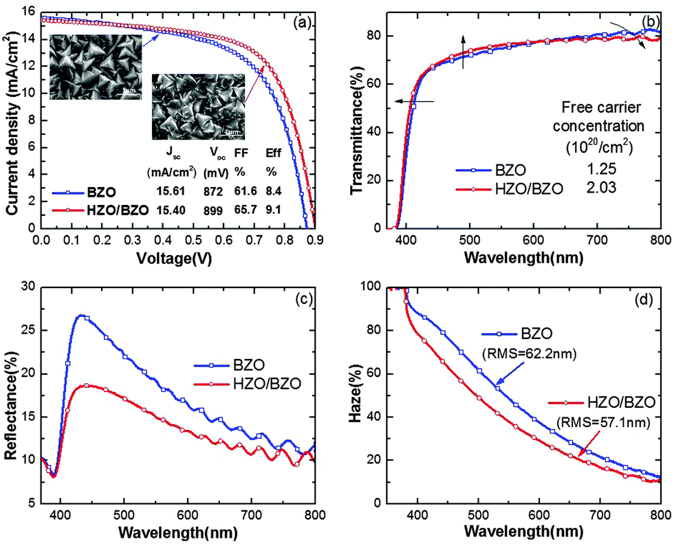 | ||
| Fig. 2 (a) J–V curves for the a-Si:H solar cells based on BZO and HZO–BZO films. (b) Total transmittance, (c) reflectance and (d) haze curves of the BZO and HZO–BZO films. | ||
Then, we deposited single-junction a-Si:H solar cells on these TCO films to verify whether such modification is suitable for improving the electrical properties of the cells. The corresponding J–V curves are shown in Fig. 2(a). Solar cells based on the HZO–BZO film exhibited a clear increase in Voc and FF owing to the smooth surface morphology, which mainly resulted from the modified surface forming fewer nanocracks in the silicon active layer8,11,17 (the diode quality factor n decreased from 1.87 to 1.78). For a-Si:H solar cells, the value of the diode quality factor n (which describes the cells' quality) was 1–2. This suggests that the bulk recombination of the carriers worsened when the value was closer to 2. After the sputtering treatment, the smaller pyramidal features vanished by the etching effect. As a result, the carrier mobility increased from 14.1 to 17.4 cm2 V−1 s−1, owing to the decreased grain boundary density. In addition, there may be diffusion of hydrogen atoms in the BZO grain boundaries, which would also improve the carrier mobility by decreasing its recombination. Once coated by the HZO film, the treated TCO film had a lower sheet resistance (reduced from 21.8 to 18.21 Ω sq−1). Moreover, the cells' series resistance (Rs) decreased from 7.24 to 6.96 Ω cm2 and their shunt resistance (Rsh) increased from 601 to 1140 Ω cm2. Thus, we achieved a final gain in efficiency as a result of the improvement of the Voc and FF, though the Jsc decreased slightly.
This decrease in Jsc can be explained in terms of the measured optical properties of these two TCO films. The total transmittance and reflectance of the standard and treated BZO films are shown in Fig. 2(b) and (c), respectively. The HZO layer covers the bottom BZO film after the sputtering process. Doping of hydrogen caused the treated BZO film to exhibit a higher free-carrier concentration, which resulted in a broadened bandgap and a blue shift of the transmittance curve (Fig. 2(b)).18,19 Because of the surface modification,20 the reflectance of the HZO–BZO film decreased considerably in the 400–600 nm range (Fig. 2(c)). This decreased reflectance led to a slight enhancement in transmittance. Meanwhile, the increased free-carrier concentration resulted in a higher free-carrier absorption (FCA) effect,7,21 particularly in the long-wavelength region. Thus, the total transmittance curves of the treated BZO film decreased at wavelengths greater than 600 nm.
Because the surface morphology was smoothed and the surface RMS decreased (Fig. 2(d)) after this modification, a decay of the TCO's scattering capacity was observed. As a result, the haze factor of the TCO film showed an evident reduction after the sputtering treatment. Though the transmittance curve slightly increased at wavelengths shorter than 600 nm, the actual uptake of light, as well as Jsc, was reduced due to this clearly diminished haze factor.
From the above experiments, we achieved an improvement of Voc and FF at the cost of a decrease in Jsc. In an attempt to increase the cells' Jsc and simultaneously maintain favorable electrical properties, we deposited a series of thin BZO films, with thicknesses of 100–500 nm, on the surface of the HZO–BZO films to impose a new light-trapping morphology. Considering that the light-scattering capacity of BZO films increases with increasing surface RMS, we slightly decreased the doping level to achieve a rougher bottom-layer BZO film. This BZO film had a lower free-carrier concentration and similar optical properties to that in Fig. 2(b)–(d), and was subsequently modified using sputtering, then coated by a thin, top-layer BZO film.
SEM images of the BZO–HZO–BZO films with this refined morphology are shown in Fig. 3. After applying a top-layer BZO film of about 100 nm thickness, most of the sharp tips of the pyramids smoothed by the sputtering treatment re-formed (Fig. 3(c)). This occurred mainly because the sputtered HZO molecules arrived at the surface of the pyramids and smoothed their tips, and then had priority to travel into the “valleys” instead of staying on the smoothed tops. As a result, the top BZO grew along the bottom BZO film and re-sharpened its smoothed tips. Because of the accumulation of HZO in these valleys between pyramids, the thin, top-layer BZO film provided extremely small features on the sides or bottoms of the pyramids, and the surface RMS of the BZO–HZO–BZO films decreased. Increasing the thickness of the top BZO film to 300 nm, these very small features in the valleys expanded to form a series of pyramidal features. When the top BZO film was deposited at a thickness of 500 nm, the smaller pyramidal features continuously expanded to form larger features between the large bottom pyramids.
 | ||
| Fig. 3 SEM images of the (a) BZO and (b) HZO–BZO films and the BZO–HZO–BZO films coated by a top-layer BZO with thicknesses of (c) 100 nm, (d) 300 nm, and (e) 500 nm. | ||
To clearly elucidate the changes in surface morphology, we also acquired the cross-sectional AFM images of the TCO films. Recalling that the sputtering HZO bombarded the sharp tips and covered the valleys of the pyramidal BZO surface features, the largest depth between tips and valleys (ΔZ) after this process decreased from 329 nm (Fig. 4(a)) to 267 nm (Fig. 4(b)). Then, the top BZO film restored the tips of the bottom BZO film and formed small pyramidal features to fill up the valleys (Fig. 4(c)–(e)). The combination of the restored large bottom pyramidal features and the small top pyramids in the valleys caused the surface to change to a more smoothed “U” type from the sharp “V” type (Fig. 4(e)).
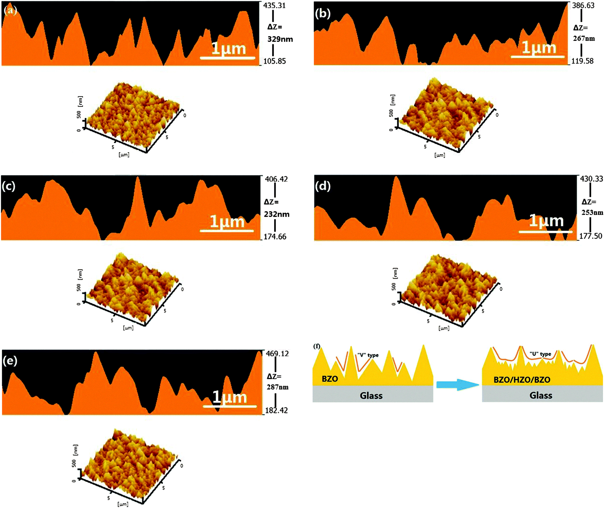 | ||
| Fig. 4 Cross-sectional and 3-dimensional AFM images of the (a) BZO, (b) HZO–BZO, (c) BZO(100 nm)–HZO–BZO, (d) BZO(300 nm)–HZO–BZO, (e) BZO(500 nm)–HZO–BZO, and a sketch of the surface changes (f). | ||
In addition, the deposition of the thin, top-layer BZO film also improved the TCOs' electrical properties (Table 1). When we increased the thickness of the top BZO film, there was an increase of free-carrier concentration and decrease of sheet resistance due to the continuously increasing B2H6 doping. When coated by a 100 nm thick BZO film, the grain-boundary density may have increased because of the recovery of the small size features, which slightly decreased mobility. However, with the increasing thickness of the top BZO film, the regrowth of the bottom BZO grains, enlargement of the new top features, and the resulting increase of free-carrier concentration would enhance the carrier mobility of the TCO film.
| Thickness of top BZO film | BZO | 0 nm | 100 nm | 300 nm | 500 nm |
|---|---|---|---|---|---|
| RMS (nm) | 86.6 | 71.8 | 73.9 | 74.8 | 77.8 |
| Free carrier concentration (1020 cm−2) | 1.36 | 1.20 | 1.51 | 1.68 | 1.74 |
| Charge carrier mobility (cm2 V−1 s−1) | 22.7 | 32.1 | 29.5 | 32.9 | 35.6 |
| R sh (Ω cm2) | 733 | 760 | 1061 | 1497 | 950 |
| R s (Ω cm2) | 6.20 | 5.87 | 5.83 | 5.67 | 5.36 |
| Sheet resistance (Ω sq−1) | 20.22 | 16.21 | 14.05 | 10.91 | 10.43 |
Next, we deposited a-Si:H solar cells on these BZO and BZO(0–500 nm)–HZO–BZO substrates to check whether the treatment is beneficial for improving the cells' Jsc and electrical properties. From the J–V curves of these cells in Fig. 6, we found that the Jsc achieved an ideal gain with increasing top-BZO thickness. We evaluated the actual light uptake by measuring the absorption (Fig. 5(b)) of the TCO films and solar cells. As the free-carrier concentration of the samples increased (Table 1) with the thickness of the top BZO film, the total transmittance and absorption curves of the TCO films exhibited major differences (Fig. 5(a)). It should be noted that the total transmittance curves were measured in air, and some light might be totally reflected at the TCO/air interface instead of being measured by the collector. Additionally, the combined small, top pyramidal features and large bottom pyramids may lead to the formation of a gradient refractive index in the cells, and, in turn, a decreased reflectance. As a result, the absorption properties of the cells based on these samples were similar for 300–600 nm light, even though the total transmittance behaved differently. At wavelengths greater than 600 nm, the cells' absorption increased with increasing top-BZO thickness. We may also attribute the aforementioned Jsc gain to this increasing absorption in the 600–800 nm wavelength region.
 | ||
| Fig. 5 (a) Total transmittance and (b) absorption curves of the samples. | ||
Since the combined regrowth of the bottom BZO and deposition of small pyramidal top BZO film induced a smoothed “U”-type morphology, which benefited in reducing the nanocracks or voids in the cells (the diode quality factor n decreased from 1.86 to 1.52), the Voc and FF of the cells were improved further with increasing top-BZO thickness (0–300 nm) (Fig. 6). In addition, the deposition of the top BZO film improved the TCO's electrical properties and reduced the Rs of the cells, which also enhanced the FF. Owing to the decrease of Rsh with the top-BZO thickness at 500 nm, the FF did not improve further (though the Rs decreased). Unfortunately, when we increased the top-BZO thickness to 500 nm, the return of the sharp tips, and especially the overgrowth of the smaller features impaired the Voc and FF properties, though the Jsc still achieved a gain. As a result, the efficiency of cells based on the BZO–HZO–BZO substrate could not be improved further for top-BZO thicknesses larger than 300 nm.
 | ||
| Fig. 6 J–V curves of the a-Si:H solar cells based on BZO and BZO(0–500 nm)–HZO–BZO films. | ||
4. Conclusions
In this paper, we attempted to balance the trade-offs of the opto-electrical properties of a-Si:H solar cells by using a sputtered ZnO:H coating to modify a pyramidal BZO film. Then, we produced a suitably modified BZO film to improve the cells' Voc and FF by 3.2% and 6.5%, respectively. The efficiency of the cell based on this HZO–BZO film was improved, though the Jsc decreased as a result. To remedy this without impairing the Voc and FF of the cells, we added a thin, top-layer BZO film to form a “U”-type surface morphology. By increasing the top-BZO thickness from 100 nm to 500 nm, we achieved a continuous increase of the Jsc but a decrease of Voc and FF for thicknesses greater than 300 nm. Thus, a suitable top BZO (thickness of 300 nm) has been shown to improve a standard BZO cell's light trapping and electrical properties.Acknowledgements
The authors gratefully acknowledge support from National Basic Research Program of China (Grant No. 2011CBA00706 and 2011CBA00707), the Science and Technology Support Program of Tianjin (12ZCZDGX03600), the Major Science and Technology Support Project of Tianjin City (11TXSYGX22100), and the Specialized Research Fund for the PhD Program of Higher Education (20120031110039).References
- J. Bailat, D. Dominé, R. Schlüchter, J. Steinhauser, S. Faÿ, F. Freitas, C. Bücher, L. Feitknecht, X. Niquille, T. Tscharner, A. Shah, C. Ballif, High-efficiency pin microcrystalline and micromorph thin film silicon solar cells deposited on LPCVD ZnO coated glass substrates[C]. Photovoltaic Energy Conversion, Conference Record of the 2006 IEEE 4th World Conference on. IEEE, 2006, vol. 2, pp. 1533–1536.
- S. Nicolay, M. Despeisse, F.-J. Haug and C. Ballif, Control of LPCVD ZnO growth modes for improved light trapping in thin film silicon solar cells, Sol. Energy Mater. Sol. Cells, 2011, 95, 1031–1034 CrossRef CAS PubMed.
- G. Yue, L. Sivec, J. M. Owens, B. Yan, J. Yang and S. Guha, Optimization of back reflector for high efficiency hydrogenated nanocrystalline silicon solar cells, Appl. Phys. Lett., 2009, 95, 263501 CrossRef PubMed.
- S. Faÿ, L. Feitknecht, R. Schlüchter, U. Kroll, E. Vallat-Sauvain and A. Shah, Rough ZnO layers by LP-CVD process and their effect in improving performances of amorphous and microcrystalline silicon solar cells, Sol. Energy Mater. Sol. Cells, 2006, 90, 2960–2967 CrossRef PubMed.
- S. Nicolay, M. Benkhaira, L. Ding, J. Escarre, G. Bugnon, F. Meillaud and C. Ballif, Control of CVD-deposited ZnO films properties through water/DEZ ratio: decoupling of electrode morphology and electrical characteristics, Sol. Energy Mater. Sol. Cells, 2012, 105, 46–52 CrossRef CAS PubMed.
- S. Faÿ, U. Kroll, C. Bucher, E. Vallat-Sauvain and A. Shah, Low pressure chemical vapour deposition of ZnO layers for thin-film solar cells: temperature-induced morphological changes, Sol. Energy Mater. Sol. Cells, 2005, 86, 385–397 CrossRef PubMed.
- S. Faÿ, J. Steinhauser, N. Oliveira, E. Vallat-Sauvain and C. Ballif, Opto-electronic properties of rough LP-CVD ZnO: B for use as TCO in thin-film silicon solar cells, Thin Solid Films, 2007, 515, 8558–8561 CrossRef PubMed.
- S. Faÿ, J. Steinhauser, S. Nicolay and C. Ballif, Polycrystalline ZnO:B grown by LPCVD as TCO for thin film silicon solar cells, Thin Solid Films, 2010, 518, 2961–2966 CrossRef PubMed.
- M. Python, O. Madani, D. Dominé, F. Meillaud, E. Vallat-Sauvain and C. Ballif, Influence of the substrate geometrical parameters on microcrystalline silicon growth for thin-film solar cells, Sol. Energy Mater. Sol. Cells, 2009, 93, 1714–1720 CrossRef CAS PubMed.
- J. Meier, S. Dubail, S. Golay, U. Kroll, S. Faÿ, E. Vallat-Sauvain, L. Feitknecht, J. Dubail and A. Shah, Microcrystalline silicon and the impact on micromorph tandem solar cells, Sol. Energy Mater. Sol. Cells, 2002, 74, 457–467 CrossRef CAS.
- D. Dominé and C. Ballif, The role of front electrodes and intermediate reflectors in the optoelectronic properties of high-efficiency micromorph solar cells [D], Université de Neuchâtel, 2009 Search PubMed.
- M. L. Addonizio and A. Antonaia, Surface morphology and light scattering properties of plasma etched ZnO:B films grown by LP-MOCVD for silicon thin film solar cells, Thin Solid Films, 2009, 518, 1026–1031 CrossRef CAS PubMed.
- M. Boccard, C. Battaglia, S. Hänni, K. Söderström, J. Escarré, S. Nicolay, F. Meillaud, M. Despeisse and C. Ballif, Multiscale Transparent Electrode Architecture for Efficient Light Management and Carrier Collection in Solar Cells, Nano Lett., 2012, 12, 1344–1348 CrossRef CAS PubMed.
- K. Söederströem, G. Bugnon, F.-J. Haug, S. Nicolay and C. Ballif, Experimental study of flat light-scattering substrates in thin-film silicon solar cells, Sol. Energy Mater. Sol. Cells, 2012, 101, 193–199 CrossRef PubMed.
- B. Janthong, Y. Moriya, A. Hongsingthong, P. Sichanugrist and M. Konagai, Management of light-trapping effect for a-Si:H/mc-Si:H tandem solar cells using novel substrates, based on MOCVD ZnO and etched white glass, Sol. Energy Mater. Sol. Cells, 2013, 119, 209–213 CrossRef CAS PubMed.
- A. Hongsingthong, L. Zhang, I. A. Yunaz, S. Miyajima, M. Konagai, Multi-layer ZnO films with high haze ratio for use as front TCO in Si-based thin film solar cells, 25th European Photovoltaic Solar Energy Conference and Exhibition/5th World Conference on Photovoltaic Energy Conversion, 6–10 September 2010, Valencia, Spain.
- G. Bugnon, High-Quality Microcrystalline Silicon for Efficient Thin-Film Solar Cells: Insights into Plasma and Material Properties [D], Cole Polytechnique Fédérale De Lausanne, 2013 Search PubMed.
- L. Gong, J. Lu and Z. Ye, Transparent and conductive Ga-doped ZnO films grown by RF magnetron sputtering on polycarbonate substrates, Sol. Energy Mater. Sol. Cells, 2010, 94, 937–941 CrossRef CAS PubMed.
- C. E. Kim, P. Moon, S. Kim, J.-M. Myoung, H. W. Jang, J. Bang and I. Yun, Effect of carrier concentration on optical bandgap shift in ZnO:Ga thin films, Thin Solid Films, 2010, 518, 6304–6307 CrossRef CAS PubMed.
- Y. T. Chae, J. Kim, H. Park and B. Shin, Building energy performance evaluation of building integrated photovoltaic (BIPV) window with semi-transparent solar cells, Appl. Energy, 2014, 129, 217–227 CrossRef CAS PubMed.
- L. Ding, M. Boccard, G. Bugnon, M. Benkhaira, S. Nicolay, M. Despeisse, F. Meillaud and C. Ballif, Highly transparent ZnO bilayers by LP-MOCVD as front electrodes for thin-film micromorph silicon solar cells, Sol. Energy Mater. Sol. Cells, 2012, 98, 331–336 CrossRef CAS PubMed.
| This journal is © the Owner Societies 2015 |