
Strong temperature-dependent crystallization, phase transition, optical and electrical characteristics of p-type CuAlO2 thin films
Suilin
Liu
ab,
Zhiheng
Wu
ab,
Yake
Zhang
ab,
Zhiqiang
Yao
*ab,
Jiajie
Fan
ab,
Yiqiang
Zhang
ab,
Junhua
Hu
ab,
Peng
Zhang
ab and
Guosheng
Shao
abc
aSchool of Materials Science and Engineering, Zhengzhou University, Zhengzhou 450001, P.R. China. E-mail: zqyao@zzu.edu.cn
bInternational Joint Research Laboratory for Low-Carbon & Environmental Materials of Henan Province, Zhengzhou University, Zhengzhou 450001, Henan, P.R. China
cInstitute for Renewable Energy and Environmental Technologies, University of Bolton, Bolton BL3 5AB, UK
First published on 5th November 2014
Abstract
We report here a reliable and reproducible single-step (without post-annealing) fabrication of phase-pure p-type rhombohedral CuAlO2 (r-CuAlO2) thin films by reactive magnetron sputtering. The dependence of crystallinity and phase compositions of the films on the growth temperature was investigated, revealing that highly-crystallized r-CuAlO2 thin films could be in situ grown in a narrow temperature window of ∼940 °C. Optical and electrical property studies demonstrate that (i) the films are transparent in the visible light region, and the bandgaps of the films increased to ∼3.86 eV with the improvement of crystallinity; (ii) the conductance increased by four orders of magnitude as the film was evolved from the amorphous-like to crystalline structure. The predominant role of crystallinity in determining CuAlO2 film properties was demonstrated to be due to the heavy anisotropic characteristics of the O 2p-Cu 3d hybridized valence orbitals.
Introduction
Transparent oxide electronics is one of the most advanced topics for a wide range of device applications, and to achieve stable and reliable wide bandgap oxide semiconductors (WBOSs) with controllable carrier concentration and conduction type is a long-lasting research focus.1–4 Thus far, significant progress has been accomplished in synthesis, conductivity control and device applications of n-type WBOSs, such as In, Ga, Zn, Sn-based binary or multicomponent oxides.5–7 Thin film transistors based on an amorphous InGaZnO4 channel layer have been commercialized as the ideal replacements of a-Si and/or LTPS (low temperature poly-silicon) for pixel-switching in ultrahigh-resolution (UHD 4 K) flat-panel displays, tablets and smartphones. However, it has been illustrated that the WBOSs are in general characteristic with deep valence band maximums (VBMs) around 7.0–8.0 eV (e.g., TiO2 ∼ 7.6 eV, ZnO ∼ 8.1 eV), and their VBMs are composed of strong localized O 2p6 orbitals with large electronegativity.8 Meanwhile, unintentional defects (oxygen vacancies) are easily formed in such oxides, which behave as donors (hole killers) and thus compensate acceptors. Therefore, it is difficult to realize effective hole doping and to obtain a stable and high hole mobility.3,4,9–11 For instance, N-doped ZnO films grown by molecular-beam epitaxy with a temperature modulation technique exhibit p-type conduction with, however, a low hole mobility (∼5–8 cm2 V−1 s−1) and a high donor compensation ratio (ND/NA ∼ 0.8).12Delafossite CuAlO2 shows intrinsic p-type conduction owing to the lower formation energies of acceptors (e.g. copper vacancies and interstitial oxygen) compared to donors (e.g. oxygen vacancies and interstitial copper).13–16 It has a wide bandgap (>3.5 eV), and its VBM is dominated by a large hybridization of the oxygen orbitals with 3d10 electrons in the Cu1+ closed shell, which reduces the contribution due to oxygen orbitals and leads to a dispersive valence band (low effective mass).17,18 The discovery of p-type electrical conduction in transparent thin films of CuAlO2 is recognized as a milestone forward since it provides a mechanism for equilibrium p-type conduction free from self-compensation, superior to the conventional p-type WBOSs. It is interesting to note that more than 600 following studies have been devoted to addressing the preparation and electrical property modulation of CuAlO2 since this novel material was developed. However, only limited success has been achieved to date, and it is still problematic to synthesize highly crystalline and phase-pure r-CuAlO2 films. CuAlO2 tends to decompose into CuAl2O4 and CuO phases at ∼1003 °C via 4CuAlO2 + O2 → 2CuAl2O4 + 2CuO.19 Generally, the CuAlO2 films, prepared by both physical and chemical deposition techniques, show poor crystallinity and phase purity. Post-annealing at a high temperature for its equilibrium existence (∼1000–1100 °C) was indispensably adopted to improve the crystal quality, which however induced uncontrollable impurity phases such as Cu2O, CuO, CuAl2O4 and Al2O3.19–30 Such a situation impedes many critical technological developments.
Thus, in this work, we report a reliable and reproducible single-step approach to grow highly crystallized rhombohedral CuAlO2 (R![[3 with combining macron]](https://www.rsc.org/images/entities/char_0033_0304.gif) m) films by reactive magnetron sputtering, and demonstrate in particular the influence of growth temperature on the crystallization and phase transition behavior of Cu–Al–O thin films. The optical and electrical properties of the CuAlO2 films are verified to be highly sensitive to the film crystallinity, which is ascribed to the heavy anisotropic characteristics of the O 2p-Cu 3d hybridized valence orbitals in r-CuAlO2 films.
m) films by reactive magnetron sputtering, and demonstrate in particular the influence of growth temperature on the crystallization and phase transition behavior of Cu–Al–O thin films. The optical and electrical properties of the CuAlO2 films are verified to be highly sensitive to the film crystallinity, which is ascribed to the heavy anisotropic characteristics of the O 2p-Cu 3d hybridized valence orbitals in r-CuAlO2 films.
Experimental
Cu–Al–O films were deposited on 100 nm SiO2 coated n-Si wafers by radio frequency (RF) reactive magnetron sputtering (ION'X®, Germany) using a 4 inch Cu0.42Al0.58 alloy target (purity 99.999%). The reactive RF sputtering was performed at a working pressure of 2.0 × 10⁻³ mbar, oxygen and argon flow rates of 16 and 4 SCCM (SCCM denotes standard cubic centimeter per minute), respectively. The target-to-substrate distance was fixed at ∼6 cm. The samples were in situ heated using a 1200 °C high temperature O2 compatible heater (HeatWave Labs, USA). The substrate temperatures were probed by an Omega K-type thermocouple contacted with the sample's back surface. The forward RF power was 120 W, and the corresponding dc self-bias potentials were measured to be −210 V. After deposition, the samples were cooled down at a speed of less than 30 °C min−1 accompanied by oxygen gas protection.Phase structures of the samples were analyzed by X-ray diffraction (XRD, PANalytical X'pert pro MPD) and Fourier transform infrared spectroscopy (FT-IR, Nicolet 6700). The chemical composition of the films was investigated by X-ray photoelectron spectroscopy (XPS) using an Axis Ultra DLD spectrometer (Kratos Analytical, UK). The film morphologies and element concentration were observed using a Philips XL30 FEG field-emission scanning electron microscope (FESEM) attached with the energy dispersive X-ray (EDX) spectrometer. The crystallinity and microstructure of the r-CuAlO2 films were examined using a Philips CM200 FEG high-resolution transmission electron microscope (HRTEM). UV-Vis absorption spectra were recorded using Perkin Elmer Lambda 750 UV-Vis spectrophotometer. The electrical properties were measured using an AC field Hall measurement system in the Van der Pauw geometry (LakeShore 84030). It extends Hall mobility measurement capabilities down to 0.001 cm2 V−1 s−1, allowing us to measure the low mobility materials with far greater resolution.
Results and discussion
Fig. 1(a) shows the θ − 2θ XRD patterns of Cu–Al–O films grown at different substrate temperatures ranging from 800 to 1000 °C. Interestingly, however, broad and weak Bragg's peaks with an amorphous-like background were found in the case of the film grown at 800 °C (denoted as sample F1), suggesting a poor crystallinity nature of the corresponding film. As the substrate temperature increases to 870 °C (F2) and 940 °C (F3), the crystallinity of the films is improved drastically, evidenced by the sharp and intense diffraction peaks. Nonetheless, further increasing the temperature to ∼1000 °C (F4) results in broadening of the diffraction peaks, which was considered to be due to the following reactions occurring at elevated temperature:| 4CuAlO2 + O2 → 2CuAl2O4 + 2CuO | (1) |
| 4CuAl2O4 → 4CuAlO2 + 2Al2O3 + O2 | (2) |
The formation of CuO phases was also confirmed by the intense peaks centered at ∼560 cm−1 corresponding to the stretching vibration of Cu–O in the FT-IR spectra shown in Fig. 1(b).31,32 The indexing of the XRD diffraction peaks reveals that samples F1, F2 and F4 are mixtures of CuAlO2, CuO and CuAl2O4 phases, and sample F3 is composed of single delafossite CuAlO2. The high crystallinity and phase purity of sample F3 are also supported by the sharp FT-IR peak centered at 856 cm−1 and the narrow full width at half maximum (FWHM). The above observations illustrate that both the crystallinity and the phase composition of the Cu–Al–O films are highly temperature dependent. Delafossite CuAlO2 films with high crystallinity and phase-purity could be grown within a narrow temperature window of ∼940 °C. The crystallinity of the films grown at elevated temperature by the single-step process is significantly improved as compared with the previous reports which yielded poor crystallinity and impurity phases such as Cu2O, CuAl2O4, Al2O3 and CuO.19–30
 | ||
| Fig. 1 (a) XRD patterns and (b) FTIR images of the Cu–Al–O films grown at substrate temperatures of 800 °C (F1), 870 °C (F2), 940 °C (F3) and 1000 °C (F4). | ||
The phase evolution with respect to the growth temperature for CuAlO2 is considered to be controlled by the thermodynamic characteristics of CuAlO2, CuAl2O4, Cu2O and CuO phases. It is important to note that, under equilibrium conditions in air, CuAlO2 can only be thermodynamically stable in a narrow temperature range of 1003–1250 °C. Moreover, three phase boundaries, i.e. CuAl2O4 + CuAlO2, CuAlO2 + Cu2O, CuAlO2 + CuO, are identified at around 1160 °C, 1140 °C and 1020 °C in such a narrow temperature window, respectively.19 This diagram clearly suggests that highly crystallized and phase-pure r-CuAlO2 films should (could only) be fabricated in an extremely narrow temperature window, in addition, with proper chemical configurations. Thus, it is important to investigate the chemical composition of as-deposited films, which are responsible for the formation of different phases.
Fig. 2 depicts the (a–d) plane- and (e–h) tilt-view FESEM images of the Cu–Al–O films (samples F1–F4). Coinciding with the improvement of crystallinity illustrated in Fig. 1, the crystal size was revealed to increase with the increase of substrate temperature from 800 to 940 °C. Sample F1 has a very smooth surface, and is an amorphous-like dense film with grains hardly being distinguished. For sample F2 grown at an increased temperature of 870 °C, some nanocrystalline grains (∼40–60 nm) are evolved, which are tightly embedded in the amorphous-like matrix. The sample grown at an optimal temperature of 940 °C (F3) is composed of uniform and dense crystallites of ∼100–120 nm in diameter. However, the film tends to decompose when the growth temperature is increased over 1000 °C. Voids and holes could be observed on the film surface and across the film thickness of sample F4. Fig. 2(i) shows the EDX spectra of all the films. No other impurities, apart from Cu, Al and O elements, were detected for all the films. The compositions of all the films are listed in Table 1. It can be seen that all the films are oxygen-enriched (>50%), and copper deficient (Cu![[thin space (1/6-em)]](https://www.rsc.org/images/entities/char_2009.gif) :Al atomic ratios <1:1). This may be due to the fact that Cu vacancies have the lowest formation energies under both Cu-rich-O-poor and Cu-poor-O-rich conditions for Cu-based oxides.9,13–16,33 However, it is interesting to note that the Cu:Al:O atomic ratios of sample F3 are close to the stoichiometry of CuAlO2. These observations verify that the r-CuAlO2 films with well-developed crystallites could only be grown at limited high substrate temperatures, which enabled sufficient surface migration and relaxation of growing species.
:Al atomic ratios <1:1). This may be due to the fact that Cu vacancies have the lowest formation energies under both Cu-rich-O-poor and Cu-poor-O-rich conditions for Cu-based oxides.9,13–16,33 However, it is interesting to note that the Cu:Al:O atomic ratios of sample F3 are close to the stoichiometry of CuAlO2. These observations verify that the r-CuAlO2 films with well-developed crystallites could only be grown at limited high substrate temperatures, which enabled sufficient surface migration and relaxation of growing species.
 | ||
| Fig. 2 (a–d) Plane- and (e–h) tilt-view FESEM images of samples F1–F4. The scale bars are 300 nm for (a–d) and 400 nm for (e–h), respectively. (i) EDX spectra of all the films. | ||
| Element | Sample | |||
|---|---|---|---|---|
| F1 | F2 | F3 | F4 | |
| Cu(k) | 21.24 | 18.49 | 20.53 | 15.30 |
| Al(k) | 27.07 | 28.38 | 22.75 | 29.59 |
| O(k) | 51.69 | 53.13 | 56.72 | 55.11 |
Considering that CuAlO2 has two isomeric structures, rhombohedral (Rm) and hexagonal (P63/mmc), with different stacking sequences of O–Al octahedron layers, HRTEM images were obtained to further investigate the crystallinity and microstructure of sample F3, as shown in Fig. 3. Clear lattice fringes were observed [Fig. 3(a)], confirming the formation of crystalline CuAlO2 films. This finding agrees well with the comprehensive observations by XRD, FTIR and SEM. Localized amorphous structures and voids were neither observed at the grain boundaries nor inside the grains. Meanwhile, the HRTEM image of the bulk of an individual grain [Fig. 3(b)] reveals that each grain is a high-quality single crystal. The measured inter-planar spacing (d) was found to be 0.25 nm which is close to the reported d-value (0.24474 Å) of (10![[1 with combining macron]](https://www.rsc.org/images/entities/char_0031_0304.gif) 1) planes of r-CuAlO2 (JCPDS card No. 00-035-1401). The corresponding FFT pattern [Fig. 3(c)] confirms that the individual grain has a hexagonal close-packed crystal structure, which is further consistent with the rhombohedral structure observed in Fig. 1(a). The above observations synergistically support that crystalline r-CuAlO2 films could be prepared by a single-step sputtering process at optimal substrate temperature.
1) planes of r-CuAlO2 (JCPDS card No. 00-035-1401). The corresponding FFT pattern [Fig. 3(c)] confirms that the individual grain has a hexagonal close-packed crystal structure, which is further consistent with the rhombohedral structure observed in Fig. 1(a). The above observations synergistically support that crystalline r-CuAlO2 films could be prepared by a single-step sputtering process at optimal substrate temperature.
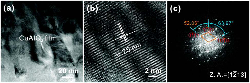 | ||
| Fig. 3 (a) HRTEM image of the CuAlO2 films grown at a substrate temperature of 940 °C (F3); (b) HRTEM image of the bulk of an individual grain and (c) its FFT pattern. | ||
The XPS Cu 2p, Al 2p, and O 1s core level spectra of sample F3 are shown in Fig. 4. The spectra were referred to the Au 4f7/2 core level (83.98 eV) of a freshly sputtered gold standard. The deconvolution of the Cu 2p peak [Fig. 4(a)] exhibited two peaks at ∼932.6 eV (Cu 2p3/2) and ∼952.4 eV (Cu 2p1/2), respectively, all attributed to Cu+1 in the CuAlO2 lattice. Traces of Cu0 and Cu+2 (the Cu 2p3/2 peak at ∼933.6 eV and the Cu 2p1/2 peak at ∼953.2 eV) were not observed, indicating that Cu+1 ions were completely oxidized and fully coordinated with O−2. Since the spin orbital-splitting of Cu 2p is ∼19.8 eV, the 2p3/2 and 2p1/2 peaks were not constrained for the area ratio during fitting. Nevertheless, the area ratio of the Cu 2p3/2 peak and the Cu 2p1/2 peak is ∼1.92 ± 0.08, being close to the ideal value of 2 determined from electron state densities. As a reference, the spectrum of the Cu 2p core level in +2 oxidation state, collected from the controlled samples prepared by atmospheric post-annealing, is also shown in the inset of Fig. 4(a). Two characteristic Cu+2 peaks, the 2p3/2 peak at ∼933.5 eV and the 2p1/2 peak at ∼953.6 eV, are evident. Moreover, a satellite (“shake-up”) peak at the binding energy of ∼938–946 eV is emerged as well. The appearance of the “shake-up” peak at around ∼943 eV is a fingerprint of the presence of Cu+2. The “shake-up” peak was reported for Cu+2, but it was absent in Cu+1 due to the multiplet splitting in the 2p53d9 final state.34 The Al 2p peak at ∼74.60 eV [Fig. 4(b)] is ascribed to Al+3–O−2 bonds, being shifted towards the higher binding energy with respect to the Al–Al chemical state (∼72.8 eV). The dominant peak at ∼531.30 eV in the O 1s peak shown in Fig. 4(c) should be assigned to O−2–Cu+1 (∼531.10 eV) and O−2–Al+3 (∼531.40 eV) bonds due to their small mutual chemical shift and inherently broad O 1s core level. It should be noted that, however, the peak at ∼532.3 eV, attributed to oxygen associated with OH− in hydroxide, can hardly be distinguished.11 It suggests the absence of OH-groups around the films surface exposure to air and this observation is well consistent with the FT-IR results. The FT-IR peak centered at ∼3368 cm−1, corresponding to the stretching vibration of the OH-group, was not observed in the case of all the four Cu–Al–O films in the wavenumber range of 4000–2400 cm−1 (not shown here), indicating the absence of OH-groups both inside the bulk films and surface.
 | ||
| Fig. 4 (a) Cu 2p, (b) Al 2p, (c) O 1s core level XPS spectra of the CuAlO2 films grown at a substrate temperature of 940 °C (F3). Inset in (a) shows the complete Cu+2 oxidation state dominated Cu 2p core level spectrum collected from the controlled samples prepared by atmospheric post-deposition annealing. (d) The crystal structure of delafossite CuAlO2. Red atoms are O, green Al, and orange Cu. | ||
UV-Vis absorption spectra were used to gain further insights into the optical properties of the films induced by the improvement of their crystallinity and phase-purity quantitatively and qualitatively. The UV-Vis absorption spectra were collected from the reflection mode using the 60 mm integrating sphere. 100 nm SiO2 coated n-Si wafers were used as reference samples. In such cases, the absorption from the reference bare substrates can be fully filtered. Fig. 5(a) shows the UV-Vis absorption spectra of samples F1–F4. The fundamental absorption edges for all samples were located in the ultraviolet regions (<380 nm) irrespective of the crystallinity and phase compositions, which are considered to be due to the band edge absorption of the samples. However, a blue-shift of the absorption edges was observed as the growth temperature increases, indicating that bandgaps of the Cu–Al–O films were enlarged with the improvement of their crystallinity and phase-purity. The direct optical bandgap, Eg, was estimated by extrapolating the linear portion of the (αhν)2vs. hν plot as shown in the inset of Fig. 5(a), where α is the absorption coefficient and hν is the incident photon energy. α was calculated based on the following equation:
 | (3) |
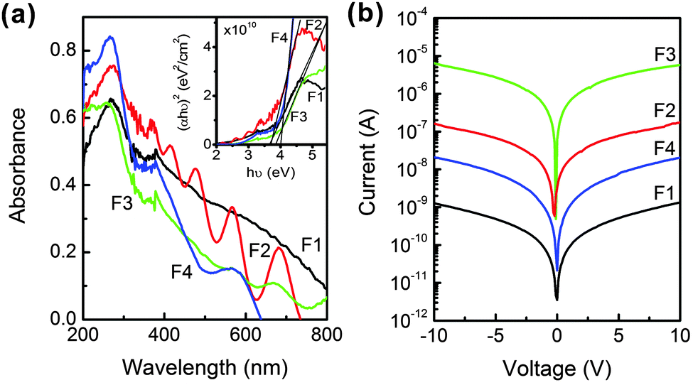 | ||
| Fig. 5 (a) UV-Vis absorption spectra and (b) I–V characteristics of the Cu–Al–O films (sample F1–F4). | ||
The electrical conductions of the Cu–Al–O films were first measured by I–V analyses using a two-probe method at room temperature in ambient air, as shown in Fig. 5(b). Al/Au contacts were deposited on the periphery of the films in the Van der Pauw configuration, and the linear I–V relationships confirm the Ohmic contact between Al/Au electrodes and films. The conduction was found to be increased by ∼4 orders of magnitude with the improvement of crystallinity and phase purity from samples F1–F3. However, the conduction of sample F4 dropped again due to the formation of impurity phases of CuAl2O4 and Al2O3 at high temperatures of over 1000 °C. It is noted that due to the poor conductive properties of samples F1 and F4, it is not reliable to evaluate the carrier concentrations and mobilities by employing Hall measurements. However, a uniform p-type conduction of these two samples was identically observed by the hot point probe test. Interestingly, uniform p-type conduction was also verified for samples F2 and F3 by using AC field Hall measurement method. The conductivities, hole concentrations, and Hall mobilities were revealed to be 1.47 × 10⁻³ (Ω cm)−1, 1.12 × 1016 cm3 and 0.82 cm2 V−1 s−1 (F2), and 9.8 × 10⁻² (Ω cm)−1, 7.12 × 1016 cm3 and 8.6 cm2 V−1 s−1 (F3), respectively. It should be noted here that the semiconductor properties in the case of the single-step deposited intrinsic r-CuAlO2 films are better than the films prepared by two steps with post-annealing.25 It is generally reported that defects play an important role in the p-type conductivity of Cu-based oxides. Acceptors (e.g. copper vacancies and interstitial oxygen) always have lower formation energies than donors (e.g. oxygen vacancies and interstitial copper).9,13–16,33 Based on the composition analysis of our films, copper vacancies and interstitial oxygen should be responsible for the enhanced hole-conductivity of p-CuAlO2 thin films. This is well consistent with previous reports.36,37
The observation of strong dependence of optical and electrical properties of r-CuAlO2 films on their crystallinity and phase composition demonstrates that the growth and semiconductor characteristics of delafossite CuAlO2 are more complicated than the conventional oxide semiconductors. From the thermodynamic standpoint, phase transitions between CuO–Cu2O–CuAlO2–CuAl2O4–Al2O3 are easily to occur, which leads to a narrow temperature window for growing phase-pure r-CuAlO2 films (∼940 °C), as demonstrated in this work. On the other hand, the highly directional O 2p-Cu 3d hybridized valence orbitals induce strong anisotropy of the high hole effective masses of ∼2 (δ = (m[100] + m[010])/2m[001] where 1.01 me[100], 0.38 me[010], 0.35 me[001]).3,38 Therefore their electronic structure and the hole transport properties are sensitive to the lattice distortions, which is considered to be a common and inherent feature of most of p-type WBOSs and other covalent semiconductors (such as Si) whose VBMs are composed of highly directional, anisotropic valence orbitals such as p, d or hybridized p–d or s–p.5,8 This shows sharp contrast to n-type WBOSs, in which the conduction band minimums (CBMs) are primarily contributed by spatially spread, isotropic s orbitals of cations (e.g. In2O3 81%, CdO 79%, α-Ga2O3 66%, and ZnO 45%).1 The charge transport properties of n-type WBOSs are thus insensitive to the presence of structural disorder and high electron mobilities are achievable even in amorphous structures.5 However, in view of the significant difference of the electronic configurations in CBMs and VBMs, reasonable electronic properties could hardly be achieved in poorly crystallized or amorphous p-type WBOSs with directional valence orbitals.
Conclusions
In summary, a single-step growth method for preparing r-CuAlO2 films by magnetron sputtering was reported. The crystallinity and phase composition of the Cu–Al–O films were revealed to be highly sensitive to the growth conditions, in particular the substrate temperature. The crystallite size increased with growth temperatures, and the highly crystallized rhombohedral CuAlO2 films were obtained in a narrow temperature window of ∼940 °C. The films deposited under optimal conditions were verified to have a columnar structure with a well-developed crystalline structure in column bulk. The films are transparent in the visible light region, and the high crystallinity of the films led to a band edge absorption at 3.86 eV. An increase of conductance by four orders of magnitude was also observed. The predominant role of crystallinity of r-CuAlO2 films in determining their electronic properties was demonstrated to be due to the heavy anisotropic characteristics of the O 2p-Cu 3d hybridized valence orbitals.Acknowledgements
This work was supported by the Natural Science Foundation of China (Grants No. 51202224, 91233101, 11174256, 51001091, U1304514, 21401167, 51402263), the Key Scientific Research Project of the Education Department of Henan Province (14A430031), State Key Basic Research Program, Ministry of Science and Technology of China (2014CB931704), and China Postdoctoral Science Foundation (2014M560602).Notes and references
- A. Facchetti and T. Marks, Transparent Electronics: From Synthesis to Applications, Wiley, 2010 Search PubMed.
- E. Fortunato and R. Martins, Phys. Status Solidi RRL, 2011, 5, 336 CrossRef CAS.
- G. Hautier, A. Miglio, G. Ceder, G.-M. Rignanese and X. Gonze, Nat. Commun., 2013, 4, 2292 CrossRef PubMed.
- M. S. Miao, S. Yarbro, P. T. Barton and R. Seshadri, Phys. Rev. B: Condens. Matter Mater. Phys., 2014, 89, 045306 CrossRef.
- K. Nomura, H. Ohta, A. Takagi, T. Kamiya, M. Hirano and H. Hosono, Nature, 2004, 435, 488 CrossRef PubMed.
- L. Wang, M. H. Yoon, G. Lu, Y. Yang, A. Facchetti and T. J. Marks, Nat. Mater., 2006, 5, 893 CrossRef CAS PubMed.
- K. K. Banger, Y. Yamashita, K. Mori, R. L. Peterson, T. Leedham, J. Rickard and H. Sirringhaus, Nat. Mater., 2011, 10, 45 CrossRef CAS PubMed.
- M. T. Greiner, M. G. Helander, W. M. Tang, Z. B. Wang, J. Qiu and Z. H. Lu, Nat. Mater., 2012, 11, 76 CrossRef CAS PubMed.
- J. Robertson and S. J. Clark, Phys. Rev. B: Condens. Matter Mater. Phys., 2011, 83, 075205 CrossRef.
- Z. Q. Yao, S. L. Liu, L. Zhang, B. He, A. Kumar, X. Jiang, W. J. Zhang and G. Shao, Appl. Phys. Lett., 2012, 101, 042114 CrossRef PubMed.
- P. K. Nayak, J. A. Caraveo-Frescas, Z. W. Wang, M. N. Hedhili, Q. X. Wang and H. N. Alshareef, Sci. Rep., 2014, 4, 4472 Search PubMed.
- A. Tsukazaki, A. Ohtomo, T. Onuma, M. Ohtani, T. Makino, M. Sumiya, K. Ohtani, S. F. Chichibu, S. Fuke, Y. Segawa, H. Ohno, H. Koinuma and M. Kawasaki, Nat. Mater., 2005, 4, 42 CrossRef CAS.
- D. O. Scanlon, K. G. Godinho, B. J. Morgan and G. W. Watson, J. Chem. Phys., 2010, 132, 024707 CrossRef PubMed.
- D. O. Scanlon and G. W. Watson, J. Phys. Chem. Lett., 2010, 1, 3195 CrossRef CAS.
- M. N. Huda, Y. F. Yan, A. Walsh, S. H. Wei and M. M. Al-Jassim, Phys. Rev. B: Condens. Matter Mater. Phys., 2009, 80, 035205 CrossRef.
- J. Vidal, F. Trani, F. Bruneval, M. A. L. Marques and S. Botti, Phys. Rev. Lett., 2010, 104, 136401 CrossRef.
- F. A. Benko and F. P. Koffyberg, J. Phys. Chem. Solids, 1984, 45, 57 CrossRef CAS.
- H. Kawazoe, M. Yasukawa, H. Hyodou, M. Kurita, H. Yanagi and H. Hosono, Nature, 1997, 389, 939 CrossRef CAS PubMed.
- M. Neumann-Spallart and R. Pinto, Thin Solid Films, 2011, 520, 1299 CrossRef CAS PubMed.
- B. Ling, J. L. Zhao, X. W. Sun, S. T. Tan, A. K. K. Kyaw, Y. Divayana and Z. L. Dong, Appl. Phys. Lett., 2010, 97, 013101 CrossRef PubMed.
- J. L. Cai and H. Gong, J. Appl. Phys., 2005, 98, 033707 CrossRef PubMed.
- M. Ohashi, Y. Iida and H. Morikawa, J. Am. Ceram. Soc., 2002, 85, 270 CrossRef CAS PubMed.
- S. Sato, M. Iijima, T. Nakayama, T. Sodesawa and F. Nozaki, J. Catal., 1997, 169, 447 CrossRef CAS.
- J. Tate, H. L. Ju, J. C. Moon, A. Zakutayev, A. P. Richard, J. Russell and D. H. McIntyre, Phys. Rev. B: Condens. Matter Mater. Phys., 2009, 80, 165206 CrossRef.
- R. S. Yu, S. C. Liang, C. J. Lu, D. C. Tasi and F. S. Shieu, Appl. Phys. Lett., 2007, 90, 191117 CrossRef PubMed.
- B. Ling, J. L. Zhao, X. W. Sun, S. T. Tan, A. K. K. Kyaw, Y. Divayana and Z. L. Dong, Appl. Phys. Lett., 2010, 97, 013101 CrossRef PubMed.
- B. L. Stevens, C. A. Hoel, C. Swanborg, Y. Tang, C. Zhou, M. Grayson, K. R. Poeppelmeier and S. A. Barnett, J. Vac. Sci. Technol., A, 2011, 29, 011018 Search PubMed.
- A. N. Banerjee, S. Kundoo and K. K. Chattopadhyay, Thin Solid Films, 2003, 440, 5 CrossRef CAS.
- P. H. Hsieh, Y. M. Lu, W. S. Hwang, W. L. Jang, C. L. Dong and T. S. Chan, Mater. Chem. Phys., 2014, 144, 547 CrossRef CAS PubMed.
- Y. S. Zou, H. P. Wang, S. L. Zhang, D. Lou, Y. H. Dong, X. F. Song and H. B. Zeng, RSC Adv., 2014, 4, 41294 RSC.
- Y. C. Zhang, J. Y. Tang, G. L. Wang, M. Zhang and X. Y. Hu, J. Cryst. Growth, 2006, 294, 278 CrossRef CAS PubMed.
- G. Kliche and Z. V. Popovic, Phys. Rev. B: Condens. Matter Mater. Phys., 1990, 42, 10060 CrossRef CAS.
- D. O. Scanlon, B. J. Morgan, G. W. Watson and A. Walsh, Phys. Rev. Lett., 2009, 103, 096405 CrossRef.
- J. Ghijsen, L. H. Tjeng, J. van Elp, H. Eskes, J. Westerink, G. A. Sawatzky and M. T. Czyzyk, Phys. Rev. B: Condens. Matter Mater. Phys., 1988, 38, 11322 CrossRef CAS.
- W. Walukiewicz, W. Shan, K. M. Yu, J. W. Ager III, E. E. Haller, I. Miotkowski, M. J. Seong, H. Alawadhi and A. K. Ramdas, Phys. Rev. Lett., 2000, 85, 1552 CrossRef CAS.
- B. J. Ingram, B. J. Harder, N. W. Hrabe and T. O. Mason, Chem. Mater., 2004, 16, 5623 CrossRef CAS.
- A. N. Banerjee, C. K. Ghosh and K. K. Chattopadhyay, Sol. Energy Mater. Sol. Cells, 2005, 89, 75 CrossRef CAS PubMed.
- L. J. Shi, Z. J. Fang and J. Li, J. Appl. Phys., 2008, 104, 073527 CrossRef PubMed.
| This journal is © the Owner Societies 2015 |