DOI:
10.1039/C4CC10209F
(Communication)
Chem. Commun., 2015,
51, 9173-9176
Highly reliable switching via phase transition using hydrogen peroxide in homogeneous and multi-layered GaZnOx-based resistive random access memory devices†
Received
21st December 2014
, Accepted 23rd April 2015
First published on 27th April 2015
Abstract
Here, we propose an effective method for improving the resistive switching characteristics of solution-processed gallium-doped zinc oxide (GaZnOx) resistive random access memory (RRAM) devices using hydrogen peroxide. Our results imply that solution processed GaZnOx RRAM devices could be one of the candidates for the development of low cost RRAM.
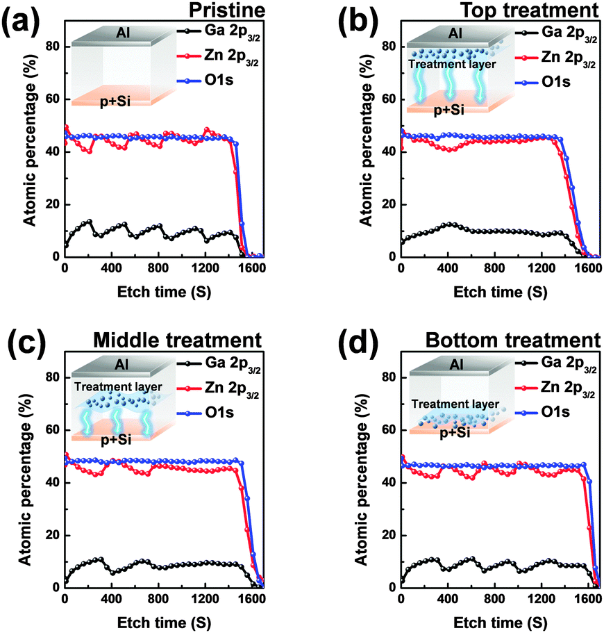
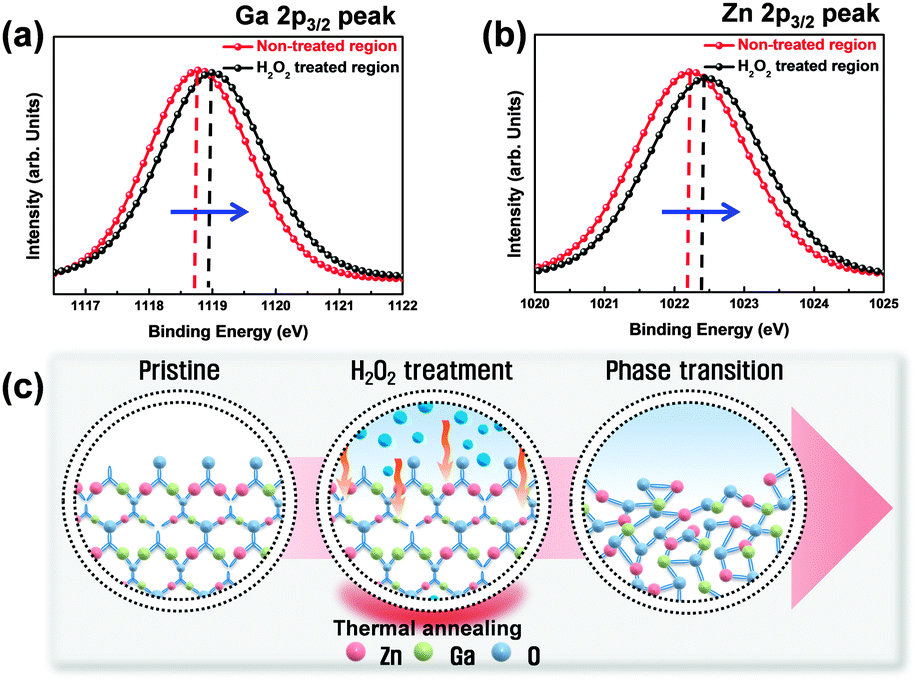
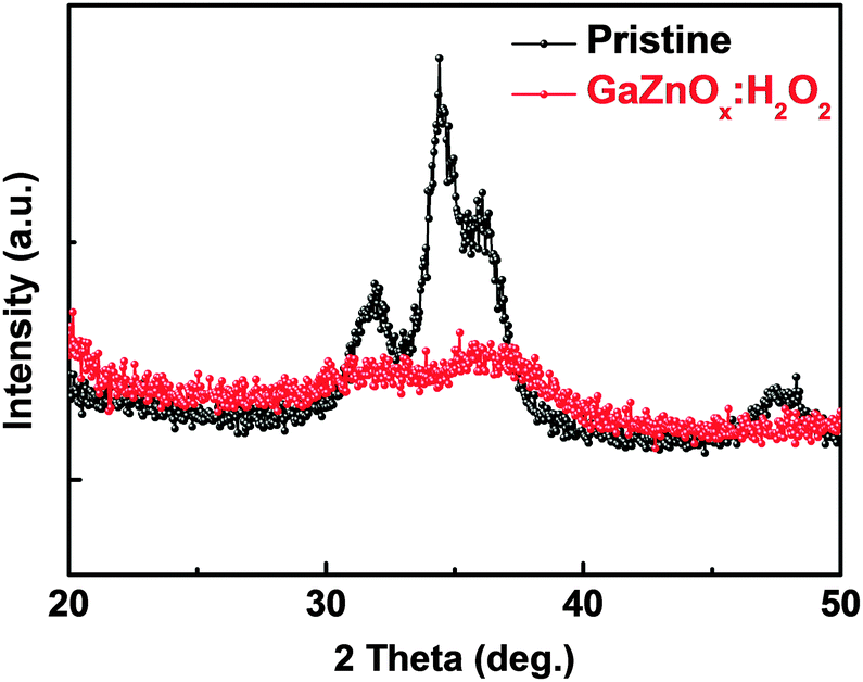
Conventional nonvolatile flash memory has been extensively studied in recent years due to its low fabrication cost and density comparable to that of 2X nm generations. However, flash memory still suffers from limitations such as low endurance, low write speed, and high voltage requirements for write operations.1 In addition, the downscaling of flash memory is expected to reach physical limits in near future due to retention degradation. When the tunnelling oxide thickness is less than 10 nm, stored charges of the floating gate easily escape because of defects in the tunnelling oxide, formed by repeated write/erase operations or direct tunnelling current.2 Hence, resistive random access memory (RRAM) based on reversible resistive switching (RS) behaviour has been extensively studied for use in next-generation nonvolatile data-storage devices.2–5 Many candidate materials have been reported for RRAM devices, including transition metal oxides (TMOs), perovskites such as Pr0.7Ca0.3MnO3 and SrZrO3, amorphous silicon, organic and inorganic materials.3–9 Among these materials, TMOs are promising candidates as they exhibit reliable and stable switching, improved high resistance state to low resistance state (HRS/LRS) ratios, high endurance, and complementary metal oxide semiconductor (CMOS) process compatibility.10,11 In particular, zinc oxide (ZnO) based TMOs have been actively investigated since they are considered to be environmentally friendly,12 exhibit a large HRS/LRS ratio, are transparent and flexible, and their raw materials are available in natural abundance.13,14 Gallium-doped zinc oxide (GaZnOx) has shown particular promise recently for its low cost and thermal stability.15 GaZnOx can be fabricated using various techniques including atomic layer deposition,16 pulse laser deposition,17 sputtering,18 and a solution process.19 The solution process has a number of advantages, including the simplicity of the process, easy control of substances, low cost, and selective deposition.20 Among the solution process technologies, however, the spin coating method requires repeated processing to achieve optimized active layer thickness, which may result in interface barriers between active layers that affect the RS characteristics of the RRAM device. Also, solution processed TMOs contain intrinsic oxygen vacancies, denoted VO, which may be shown through a filament model to form a conduction path in storage media.21 Among switching mechanism models, the widely used nanoscale conductive VO filament model shows applicability to an extensive range of materials and compares well to experimental measurements;21 use of this model has demonstrated that control of oxygen species (oxygen and VO) is necessary for improving RS characteristics. Also, reducing the number of VO filaments assists in lowering the RESET current and raising the resistance. Many studies have been undertaken to ameliorate these problems via doping, post-treatment, and development of multi-layer structures.2,22,23 In this communication, we propose an effective method for controlling VO concentrations, and investigate the phenomenon of phase transition using hydrogen peroxide (H2O2) in solution processed GaZnOx RRAM devices with a homogeneous multi-layered (HML) structure. Aluminum and heavily doped p-type silicon (p+Si) were used for the top and bottom electrodes, respectively; these are conventional materials in microelectronics systems, and serve as a good integration platform. Lastly, we studied the correlation between switching behavior and the material phase of GaZnOx by varying the deposition location of H2O2 treated GaZnOx: pristine, top (top treatment), middle (middle treatment), and bottom (bottom treatment). Detailed experimental conditions and steps are provided in the ESI.†Fig. 1 shows the atomic percentage with depth for each H2O2-treated GaZnOx thin film according to deposition location: pristine 1(a), top 1(b), middle 1(c), and bottom deposition 1(d), analyzed using X-ray photoelectron spectroscopy (XPS). XPS spectra were obtained using an Al monochromated X-ray source (Al Kα line: 1486.6 eV). The etch rate of the XPS depth analysis was 0.15 nm s−1 using ionic Ar at 1 keV. We observed that atomic percentages of Ga and Zn fluctuate periodically in the pristine GaZnOx film with increasing etch time, as shown in Fig. 1(a). These results suggest that the Ga and Zn composition in the multi-layered pristine GaZnOx thin film is segregated at the interfaces during the pre-annealing process, since the film was formed using five repeated processes to optimize the thickness (four times for each pristine GaZnOx sub-layer and once for H2O2-embedded GaZnOx). This segregation may derive from doping inefficiencies or from the maximum solubility of Ga.24 The segregated phase at the interface can affect the formation and rupture of VO filaments, which degrades the electrical characteristics of a RRAM device. The top-treated GaZnOx thin film, however, showed smooth atomic Ga and Zn percentages, as shown in Fig. 1(b). These results indicate the effect of H2O2 on HML GaZnOx thin films. XPS depth profiles were also measured for the other deposition locations (middle and bottom). Fig. 1(c) and (d) clearly shows smooth Ga and Zn atomic percentages, blended by the H2O2 treatment. This implies that atomic arrangement varies for GaZnOx treated with H2O2 when compared with the pristine GaZnOx thin film. Fig. 2(a) and (b) show the XPS depth spectra for Ga 2p3/2 and Zn 2p3/2 peaks, for both H2O2-treated GaZnOx and the non-treated GaZnOx region in the middle-treated GaZnOx thin film. Each spectrum was deconvoluted using a Gaussian distribution after correcting for background. The Ga 2p3/2 and Zn 2p3/2 spectra were centered at 1118.77 eV and 1022.21 eV, respectively, corresponding to GaO and ZnO.25,26 As shown in Fig. 2(a) and (b), the Ga 2p3/2 and Zn 2p3/2 peaks shift to higher binding energy in the H2O2-treated GaZnOx region, suggesting that the GaO–ZnO film formed not just as a physical mixture with two distinct GaO and ZnO phases, but that an enhanced oxidation state was found in the GaZnOx system. Based on the above results, the effects of H2O2 treatment on the GaZnOx film can be clearly seen. Oxygen radical diffusion by H2O2 dissociation may affect the GaZnOx phase during pre-annealing. These results are consistent with the study by Tsai et al.,27 who assumed that the phase of the ZnO film can be changed from polycrystalline to amorphous-like by penetration of dissociated oxygen radicals. Fig. 2(c) shows the phase transition and blended arrangement of Ga and Zn due to H2O2 treatment schematically, after 300 °C pre-annealing. To verify the phase transition and crystallinity of H2O2-treated GaZnOx films by oxygen radical diffusion, we compared the H2O2-treated GaZnOx film with the pristine GaZnOx film using grazing incidence X-ray diffraction (GIXRD), with a 3 kW sealed X-ray tube Cu Kα (λ = 1.541 Å), as shown in Fig. 3. For the pristine GaZnOx film, XRD analysis revealed no diffraction peaks, implying the amorphous phase. However, the H2O2-treated GaZnOx film was found to be in the c-axis oriented polycrystalline phase, with the highest peak observed at 34.48°,28 indicating a GaZnOx phase transition instigated by H2O2 treatment. Overall, the H2O2-induced phase transition correlates well with the results of the previous study in terms of oxygen radical diffusion.27 We analyzed the electrical characteristics of all devices to investigate the effect of H2O2 treatment on HML GaZnOx RRAM devices. Fig. 4 shows the current–voltage (I–V) characteristics of the devices according
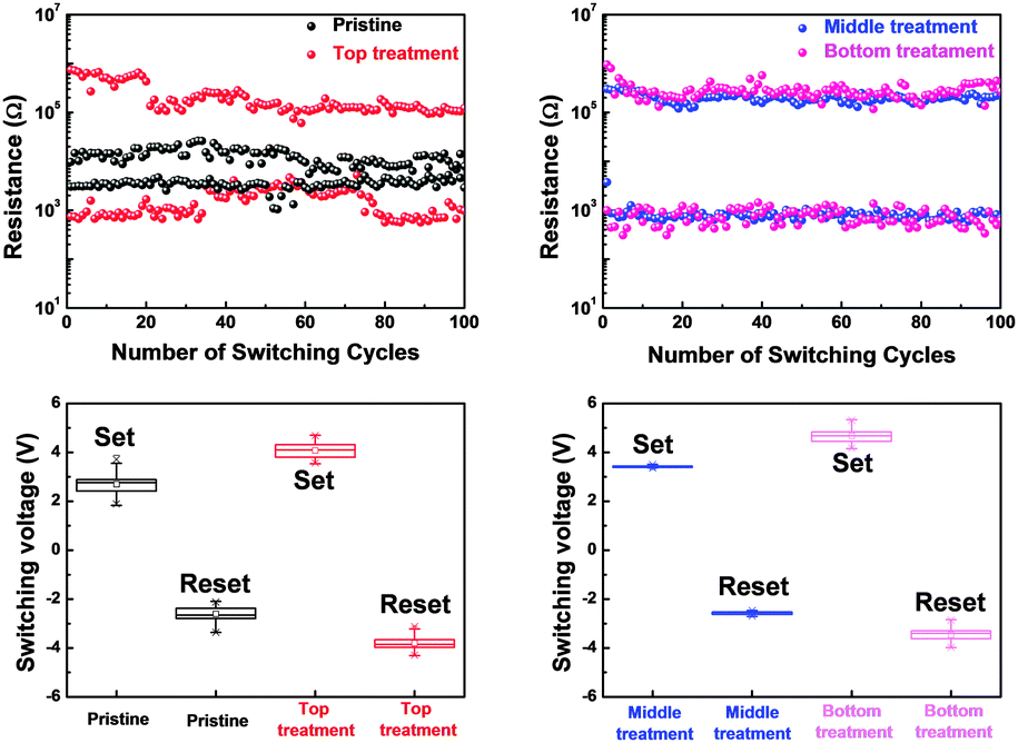
to the deposition location. All devices show clear BRS characteristics. This bi-stable switching is due to the formation and rupture of VO filaments.21 The bottom electrode was ground, and a bias voltage (positive and negative) was applied to the top electrode for switching the device. When a sweep voltage ranging from zero to positive was applied to the top electrode of the pristine GaZnOx device, a sudden decrease in resistance from HRS to LRS (defined as the SET process) was observed at about +2.43 V. As the applied voltage swept from positive to zero, LRS was maintained. Sweeping from zero to negative, an increase in resistance from LRS to HRS (defined as the RESET process) was observed at about −2.19 V. As the applied voltage swept from negative to zero, HRS was maintained. The current was limited to 7 mA during the high-to-low and low-to-high resistance switching processes to avoid permanent damage to the devices. The pristine GaZnOx-based device exhibited poor BRS characteristics as shown in Fig. 4(a). There are two possible explanations; the first is the generation of excess intrinsic VO in the solution processed GaZnOx thin film. Since the formation and rupture of conduction filaments (CFs) are attributed to VO, appropriate control of VO in TMO-based RRAM is a necessity. Therefore, excess intrinsic VO induces poor switching characteristics. The second explanation is that nanocrystalline grain boundaries in pristine GaZnOx cause non-uniform switching characteristics. Grain boundaries are known to be preferential sites for VO filament formation, it is therefore commonly accepted that excess electrical conduction paths might form due to the high number of grain boundaries in the nanocrystalline GaZnOx thin film.29 Also, random nucleation and growth of CFs along grain boundaries make their formation difficult to control, which is a significant impediment to device performance improvement. In contrast, top-, middle-, and bottom-treated GaZnOx devices exhibited an improvement in the switching window (of the order of ∼102) as shown in Fig. 4(b)–(d), respectively. For bottom-treated GaZnOx devices, however, HRS and LRS were shifted toward the low current level and showed a multi-step SET voltage (Fig. 4(d)). This phenomenon is attributed to the GaZnOx/Si interface at the bottom electrode, where a native oxide forms because of the strong oxidation potential of H2O2 and large free energy of formation.30–32 The formation of native oxide at the GaZnOx/Si interface interrupts the generation of uniform CFs and impedes current flow. To compare the electrical stability of devices, we carried out endurance tests at a reading voltage of 0.4 V and plotted SET/RESET distribution during 100 switching cycles, as shown in Fig. 5. With the exception of the pristine device, all devices showed enhanced endurance characteristics up to 100 cycles. However, resistance fluctuations were observed in top and bottom treated GaZnOx devices, possibly due to the amorphized GaZnOx phase transition and formation of native oxide at the bottom electrode. Also, the SET and RESET voltages for the top-treated GaZnOx device were higher than for the middle-treated sample, since H2O2 treatment increases the metal-oxide bond in GaZnOx and causes a material phase change from polycrystalline to amorphous. These results are consistent with middle-treated samples. In contrast, the middle-treated device exhibited a highly uniform SET/RESET distribution compared with other devices. Overall, the middle-treated GaZnOx device showed better BRS characteristics, including SET/RESET distribution, endurance, and switching window, amongst the four comparison groups. Fig. 6 shows a feasible BRS conduction mechanism for the middle-treated GaZnOx device. The schematic is based on characteristics resulting from the rupture and formation of conductive VO filaments at the interfaces between non-treated GaZnOx and H2O2-treated GaZnOx, caused by a redox reaction. When the applied voltage reaches the positive forming voltage to create a conduction path, oxygen ions attracted from the amorphous region move toward the top Al electrode and the VO simultaneously move downward. Compared with the non-treated GaZnOx layer, higher densities of lattice and interstitial oxygen ions exist in H2O2-treated GaZnOx, hence uniform CFs were formed in the H2O2-treated region. Thus, asymmetrically shaped CFs with weak CF offshoots were formed at the interface, causing the device to switch to the LRS. When a negative bias is applied to the top Al electrode, the repelled oxygen ions from the non-treated polycrystalline region move to the polycrystalline/amorphous interface, where they induce local Joule heating and oxidation. The narrow size of the asymmetric CFs at the interface induces intense local Joule heating, resulting in switching to HRS. This localized interface RS reduces the problem of escape of oxygen ions from electrodes in the middle-treated device.33 Hence, the middle-treated device showed superb RS characteristics compared with other devices, with improved switching parameters such as SET/RESET distribution, endurance and on/off ratio.
 |
| | Fig. 1 XPS depth profiles to observe composition variations according to deposition location of H2O2-treated GaZnOx thin films for (a) pristine, (b) top treatment, (c) middle treatment, and (d) bottom treatment (the inset image shows the schematic of the deposition location of the H2O2-treated GaZnOx thin film). | |
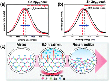 |
| | Fig. 2 XPS results for (a) Ga 2p3/2 and (b) Zn 2p3/2 peaks for middle-treated GaZnOx thin film (c) schematic of phase transition. | |
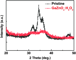 |
| | Fig. 3 Grazing incidence X-ray diffraction patterns of GaZnOx thin films with and without H2O2. | |
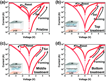 |
| | Fig. 4
I–V characteristics of the HML structure RRAM devices for (a) pristine, (b) top treatment, (c) middle treatment, and (d) bottom treatment. | |
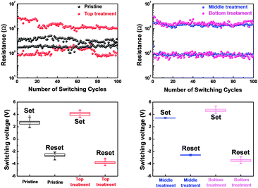 |
| | Fig. 5 Comparison of endurance characteristics and SET/RESET voltage distribution of the HML structure RRAM devices. | |
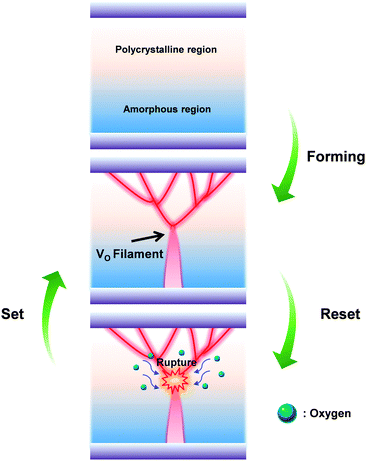 |
| | Fig. 6 The conduction mechanism schematic for the BRS in the middle-treated GaZnOx RRAM device. | |
In this communication, we investigated the phase transition of solution-based HML GaZnOx RRAM devices using H2O2 to improve the RS characteristics such as SET/RESET uniformity, endurance, and switching window. Significant variations in I–V characteristics were observed, depending on the deposition location of H2O2-treated GaZnOx. The pristine GaZnOx based device exhibited poor BRS characteristics such as large variation in switching voltage, narrow switching window, and poor reproducibility during repeated switching cycles. In contrast, the H2O2-treated RRAM devices showed improved BRS characteristics. In particular, the middle-treated device exhibited a high LRS/HRS ratio (of the order of ∼102), stable endurance, and narrow dispersion of SET/RESET switching voltage. These results suggest that H2O2-treated GaZnOx solution both assisted physical mixing in the segregated material system, and changed the material phase from polycrystalline to amorphous in pristine GaZnOx layers. Furthermore, H2O2 effectively smoothens interfaces via diffusion of oxygen radicals dissociated from H2O2 in solution-based HML GaZnOx RRAM devices. Solution based HML GaZnOx RRAM devices using H2O2 therefore enable the realization of low-cost portable electronics.
This work was supported by the National Research Foundation of Korea (NRF) grant funded by the Korea government (MSIP) [No. 2011-0028819].
Notes and references
- S. Tehrani, J. M. Slaughter, E. Chen, M. Durlam, J. Shi and M. DeHerrera, IEEE Trans. Magn., 1999, 35, 2814 CrossRef.
- D. H. Yoon, S. J. Kim, J. Jung, H. S. Lim and H. J. Kim, J. Mater. Chem., 2012, 22, 17568 RSC.
- B. Sun, W. Zhao, L. Wei, H. Li and P. Chen, Chem. Commun., 2014, 50, 13142 RSC.
- M. J. Rozenberg, I. H. Inoue and M. J. Sánchez, Phys. Rev. Lett., 2004, 92, 178302 CrossRef CAS.
- M. C. Wu, W. Y. Jang, C. H. Lin and T. Y. Tseng, Semicond. Sci. Technol., 2012, 27, 065010 CrossRef.
- B. M. Köpe, M. Tendulkar, S. G. Park, H. D. Lee and Y. Nishi, Nanotechnology, 2011, 22, 254029 CrossRef PubMed.
- S. H. Jo, K.-H. Kim and W. Lu, Nano Lett., 2008, 9, 496 CrossRef PubMed.
- C.-J. Jung, J.-H. Wu and G.-S. Liou, Chem. Commun., 2014, 50, 4335 RSC.
- F. Pan, S. Gao, C. Chen, C. Song and F. Zeng, Mater. Sci. Eng., R, 2014, 83, 1–59 CrossRef PubMed.
- W. Y. Chang, Y. C. Lai, T. B. Wu, S. F. Wang, F. Chen and M. J. Tsai, Appl. Phys. Lett., 2008, 92, 022110 CrossRef PubMed.
- H. Lv, X. Xu, H. Liu, R. Liu, Q. Liu, W. Banerjee, H. Sun, S. Long, L. Li and M. Liu, Sci. Rep., 2015, 5, 7764 CrossRef PubMed.
- F. Tamaddon, M. A. Amrollahi and L. Sharafat, Tetrahedron Lett., 2005, 46, 7841 CrossRef CAS PubMed.
- Y. C. Yang, F. Pan, Q. Liu, M. Liu and F. Zeng, Nano Lett., 2009, 9, 1636 CrossRef CAS PubMed.
- Z. Q. Wang, H. Y. Xu, X. H. Li, X. T. Zhang, Y. X. Liu and Y. C. Liu, IEEE Electron Device Lett., 2011, 32, 1442 CrossRef CAS.
- B. D. Ahn, S. H. Oh, H. J. Kim, M. H. Jung and Y. G. Ko, Appl. Phys. Lett., 2007, 91, 252109 CrossRef PubMed.
- S. J. Lim, S. J. Kwon, H. Kim and J. S. Park, Appl. Phys. Lett., 2007, 91, 183517 CrossRef PubMed.
- H. Frenzel, A. Lajn, M. Brandt, H. von Wenckstern, G. Biehne, H. Hochmuth, M. Lorenz and M. Grundmann, Appl. Phys. Lett., 2008, 92, 192108 CrossRef PubMed.
- Y. J. Tak, D. H. Yoon, S. Yoon, U. H. Choi, M. M. Sabri, B. D. Ahn and H. J. Kim, ACS Appl. Mater. Interfaces, 2014, 6, 6399 CAS.
- C. H. Kim, Y. S. Rim and H. J. Kim, ACS Appl. Mater. Interfaces, 2013, 5, 6108 CAS.
- S. J. Heo, D. H. Yoon, T. S. Jung and H. J. Kim, J. Inf. Disp., 2013, 14, 79 CrossRef CAS PubMed.
- N. Xu, L. Liu, X. Sun, X. Liu, D. Han, Y. Wang, R. Han, J. Kang and B. Yu, Appl. Phys. Lett., 2008, 92, 232112 CrossRef PubMed.
- D. H. Yoon, Y. J. Tak, S. P. Park, J. Jung, H. Lee and H. J. Kim, J. Mater. Chem. C, 2014, 2, 6148 RSC.
- Y. Bai, H. Wu, Y. Zhang, M. Wu, J. Zhang, N. Deng, H. Qian and J. Yu, Appl. Phys. Lett., 2013, 102, 173503 CrossRef PubMed.
- J. A. Sans, G. M. Criado, J. P. Porres, J. F. S. Royo and A. Segura, Appl. Phys. Lett., 2007, 91, 221904 CrossRef PubMed.
- T. Das, C. Mahata, C. K. Maiti, E. Miranda, G. Sutradhar and P. K. Bose, Appl. Phys. Lett., 2011, 98, 022901 CrossRef PubMed.
- J. L. Lan, S. J. Cherng, Y. H. Yang, Q. Zhang, S. Subramaniyan, F. S. Ohuchi, S. A. Jenekhe and G. Cao, J. Mater. Chem. A, 2014, 2, 9361 CAS.
- C. H. Tsai, W. C. Wang, F. L. Jenq, C. C. Liu, C. I. Hung and M. P. Houng, J. Appl. Phys., 2008, 104, 053521 CrossRef PubMed.
- W. J. Park, H. S. Shin, B. D. Ahn, G. H. Kim, S. M. Lee, K. H. Kim and H. J. Kim, Appl. Phys. Lett., 2008, 93, 083508 CrossRef PubMed.
- M. Lanza, K. Zhang, M. Porti, M. Nafría, Z. Y. Shen, L. F. Liu, J. F. Kang, D. Gilmer and G. Bersuker, Appl. Phys. Lett., 2012, 100, 123508 CrossRef PubMed.
- J. M. Kwon, J. Jung, Y. S. Rim, D. L. Kim and H. J. Kim, ACS Appl. Mater. Interfaces, 2014, 6, 3371 CAS.
- R. Waser, R. Dittmann, G. Staikov and K. Szot, Adv. Mater., 2009, 21, 2632 CrossRef CAS PubMed.
- Y. T. Chen, T. C. Chang, H. K. Peng, H. C. Tseng, J. J. Huang, J. B. Yang, A. K. Chu, T. F. Young and S. M. Sze, Appl. Phys. Lett., 2013, 102, 252902 CrossRef PubMed.
- D. Acharyya, A. Hazra and P. Bhattacharyya, Microelectron. Reliab., 2014, 54, 541 CrossRef CAS PubMed.
Footnote |
| † Electronic supplementary information (ESI) available. See DOI: 10.1039/c4cc10209f |
|
| This journal is © The Royal Society of Chemistry 2015 |
Click here to see how this site uses Cookies. View our privacy policy here. 
 Open Access Article
 This Open Access Article is licensed under a Creative Commons Attribution-Non Commercial 3.0 Unported Licence