SnO2 nanowire anchored graphene nanosheet matrix for the superior performance of Li-ion thin film battery anode†
Rajesh
Thomas
and
G.
Mohan Rao
*
Indian Institute of Science, Dept. of Instrumentation and Applied Physics, Malleshwaram PO IISc Bangalore, Bangalore, Karnataka 560012, India. E-mail: thomasphy@gmail.com
First published on 21st October 2014
Abstract
All solid state batteries are essential candidate for miniaturizing the portable electronics devices. Thin film batteries are constructed by layer by layer deposition of electrode materials by physical vapour deposition method. We propose a promising novel method and unique architecture, in which highly porous graphene sheet embedded with SnO2 nanowire could be employed as the anode electrode in lithium ion thin film battery. The vertically standing graphene flakes were synthesized by microwave plasma CVD and SnO2 nanowires based on a vapour–liquid–solid (VLS) mechanism via thermal evaporation at low synthesis temperature (620 °C). The graphene sheet/SnO2 nanowire composite electrode demonstrated stable cycling behaviours and delivered a initial high specific discharge capacity of 1335 mAh g−1 and 900 mAh g−1 after the 50th cycle. Furthermore, the SnO2 nanowire electrode displayed superior rate capabilities with various current densities.
1. Introduction
Lithium ion batteries (LIBs) are crucial systems for energy storage in electronic devices such as communication/portable devices, electric/hybrid vehicles and other power gadgets etc. LIBs offer many advantages, compared to other battery systems, like high energy density and high voltage, high charge capacity and stability, large cyclability and rate capability.1,2 The electrode materials play an important role in the performance of lithium batteries. Many advances have to be made to meet today's increasing demands in high energy density and high cycle rate by designing new nanomaterials and processing techniques. Current commercial Li ion batteries largely depend on graphite as the anode. It can be reversibly charged and discharged under intercalation potentials with reasonable specific capacity, but the low theoretical capacity (372 mAh g−1) of graphite prevents the use of LIBs for high energy and high power applications.3The developments of all solid state thin film batteries (TFB) are essential for the miniaturization of portable electronic devices and to avoid the problems caused by the liquid electrolyte. A thin film battery is composed of several electrochemical cells that are connected in series and/or in parallel to provide the required voltage and capacity. The solid state (micro batteries) is essential for state of the art microelectronic and portable electronic devices. The energy and power requirements for these devices are ever increased and lead to the research for novel battery structure and electrode materials with increased volume energy and power density.4,5 Due to their thinner dimension, TFBs have greater applications in making thinner electronic devices, RFID tags, wireless sensors and implantable medical devices.6,7 These batteries exhibit the same voltage and current as their bulky counterparts. The advancement of nanotechnology and cell engineering caused TFBs to achieve high energy density and cycle life.
Thin film batteries are built layer by layer by vapour deposition. There are various methods being used to deposit thin film electrode materials onto the current collector such as, sputtering, CVD and sol gel methods.8 Plasma based material deposition techniques are well suited for industrial applications. Multiple thin film cells can reduce the footprint of a large planar battery area; this will be a solution to attain large energy and power requirements. The first solid state thin film battery was developed by Hitachi Co., Japan in 1982.9 A thin film battery, with more stable LIPON as the solid electrolyte, was developed by a group at Oak ridge national laboratory.10 There are several companies and research institutions actively involved to develop better thin film battery systems.8 J. H. Pikul et al.11 have demonstrated that 3-D micro batteries from bicontinuous nanoporous electrodes gave the power density of 7.4 mW cm−2 μm−1. Graphene (having a high theoretical specific surface area of 2630 m2 g−1) or carbon nanostructures can enhance the storage capacity by several orders.12 Graphene can accommodate Li ions on both sides. This makes its theoretical capacity two times larger than (∼740 mAh g−1) that of other carbon materials.
In order to increase the battery's capability, various elements or compounds (e.g. Si, Sn, Ge, SnO2etc) are alloyed with lithium to get larger specific capacities than commercial graphite. Among the various metal and metal oxide based electrodes, both tin (Sn) and tin oxide (SnO2)13,14 have been discussed as important anode materials for Li-ion batteries, because of their semiconducting properties combined with high capacity (Sn, 994 mAh g−1 and SnO2 781 mAh g−1) higher than that of graphite.15 However, significant capacity fading with cycling is a problem specifically with metal oxide based materials due to large volume changes during Li alloying and dealloying, which leads to metal segregation, crystallographic deformation16 and agglomeration of active materials. In the case of Sn, the volume changes are as high as 259%.17
The huge volume changes associated with lithiation/delithiation process are a major drawback for SnO2 based electrodes, hindering it from real applications.18 In order to solve the issues associated with metal oxide materials, various nanostructured SnO2 and SnO2 composites have been proposed. These can be accommodating for volume changes during the cyclic process. Nanostructured electrode materials possess many advantages, such as increased number of electrochemical active sites and better control over stress due to the lithiation/delithiation process.19,20 Nanostructured metal oxide particles with homogeneous carbon coating have already been reported to improve the mechanical and electrochemical stability.21 The carbon support on nanoparticles enables a better accommodation of the large volume change and improves the electron conductivity of the electrode.22 Nanocarbon materials often gave high coulombic efficiencies and cycle life, but the volumetric energy density and rate performance were poor due to the formation of a large SEI film.23 By using nanostructured inorganic materials, the rates of the electron and counter ion transport are increased. Transport properties have been improved somewhat by using nano-architectured electrodes with large surface areas.24
Nanowires and nanoparticles of alloy materials are a better choice for advanced Li batteries. The transport of Li ions is one of the main issues that give rise to current limitations. Engineering the active materials into exceptional nano-architectures will enhance the efficiency of the electrochemical performance such as specific capacity, rate capabilities and cycling stability.25 Several studies have shown that SnO2 nanowire/heterostructures gave a capacity of ∼700 mAh g−1 up to 15 cycles26 then faded to ∼300 mAh g−1 after 50 cycles. Kim et al. have demonstrated stable cycling behaviour for SnO2 nanowire electrode which delivered a high specific discharge capacity of 510 mAh g−1.27 Graphene nanosheet (GNS) matrix having a flexible two-dimensional structure, high surface area (over 2600 m2 g−1), excellent electrical conductivity and the ability to diminish the stress of the electrode upon cycling will support SnO2 based nanostructures.28,29
In the present study, we are aiming for a higher electrochemical performance of the SnO2NW@GNS anode by adding the advantage of both materials vs. graphene nanosheets and SnO2 nanowires. We have modified the carbon into a graphene nanosheet (GNS) matrix and nanowires of SnO2 were embedded in it (SnO2NW@GNS). GNS consists of a few layers of graphene grown vertically over the substrate and provides very high porosity. The high surface area of GNS is able to attach more SnO2 nanowires on to the wall of the graphene sheet, thus easing the Li ion migration into the active materials. Hence, tailoring the structure of SnO2 materials or embedding them on carbon matrices should enhance the SnO2NW@GNS anode performance. It is well known that the following equations are involved in the SnO2 based anodes.
| SnO2 + 4Li+ + 4e− ↔ Sn + 2Li2O | (1) |
| Sn + xLi+ + xe− ↔ LixSn (0 ≤ x ≤ 4.4) | (2) |
The first reaction is considered irreversible and is responsible for the irreversible capacity loss from the first to the second discharge cycles.30,31 However, this irreversible capacity could also become reversible for nanometer-sized SnO2 nanoparticles or nanowires.32 The second equation is widely known for the reversible capacity, in which Li is continuously alloying with Sn.33 These kinds of nano-architectures of carbon are very suitable for energy storage applications.
2. Experimental
2.1. Synthesis of graphene nanosheet and SnO2 nanowire
The graphene nanosheet (GNS) was synthesized on a copper substrate using plasma enhanced (electron cyclotron resonance) ECR-CVD. In this method, acetylene (C2H2) was decomposed to graphene nanosheets in the presence of microwave plasma. The details of the GNS synthesis have been given in our previous report.34 For the growth of SnO2 nanowires, a thin layer of about 3 nm of gold has been sputtered over the GNS sample as the catalyst. Then the gold-coated GNS sample was annealed at 600 °C for 10 minutes. Gold particles of approximately 5 nm in size were formed over GNS after annealing. These spherical particles serve as catalysts for growing individual SnO2 nanowires. On these samples, SnO2 was deposited by reactive electron beam evaporation of Sn in the presence of oxygen. Prior to the evaporation of Sn, the substrate temperature was kept at 620 °C and the deposition rate of Sn was about 1.4 Å s−1. The oxygen partial pressure was maintained at 4 × 10⁻⁴ mbar and the deposition was carried out for 15 minutes. The nanowire growth took place at a very low evaporation rate of Sn. The total active material deposited over a 1.13 cm2 area of copper substrate weighed about 0.1 mg (including the weight of GNS and SnO2 nanowires). The mass of SnO2 deposited (about 100 nm thickness) determined using density calculation was about 7.85 × 10⁻⁵ g, as opposed to the mass of GNS which was about 2.15 × 10⁻⁵ g.2.2. Characterization of SnO2NW@GNS films
The surface morphologies of GNS and nanowires were characterized by field emission scanning electron microscopy (FESEM, ULTRA 55, Karl Zeiss). The X-ray diffraction (XRD, Rigaku Smartlab) pattern of the nanowire@GNS sample was obtained with a Cu Kα radiation source. The surface chemistry and bonding nature of the sample was analyzed with X-ray photoelectron spectroscopy (XPS, SPECS GmbH, Phoibos 100 MCD Energy Analyzer using Mg-Kα radiation, 1283.6 eV) and Raman spectrometer (LabRAM HR spectrometer with an Ar-ion laser at the wavelength of 514 nm, at a magnification of 100× and a CCD camera detector). The high resolution TEM (HRTEM, FEI TECNAI T20 microscope operated at 200 kV) was performed for the pristine sample and after electrochemical performance.2.3. Electrochemical measurements
The electrochemical testing was done in Swagelok cells with 1 M LiPF4 I EC/DMC (1![[thin space (1/6-em)]](https://www.rsc.org/images/entities/char_2009.gif) :
:![[thin space (1/6-em)]](https://www.rsc.org/images/entities/char_2009.gif) 1 w/w) as the electrolyte (EC = ethylene carbonate, DMC = dimethyl carbonate) and Li foil as the counter and reference electrode. The SnO2NW@GNS over the copper substrate was used as the anode electrode. Cells were assembled as half cell configuration in Ar-filled MBraun glove box model Unilab to avoid contamination and oxidation. The total weight of the active material was accurately measured by subtracting the mass of the sample before and after the deposition using a microbalance. We calculated the total capacity from the weight of the composite. Cells were galvanostatically charged and discharged at various current densities using a CHI 665 electrochemical workstation within the potential range of 2–0.1 V (vs. Li/Li+) at ambient temperature. Cyclic voltammetry (CV) was performed between 2.0 and 0.1 V at a scan rate of 0.5 mV s−1. Various current densities were used to study the rate capacity of the SnO2NW@GNS electrode.
1 w/w) as the electrolyte (EC = ethylene carbonate, DMC = dimethyl carbonate) and Li foil as the counter and reference electrode. The SnO2NW@GNS over the copper substrate was used as the anode electrode. Cells were assembled as half cell configuration in Ar-filled MBraun glove box model Unilab to avoid contamination and oxidation. The total weight of the active material was accurately measured by subtracting the mass of the sample before and after the deposition using a microbalance. We calculated the total capacity from the weight of the composite. Cells were galvanostatically charged and discharged at various current densities using a CHI 665 electrochemical workstation within the potential range of 2–0.1 V (vs. Li/Li+) at ambient temperature. Cyclic voltammetry (CV) was performed between 2.0 and 0.1 V at a scan rate of 0.5 mV s−1. Various current densities were used to study the rate capacity of the SnO2NW@GNS electrode.
3. Results and discussion
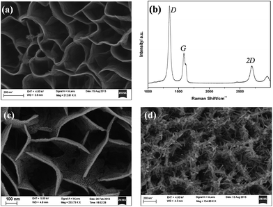
The morphology of the highly porous, vertically oriented graphene nanosheet film grown over a copper substrate is shown in Fig. 1a. Each wall of graphene sheet is a combination of several single graphene sheets. This porous structure of GNS gives a high surface to volume ratio and is very suitable for maximum Li storage. Li ions can attach to both sides of the graphene wall. Fig. 1b gives the Raman spectrum of the GNS thin film. The 2d peak at 2700 cm−1 shows the presence of many graphene layers. The very thin film of gold coated over the GNS sample is shown in Fig. 1c. After annealing at 600 °C, the spherical particles of gold were attached to the wall of GNS and these gold particles acted as sites for SnO2 nanowire growth. Fig. 1d shows the SnO2 nanowires on GNS (SnO2NW@GNS) after the initial growth stage (after 10 minutes of deposition) and it can be seen that the wires were attached to the graphene wall.Fig. 2a shows a typical field emission scanning electron microscopy (FESEM) image of the as-synthesized SnO2 nanowire grown over the GNS matrix with Au catalyst at a substrate temperature of 620 °C. The total time taken for the deposition of SnO2 nanowires was about 30 minutes. The long nanowires of SnO2 are seen in the porous structure of the GNS matrix. The wires are uniformly distributed over the GNS matrix. A cross section SEM image of SnO2NW@GNS is shown in Fig. 2b. All the nanowires are seen with a tip on the top (white circles on the cross section image) and were assumed to be an eutectic metal alloy, indicating that the nanowires were grown via tip-led growth according to the VLS mechanism.35
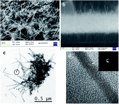 | ||
| Fig. 2 (a) FESEM image of SnO2 nanowires (b) cross section SEM image of SnO2 nanowires on GNS, (c) TEM image of SnO2NW@GNS nanowires and (d) HRTEM of single nanowire (inset) SAED pattern. | ||
The XRD pattern of the SnO2NW@GNS electrode is shown in the ESI (Fig. S1†). The peaks marked in the spectra are well matched with the rutile-tetragonal SnO2 phase (space group P42/mnm). A broad peak at 2θ = 21° was assigned to the graphitic peak coming from the GNS matrix.
Fig. 2c shows the transmission electron microscopy image of SnO2NW@GNS. The wires seem to arise from the graphene sheet (darker side of the image) with a eutectic metal alloy at the tip of each wire. An energy-dispersive (EDS) line scan of an individual nanowire from the tip along the nanowire stem indicated that the tip of the metal alloy was abundant of catalyst, gold, whereas the nanowire stem consisted of pure SnO2 without any presence of Au on it (ESI Fig. S2†). The HRTEM of a single nanowire of SnO2 confirmed that the as-synthesized wires are highly-ordered consisting of a single crystal phase with sharp periodic lattice fringe. Each nanowire is very thin with a diameter of ∼10 to 5 nm. The SAED pattern (inset of Fig. 2d) shows that the nanowires have the preferential growth direction of [101]. The inter-atomic plane distance calculated to the (101) lattice was 2.56 Å.
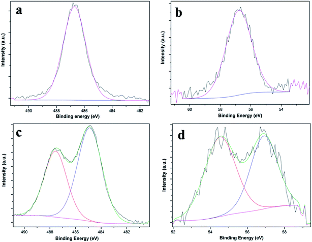
XPS measurements were performed for the electrodes before and after the electrochemical studies. Fig. 3a and b show the survey spectrum and high-resolution spectrum of Sn 3d5/2 before performing the electrochemical studies. The spectrum of Sn 3d5/2 was deconvoluted into two peaks at 486.7 eV and 484.8 eV for SnO2 and metallic tin, respectively. A small percentage of metallic tin might have accumulated during deposition.
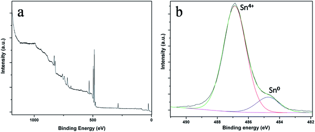 | ||
| Fig. 3 XPS spectra of SnO2NW@GNS electrodes before electrochemical cycles (a) survey scan of electrode, (b) high resolution spectrum of Sn 3d5/2. | ||
3.1. Electrochemical analysis
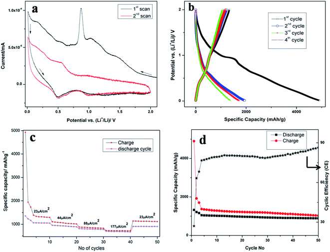
Fig. 4a shows the cyclic voltammetry (CV) curve of the first two cycles of SnO2NW@GNS at a scan rate of 0.05 mV s−1 in the potential range from 0.01 to 2.0 V. The first scan of Fig. 4a shows a broad peak in the range of 0.8 to 1.2 V and a sharp peak at 0.8 V arises from the broad peak. The broad peak may be attributed to the formation of SEI with the graphene sheet. The broad peak in the same range is also visible in the CV of GNS (graphene nanosheet) film alone on copper substrate (Fig. S3, ESI†). A small peak at ∼1.0 V (Fig. 4a) can be assigned to the conversion of SnO2 to SnO and Li2O,36,37 whereas, the sharp peak at 0.8 V (Fig. 4a) is attributed to the conversion of SnO2 to Sn and Li2O and the formation of SEI. The CV measurement of the GNS electrode demonstrates that the Li ion could intercalate and deintercalate into the graphene sheets. The Li insertion/deintercalation takes place at ≤0.1 V in the graphene sheets. The lithium ion insertion potential is quite low, very close to 0 V vs. the Li/Li+ reference electrode, whereas, the potential for lithium ion deintercalation is in the range 0.2–0.3 V.38Fig. 4b and c show galvanostatic charge–discharge cycles and the rate capability of the SnO2NW@GNS electrode. The first discharge and charge capacities are 1335 mAh g−1 and 4930 mAh g−1, respectively at a current density of 23 μA cm−2. The total capacity results from the contributions of SnO2 nanowires and graphene nanosheets. The much higher charge capacity is due to the GNS matrix. The high degree of defects in GNS may act as Li ion sites that contributed to a greater capacity. A large irreversible capacity loss of about 3600 mAh g−1 (73%) was observed for the sample at the first cycle. This huge irreversible capacity loss is due the irreversible reduction of SnO2 to Sn as described in eqn (1) and other irreversible processes such as decomposition of the electrolyte.39,40 During the second cycle, 64% of the charge capacity was retained for the discharge capacity, which was 1240 mAh g−1. Subsequent discharge cycles obtained 67% and 75% of the charge capacities. On the first charge, a flat plateau appeared around 0.8 V, which was attributed to the SEI formation. The charge–discharge profiles of SnO2 nanowires on copper substrates are given in S4 (ESI†). The first charge and discharge capacities were obtained as 2169 mAh g−1 and 828 mAh g−1, respectively, at a current density of 23 μA cm−2. About 62% of the irreversible capacity loss was observed in the first cycle, which was less than that of the SnO2NW@GNS electrode.
During the second cycle, about 89% of the charge capacity was retained for the discharge capacity. Only first cycles of charge–discharge capacities of various current densities were given in Fig. S5 of the ESI.† The irreversible decomposition of SnO2 to metallic tin surrounded by an amorphous, inactive Li2O matrix was ascribed to the SEI.41,42 The amorphous Li2O matrix allows Li ions to diffuse through and prevent the agglomeration of Sn atoms or LixSn alloy regions during volume changes.43 The rate performance of the electrode was evaluated at various current densities from 23 μA cm−2 to 177 μA cm−2. A coulombic efficiency of ∼87% was obtained for the SnO2NW@GNS electrode after 50 cycles at a current density of 23 μA cm−2 (Fig. 4d).
3.2. XPS and TEM studies after electrochemical performance
The XPS spectra corresponding to Sn 3d5/2 and Li 1s after the first charge cycle and discharge cycle are shown in Fig. 5a & c and b & d, respectively. After first charge, the spectra show a peak at 486.7 eV that can be attributed to the SnO2 phase. The Li 1s peak at 56.7 gives a Li2O phase of lithium. An alloy of SnO2 with Li may form and still retain some crystallinity. These have been confirmed from the TEM of the sample after the first charge cycle (Fig. 6b).A broad peak of Sn 3d5/2 is observed after the first discharge cycle (Fig. 5c). The peaks observed at 485.3 eV and 486.7 eV are assigned to Sn and Sn4+, respectively. The corresponding Li 1s peak also deconvoluted to two peaks at 54.6 and 56.3 eV (Fig. 5d) attributed to metallic lithium and the Li2O phase, respectively. The Li2O is an amorphous phase, which allows Li ions to pass through it and it is electrically insulating. XPS spectra of the electrode after the 50th cycle are presented in the ESI (S6†).
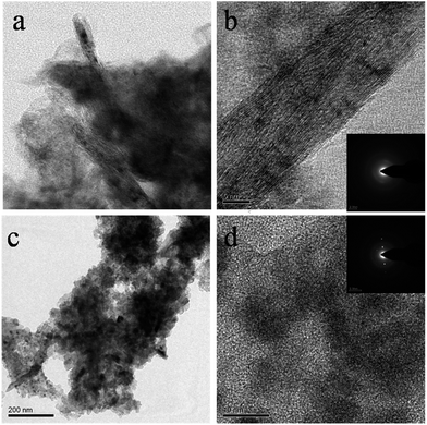
In order to understand the modifications that occur in the electrode during the charge/discharge process, an additional TEM study was carried out for the electrode after the charge cycle (after the first lithiation) and after the discharge cycle (after the first delithiation). Fig. 6a and b show TEM images of electrodes after the first charge state. The nanowire morphology of SnO2 was largely distorted and even a mild structure of nanowire can be seen in the TEM image (Fig. 6a). During charging, the formation of Li2O results in a large volume expansion in the nanowire.44 The high resolution TEM image of the electrode shows clear nanowire morphology and the SAED pattern (inset of Fig. 6b) shows retention of some degree of crystallinity of the nanowire during the first charged state. The lattice fringes have been changed when compared to the original SnO2 nanowire shown in Fig. 2d. After the discharge cycle, the complete morphology of SnO2 nanowires undergoes significant change and nanoparticles of Tin are formed (Fig. 6c). The HRTEM of tin particles shows crystalline nature and sizes of 5–10 nm. In the discharge process, the Li2O did not take part in electrochemical lithiation process and only LixSn nanoprecipitates were active in the lithiation process.
4. Conclusions
In summary, a 3-D heterogeneously nanostructured thin film was designed by uniformly anchoring SnO2 nanowires on the surface of a GNS matrix. This nanocomposite exhibited superior electrochemical performance, which was attributed to the morphology of the wires and the GNS matrix. The one-dimensional wires attached to the side walls of the GNS film increase the surface area of the active material for Li diffusion. The discharge capacity obtained was about 1335 mAh g−1 and the coulombic efficiency of ∼86% after the 50th cycle. Our studies demonstrate the potential opportunity for developing high-performance Li-ion batteries based on the GNS architecture composite. The present architecture of the anode material provides the concept of 3-D micro batteries. A stable 3-D framework of GNS supports SnO2 NWs without agglomeration, while graphene sheets play an important role in enhancing the conductivity of the electrode.References
- V. Etacheri, R. Marom, R. Elazari, G. Salitra and D. Aurbach, Energy Environ. Sci., 2011, 4, 3243 CAS.
- R. Marom, S. F. Amalraj, N. Leifer, D. Jacob and D. Aurbach, J. Mater. Chem., 2011, 21, 9938 RSC.
- Y. Idota, T. Kubota, A. Matsufuji, Y. Maekawa and T. Miyasaka, Science, 1997, 276, 1395 CrossRef CAS.
- J. B. Bates, G. R. Gruzalski, N. J. Dudney, C. F. Luck and X. H. Yu, Solid State Ionics, 1994, 70, 619 CrossRef.
- J. B. Bates, N. J. Dudney, D. C. Lubben, G. R. Gruzalski, B. S. Kwak, X. H. Yu and R. A. Zuhr, J. Power Sources, 1995, 54, 58 CrossRef CAS.
- H. Nishide and K. Oyaizu, Science, 2008, 319, 737 CrossRef CAS PubMed.
- A. Nathan, A. Ahnood, M. T. Cole, S. Lee, Y. Suzuki, P. Hiralal, F. Bonaccorso, T. Hasan, L. G. Gancedo, A. Dyadyusha, S. Haque, P. Andrew, S. Hofmann, J. Moultrie, D. Chu, A. Flewitt, A. Ferrari, M. Kelly, J. Robertson, G. Amaratunga and W. Milne, Proc. IEEE, 2012, 100, 1486 CrossRef.
- A. Patil, V. Patil, D. W. Shin, J. W. Choi, D. S. Paik and S. J. Y. Stacking, Mater. Res. Bull., 2008, 43, 1913 CrossRef CAS PubMed.
- K. Kanehori, K. Matsumoto, K. Miyauchi and T. Kudo, Solid State Ionics, 1983, 9–10, 1445 CrossRef CAS.
- X. Yu, J. B. Bates, G. E. Jellison and F. X. Hart, J. Electrochem. Soc., 1997, 144, 524 CrossRef CAS PubMed.
- J. H. Pikul, H. G. Zhang, J. Cho, P. V. Braun and W. P. King, Nat. Commun., 2013, 4, 1732 CrossRef PubMed.
- N. Mahmood, C. Zhang, H. Yin and Y. Hou, J. Mater. Chem. A, 2014, 2, 15 CAS.
- X. Song, J. Pan, L. Xiao, L. Gao and S. Mathur, Nanotechnology, 2013, 24, 205401 CrossRef PubMed.
- E. Kim, D. Son, T. G. Kim, J. Cho, B. Park, K. S. Ryu and S. H. Chang, Angew. Chem., Int. Ed., 2004, 43, 5984 CrossRef PubMed.
- M. Winter and J. O. Besenhard, Electrochim. Acta, 1999, 45, 31 CrossRef CAS.
- M. Wachtler, M. Winter and J. O. Besenhard, J. Power Sources, 2007, 105, 151 CrossRef.
- B. A. Boukamp, G. C. Lesh and R. A. Huggins, J. Electrochem. Soc., 1981, 128, 725 CrossRef CAS PubMed.
- X. W. Lou, Y. Wang, C. Yuan, J. Y. Lee and L. A. Archer, Adv. Mater., 2006, 18, 2325–2329 CrossRef CAS.
- C. K. Chan, H. L. Peng, G. Liu, K. McIlwrath, X. F. Zhang, R. A. Huggins and Y. Cui, Nat. Nanotechnol., 2008, 3, 31 CrossRef CAS PubMed.
- A. Magasinski, P. Dixon, B. Hertzberg, A. Kvit, J. Ayala and G. Yushin, Nat. Mater., 2010, 9, 353 CrossRef CAS PubMed.
- J. W. Zhu, S. Chen, X. D. Wu, Q. F. Han and X. Wang, ACS Nano, 2010, 4, 2822 CrossRef PubMed.
- M. S. Park, Y. M. Kang, J. H. Kim, G. X. Wang, S. X. Dou and H. K. Liu, Carbon, 2008, 46, 35 CrossRef CAS PubMed.
- J. Hassoun, F. Bonaccorso, M. Agostini, M. Angelucci, M. G. Betti, R. Cingolani, M. Gemmi, C. Mariani, S. Panero, V. Pellegrini and B. Scrosati, Nano Lett., 2014, 14(8), 4901 CrossRef CAS PubMed.
- H. Nishide and K. Oyaizu, Science, 2008, 319, 737 CrossRef CAS PubMed.
- A. R. Kamali and D. J. Fray, Rev. Adv. Mater. Sci., 2011, 27, 14 CAS.
- D. W. Kim, I. S. Hwang, S. J. Kwon, H. Y. Kang, K. S. Park, Y. J. Choi, K. J. Choi and J. G. Park, Nano Lett., 2007, 7, 3041 CrossRef CAS PubMed.
- Y. D. Ko, J. G. Kang, J. G. Park, S. Lee and D. W. Kim, Nanotechnology, 2009, 20, 455701 CrossRef PubMed.
- S. M. Paek, E. J. Yoo and I. Honma, Nano Lett., 2009, 9, 72 CrossRef CAS PubMed.
- J. Yao, X. P. Shen, B. Wang, H. K. Liu and G. X. Wang, Electrochem. Commun., 2009, 11, 1849 CrossRef CAS PubMed.
- J. O. Besenhard, J. Yang and M. Winter, J. Power Sources, 1997, 68, 87 CrossRef CAS.
- O. Mao, R. A. Dunlap and J. R. Dahn, J. Electrochem. Soc., 1999, 146, 405 CrossRef CAS PubMed.
- Z. Chen, M. Zhou, Y. Cao, X. Ai, H. Yang and J. Liu, Adv. Energy Mater., 2012, 2, 95 CrossRef CAS.
- M. S. Park, G. X. Wang, Y. M. Kang, D. Wexler, S. X. Dou and H. K. Liu, Angew. Chem., Int. Ed., 2007, 46, 750 CrossRef CAS PubMed.
- R. Thomas, K. Y. Rao and G. M. Rao, Electrochim. Acta, 2013, 108, 458 CrossRef CAS PubMed.
- Y. Y. Wu and P. D. Yang, J. Am. Chem. Soc., 2001, 123, 3165 CrossRef CAS.
- D. Wang, R. Kou, D. Choi, Z. Yang, Z. Nie, J. Li, L. V. Saraf, D. Hu, J. Zhang, G. L. Graff, J. Liu, M. A. Pope and I. A. Aksay, ACS Nano, 2010, 4, 1587 CrossRef CAS PubMed.
- W. Shi, J. Zhu, D. H. Sim, Y. Y. Tay, Z. Lu, X. Zhang, Y. Sharma, M. Srinivasan, H. Zhang, H. H. Hng and Q. Yan, J. Mater. Chem., 2011, 21, 3422 RSC.
- A. Kumar, A. L. M. Reddy, A. Mukherjee, M. Dubey, X. Zhan, N. Singh, L. Ci, W. E. Billups, J. Nagurny, G. Mital and P. M. Ajayan, ACS Nano, 2011, 5, 4345 CrossRef CAS PubMed.
- X. W. Lou, D. Deng, J. Y. Lee and L. A. Archer, Chem. Mater., 2008, 20, 6562 CrossRef CAS.
- M. S. Park, G. X. Wang, Y. M. Kang, D. Wexler, S. X. Dou and H. K. Liu, Angew. Chem., Int. Ed., 2007, 46, 750 CrossRef CAS PubMed.
- I. A. Courtney and J. R. Dahn, J. Electrochem. Soc., 1997, 144, 2045 CrossRef CAS PubMed.
- M. S. Park, G. X. Wang, Y. M. Kang, D. Wexler, S. X. Dou and H. K. Liu, Angew. Chem., 2007, 119, 764 CrossRef.
- A. Sivashanmugam, T. P. Kumar T, N. G. Renganathan, S. Gopukumar, M. M. Wohlfahrt and J. Garche, J. Power Sources, 2005, 144, 197 CrossRef CAS PubMed.
- J. Y. Huang, L. Zhong, C. M. Wang, J. P. Sullivan, W. Xu, L. Q. Zhang, S. X. Mao, N. S. Hudak, X. H. Liu, A. Subramanian, H. Fan, L. Qi, A. Kushima and J. Li, Science, 2010, 330, 1515 CrossRef CAS PubMed.
Footnote |
| † Electronic supplementary information (ESI) available. See DOI: 10.1039/c4ta04836a |
| This journal is © The Royal Society of Chemistry 2015 |

