Low-temperature MoO3 film from a facile synthetic route for an efficient anode interfacial layer in organic optoelectronic devices†
Jun
Liu
,
Xinkai
Wu
,
Sujie
Chen
,
Xingdong
Shi
,
Jing
Wang
,
Saijun
Huang
,
Xiaojun
Guo
and
Gufeng
He
*
National Engineering Lab for TFT-LCD Materials and Technologies, Department of Electronic Engineering, Shanghai Jiao Tong University, Shanghai 200240, People's Republic of China. E-mail: gufenghe@sjtu.edu.cn; Fax: +86 21 34204371; Tel: +86 21 34207045
First published on 16th October 2013
Abstract
A low temperature solution-processed MoO3 (sMoO3) thin film with a facile method for organic optoelectronic devices is developed. The film is extremely smooth with a root mean square (RMS) roughness of 0.318 nm, which is a significant advance for fabricating devices. An X-ray photoelectron spectroscopy (XPS) measurement shows that the sMoO3 possesses few Mo5+ states with a Mo![[thin space (1/6-em)]](https://www.rsc.org/images/entities/char_2009.gif) :O stoichiometry of 2.99, demonstrating a nearly ideal MoO3 stoichiometry at a low annealing temperature. The sMoO3 film exhibits a superior hole injection ability in both an organic light-emitting diode (OLED) and organic photovoltaic cell (OPV), compared to conventional hole injection material poly (3,4-ethylenedioxythiophene):poly(styrenesulfonate) (PEDOT:PSS). It is proved that the sMoO3 fabricated by the simple and low-cost method is an excellent alternative to a PEDOT:PSS anode buffer layer for solution-processed organic optoelectronic devices.
:O stoichiometry of 2.99, demonstrating a nearly ideal MoO3 stoichiometry at a low annealing temperature. The sMoO3 film exhibits a superior hole injection ability in both an organic light-emitting diode (OLED) and organic photovoltaic cell (OPV), compared to conventional hole injection material poly (3,4-ethylenedioxythiophene):poly(styrenesulfonate) (PEDOT:PSS). It is proved that the sMoO3 fabricated by the simple and low-cost method is an excellent alternative to a PEDOT:PSS anode buffer layer for solution-processed organic optoelectronic devices.
Introduction
In the last two decades, wide attention has been paid to solution-processed optoelectronic devices such as organic light-emitting diodes (OLEDs)1,2 and organic photovoltaic cells (OPVs),3,4 owing to their potential for realizing low-cost, light-weight, large-area and flexible devices. In order to enhance device efficiency and stability, an effective strategy is to obtain a significant energetic match at the electrode–organic interface, by inserting an interfacial layer.5,6 A commonly used hole-injection material is poly (3,4-ethylenedioxythiophene):poly(styrenesulfonate) (PEDOT:PSS). However, its acidic and hygroscopic nature is associated with the long-term instability.7–10 Moreover, the low work function (5.1 eV) of PEDOT:PSS limits charge injection into the hole-transporting material with a large ionization potential.11,12 One of the most promising alternatives is molybdenum oxide (MoO3) that exhibits non-toxicity and deep-lying electronic states.13–17 In particular, MoO3 as the hole injection layer (HIL) can be solution processed in view of low-cost and large-area production. Several precursors for fabricating a solution-processed MoO3 layer have been reported. Liu et al. spin coated an acidified aqueous ammonium heptamolybdate (NH4)6Mo7O24·H2O precursor solution on indium tin oxide (ITO) and heat treated this at 160 °C, to obtain a discontinuous coverage of MoO3 nanoparticles on the ITO surface.18 On the other hand, Murase et al. obtained a smooth MoO3 film by pre-heating the same precursor in deionized water before spin coating.19 Jasieniak et al. exploited oxomolybdate MoO2(acac)2 (acac = bis(2,4-pentanedionate)) as a precursor to develop a MoOx thin film, and the OPV using this as the modifying layer exhibits a comparable efficiency to that using a PEDOT:PSS modified anode. However, the current density–voltage (J–V) curve shows an s-shape, becoming more serious with increased annealing temperature, which requires a deeper understanding.20 The sol–gel technique provided another precursor, MoO2(OH)(OOH), by dissolving MoO3 powder in H2O2, but a high annealing temperature of 275 °C was required for the full conversion of the precursor to MoO3.21 A commercially available MoO3 nanoparticle precursor has also been spin coated, followed by a low annealing temperature of 100 °C, however, such an approach required oxygen plasma treatment to remove the polymer stabilizers.22 Recently, an aqueous MoO3 solution was prepared by dissolving MoO3 powder directly into deionized water, but extra heating (70 °C) and prolonged stirring were required when the solution concentration was higher than 0.1 wt%, and the root mean square (RMS) roughness of the MoO3 film was over 3 nm.23 Similarly, a MoO3 solution was obtained by dispersing molybdenum powder in ethanol and H2O2 mixed solvents, however, 18 hours reaction time was required and then the solution needed to be dried to solid molybdenum oxide, that was dispersed uniformly into ethanol.24Here, we present an ultra facile synthetic route for a low-temperature solution processed MoO3 anode buffer layer from an aqueous solution. The solution was prepared by dissolving MoO3 powder in ammonia–water to form a transparent ammonium molybdate solution without a further stirring or heating process. During the annealing process in air, the ammonium molybdate underwent rapid decomposition to MoO3, NH3 and H2O, the latter two components being volatile. The remaining MoO3 film completely covered the ITO surface with uniformly distributed nanoplates, and it possessed desirable surface electronic structures for hole injection. Such a solution-processed MoO3 (sMoO3) layer exhibits a superior hole injection property compared to evaporated MoO3 (eMoO3) and PEDOT:PSS, and its application in optoelectronic devices such as OLEDs and OPVs suggests that our simple technique provides an ideal approach to develop an effective MoO3 film as a HIL.
Results and discussions
As shown in Fig. 1, it is hard to dissolve MoO3 powder in deionized water, while it can be easily dissolved in ammonia–water at room temperature at ambient conditions. The aqueous transparent solution with MoO3 in ammonia–water is formed by the chemical reaction25 between MoO3, H2O and NH3 as follows| MoO3 + 2NH3 + H2O → (NH4)2MoO4. |
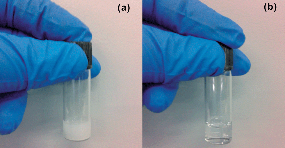 | ||
| Fig. 1 Photographs of solutions with MoO3 powder in deionized water (a) and ammonia–water (b). | ||
The ammonium molybdate (NH4)2MoO4 is soluble in H2O, and the solution is extremely stable and the properties do not change after 2 months storage in a refrigerating chamber at a temperature of 8 °C. The desired concentration is achieved by diluting a saturated solution (∼175 mg ml−1) into a certain amount of deionized water.
The aqueous MoO3 solution was spin coated onto a quartz glass substrate and annealed at 150 °C for 10 min in air. Fig. 2 shows atomic force microscopy (AFM) images of (a) the bare quartz glass, and the MoO3 films coated from solution with different concentrations: (b) 2, (c) 10 and (d) 20 mg ml−1. The bare quartz glass substrate exhibits a RMS roughness of 0.628 nm, with clear evidence of several particles stemming from sample contamination. The deposition of a MoO3 film on the quartz glass from a 2 mg ml−1 solution results in uniformly discrete nanoplates, which are formed by the aggregation of MoO3 nanoparticles. The diameter and height of the nanoplate are about 110 and 10 nm, respectively. However, the discontinuous coverage of the MoO3 nanoplates on the substrate causes a larger RMS roughness of 1.887 nm. By increasing the concentration of MoO3 in the ammonia–water, the density of the nanoplates increases, leading to a continuous and smooth sMoO3 film. The sMoO3 film coated from a 10 mg ml−1 solution exhibits a decreased RMS of 0.415 nm with retained tips of nanoplates. When the concentration increases to 20 mg ml−1, no single tip of MoO3 is observed and the RMS of the film is only 0.318 nm, indicating a homogeneous film covering the entire substrate. Furthermore, we have compared the optical transparency of the sMoO3 and PEDOT:PSS with a 10 nm thickness. As shown in Fig. S2,† the 10 nm sMoO3 film exhibits an ultra high transparency, better than PEDOT:PSS in the entire visible region. The obtained smooth surface morphology and extreme high transparency of the sMoO3 film are well suited for its employment in organic electronics.
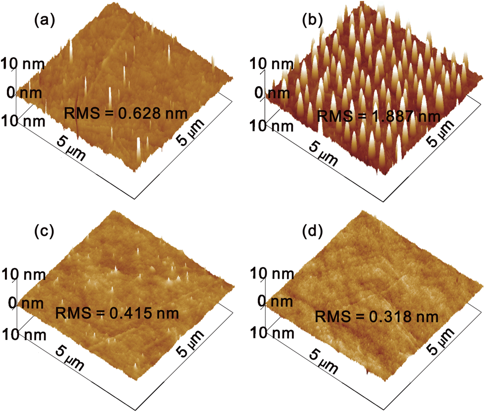 | ||
| Fig. 2 AFM images of bare quartz glass (a), and the sMoO3 films on quartz glass with 2 (b), 10 (c) and 20 (d) mg ml−1 solutions. | ||
X-ray photoemission spectroscopy (XPS) was performed to investigate the surface electronic structure of the sMoO3 films. Fig. 3a compares the full scan spectra of the eMoO3 and sMoO3 films. The characteristic peaks of the O 1s, Mo 3s, Mo 3p and Mo 3d levels in the full spectra of the eMoO3 film and the sMoO3 film are identical. Moreover, the peaks of the core levels of N are not found for the sMoO3 film, suggesting that the synthetic precursor containing the N element completely decomposes to MoO3 by annealing at the temperature of 150 °C. In Fig. 3b and c, the Mo 3d doublet has a spin–orbit splitting with 3.1 eV, between the Mo 3d3/2 and 3d5/2 bands. The Mo 3d3/2 and 3d5/2 peaks of the eMoO3 film locate at 232.9 and 236.0 eV, respectively, while those of the sMoO3 film locate at 233.0 and 236.1 eV, respectively. The higher binding energy of the solution processed sample is attributed to an increased adhesion between the sMoO3 film and the silicon substrate. To observe molybdenum in two different oxidation states, the Mo 3d spectra of the eMoO3 and sMoO3 films are fitted by two 3d doublets in the form of a Gaussian function. The calculated Mo5+/Mo6+ ratios for eMoO3 and sMoO3 are 0.058 and 0.019, respectively. By using the Mo5+/Mo6+ obtained from the Mo 3d core level spectra, the estimated Mo:O stoichiometries of eMoO3 and sMoO3 are 2.97 and 2.99, respectively. It can be seen that the concentration of the Mo5+ component in the eMoO3 film is significantly larger than that in the sMoO3 film, which coincides with the fact that preparation of MoO3 in the oxygen deficient environment leads to increased Mo5+ states, corresponding to the generation of oxygen vacancies. Therefore, fewer Mo5+ states are observed in the sMoO3 film from annealing in the air environment.
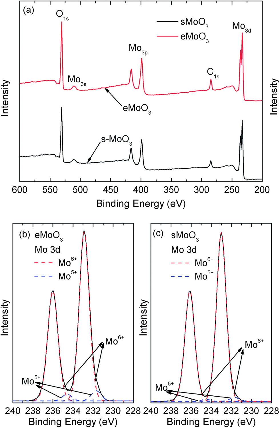 | ||
| Fig. 3 XPS spectra of the MoO3 films. (a) Full scanned spectra, Mo 3d core level of (b) eMoO3, and (c) sMoO3 prepared from a 20 mg ml−1 solution. | ||
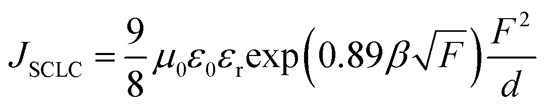
To elucidate the interfacial effect of sMoO3 as a HIL, hole-only devices with various hole injection materials were analyzed by means of the space-charge-limited current (SCLC). Fig. 4a shows the J–V characteristics of the hole-only devices with configuration of ITO/HIL (9000 rpm)/N,N′-diphenyl-N,N′-bis(1-naphthyl)-1,1′-biphenyl-4,4′′-diamine (NPB) (345 nm)/MoO3 (10 nm)/Al (100 nm). The theoretical JSCLC calculated from eqn (1).
 | (1) |
| ηINJ = JINJ/JSCLC | (2) |
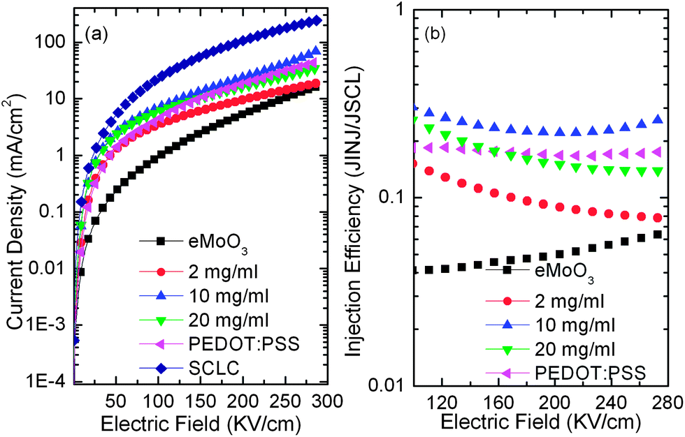 | ||
| Fig. 4 Current density versus electric field characteristics (a) and hole injection efficiency as a function of electric field (b) of hole-only devices with various HILs. | ||
The AFM image of the sMoO3 HIL from the 2 mg ml−1 solution shows a discontinuous film, leading to an unfavorable hole injection contact at the ITO–NPB interface, resulting in a moderate improvement of hole injection compared to the eMoO3 HIL. Moreover, a gradual damage of such a discontinuous film with an electric field28 might cause a serious roll-off of the injection efficiency, as depicted in Fig. 4b. However, the complete coverage of the sMoO3 HIL from the 10 mg ml−1 solution on ITO ensures a favorable and complete contact at the sMoO3–NPB interface, so that it has a dramatically enhanced hole injection efficiency, compared to the sMoO3 HIL from the 2 mg ml−1 solution and the PEDOT:PSS HIL, indicating the substitution of the sMoO3 HIL with optimum thickness for PEDOT:PSS. For the sMoO3 HIL from the 20 mg ml−1 solution, the device exhibits a reduced injection efficiency, due to the insulating nature of the thick sMoO3 layer with about a 10 nm thickness, which consumes voltages and leads to a slight roll-off of the injection efficiency with increasing electric field.
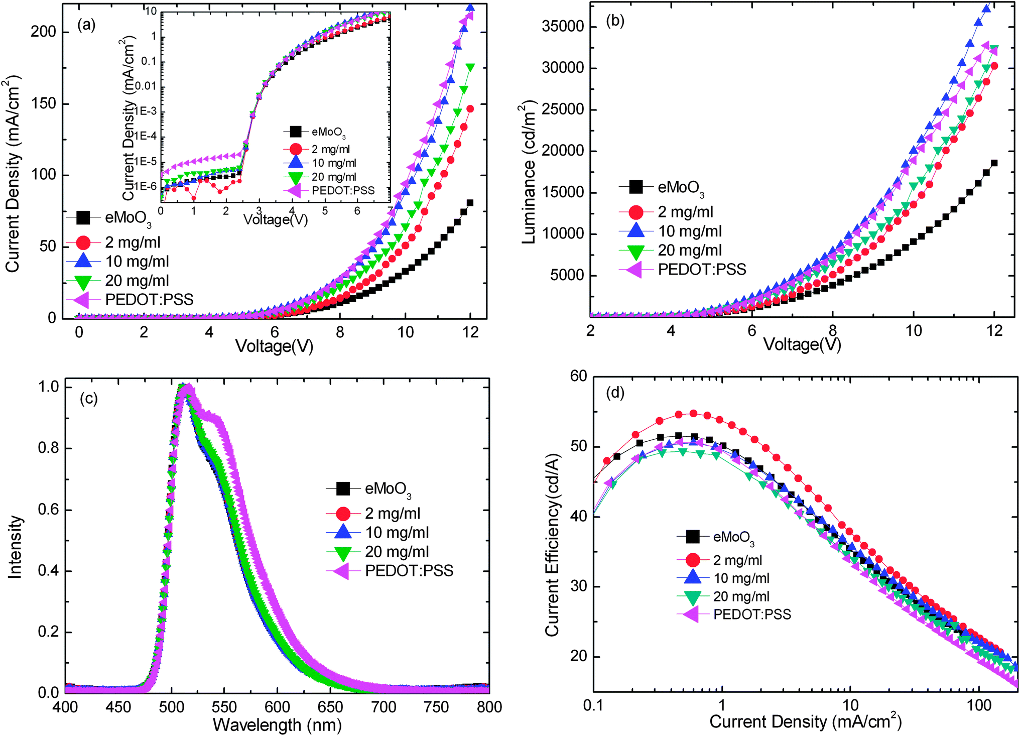
Five conventional green phosphorescent OLEDs using sMoO3 from 3 different concentrations, eMoO3 and PEDOT:PSS as HILs were examined, with the configuration ITO/HIL/NPB (35 nm)/CBP:Ir(ppy)3 (8%, 20 nm)/TPBI (60 nm)/LiF (0.5 nm)/Al (100 nm). Fig. 5a and b show the J–V and luminance–voltage (L–V) characteristics of the OLEDs with various HILs. Similar to the performance of the hole-only devices, the OLED with the sMoO3 HIL from the 10 mg ml−1 solution shows a higher current density than that with the sMoO3 HIL from the 2 and 20 mg ml−1 solutions and the eMoO3 HIL. Moreover, the OLED with the sMoO3 HIL exhibits a small leakage current, nearly one order of magnitude lower than that of the OLED with the PEDOT:PSS HIL.
 | ||
| Fig. 5 Current density–voltage (a), luminance–voltage (b), EL spectrum (c) and current efficiency–current density (d) characteristics of OLEDs with various HILs. | ||
Fig. 5c shows the electroluminescent (EL) spectra at a current density of 5 mA cm−2. Devices with the sMoO3 and eMoO3 HILs exhibit almost identical EL shapes with a minor difference of the intensity at 550 nm, while that with the PEDOT:PSS HIL shows an obviously higher shoulder at 550 nm, which may be due to the microcavity effect in the device. In Fig. 5d we present the current efficiency of devices with various HILs as a function of current density. Using the sMoO3 HIL from the 2 mg ml−1 solution, a maximum current efficiency of 54.8 cd A−1 was obtained. This efficiency is obviously better than the devices with the eMoO3 and PEDOT:PSS HILs. The enhancement of the efficiency is attributed to a more favorable hole injection and better balance of holes and electrons within the device with the sMoO3 HIL. However, further enhancing the hole injection will induce excessive hole carriers and therefore result in a carrier imbalance within the device. According to the analysis of hole-only devices, the sMoO3 HIL from solution with a high concentration exhibits a better hole injection than that from the 2 mg ml−1 solution. Therefore, the efficiency of the device with the sMoO3 HIL from the 10 or 20 mg ml−1 solution decreases.
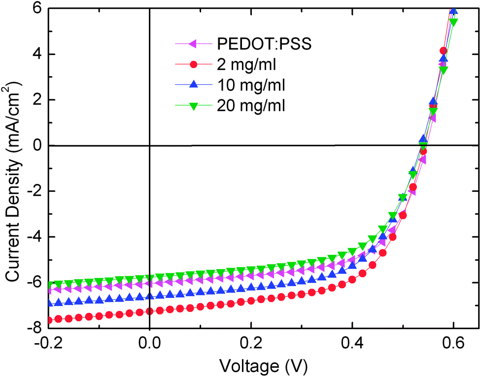
In addition to the application of the sMoO3 as HIL in OLEDs, the effect of this anode buffer layer as a HIL in an OPV with a poly(3-hexylthiophene):[6,6]-phenyl C61 butyric acid methyl ester bulk hetero junction (P3HT:PC61BM BHJ) system was also investigated. Fig. 6 depicts the J–V characteristics of the OPV devices using the sMoO3 and PEDOT:PSS HILs, and Table 1 summarizes the detailed results. The device with the sMoO3 HIL from the 2 mg ml−1 solution shows the best power conversion efficiency (PCE) of 2.35%, with an open-circuit voltage (VOC) of 0.54 V, a short-circuit current (JSC) of 7.26 mA cm−2, and a fill factor (FF) of 60.0%, which is better than that using the PEDOT:PSS HIL (PCE = 2.03%). According to the literature,20 an increase in the Mo5+ states in the sMoO3 induces the recombination of photogenerated holes and unfavorable interfacial dipoles, leading to a drop in JSC and the PCE. Therefore, the enhancement of the PCE in our experiment using sMoO3 from the 2 mg ml−1 solution is attributed to the reduced recombination, due to fewer Mo5+ states (Fig. 3) and enhanced hole collection through the sMoO3 layer. On the other hand, the sMoO3 layer from the 20 mg ml−1 solution is thick enough (about 10 nm) to reduce the JSC due to the insulating nature of MoO3, resulting in a decreased PCE to 1.84%. The application of the sMoO3 layer from the 2 and 20 mg ml−1 solutions in OPVs has the same trend in the variation of hole injection as that in the OLEDs. However, for the sMoO3 layer from the 10 mg ml−1 solution, its hole injection ability from ITO to NPB in the OLED is the best, while that from P3HT:PC61BM to ITO in the OPV declines. This difference may arise from the complicated sMoO3–NPB and sMoO3–P3HT:PC61BM interfacial energetic situations, such as interfacial dipole, charge transfer, sub-gap states. This issue requires a further understanding that is outside the scope of our work, and a detailed investigation is currently underway.
 | ||
| Fig. 6 Current density–voltage characteristic of P3HT:PC61BM OPV with sMoO3 and PEDOT:PSS HILs. | ||
| MoO3 solutions | V OC (V) | J SC (mA cm−2) | FF (%) | PCE (%) |
|---|---|---|---|---|
| 2 mg ml−1 | 0.54 | 7.26 | 60.0 | 2.35 |
| 10 mg ml−1 | 0.54 | 6.62 | 59.0 | 2.11 |
| 20 mg ml−1 | 0.54 | 5.77 | 59.1 | 1.84 |
| PEDOT:PSS | 0.54 | 6.03 | 62.2 | 2.03 |
Experimental
Preparation of the MoO3 solution: The MoO3 solution was prepared by rapidly dissolving MoO3 (422.8 mg) powder into ammonia–water (2.4 ml) without further stirring or a heating process. The saturated solution had a concentration of 175 mg ml−1, and it could be diluted by deionized water to the desired concentration.Characterization
The AFM images were obtained in room-temperature air by a Digital Instruments Multimode Nanoscope AFM with the tapping mode. The XPS test was carried out in a Kratos AXIS Ultra DLD ultrahigh vacuum surface analysis system with a monochromatic aluminum Kα source (1486.6 eV). For the AFM and XPS measurements, the sMoO3 films were deposited on quartz glass substrates and silicon substrates, respectively.Fabrication of OLEDs
OLEDs were fabricated on ITO-coated glass substrates. Prior to film deposition, the ITO glass substrates were cleaned successively using deionized water, acetone and isopropanol under an ultrasonic bath, then dried with nitrogen and pretreated with oxygen plasma. The sMoO3 layer was spin coated from the solution prepared above at 9000 rpm for 60 s and annealed at 150 °C for 20 min. The PEDOT:PSS (VP AI 4083 from H. C. Stark, PEDOT4083) layer was spin coated at 4000 rpm for 60 s and annealed at 150 °C for 10 min. The other organic layers were thermally deposited within a high vacuum deposition system at a base pressure of 10−6 Torr through a shadow mask. The active area defined by the overlap of the ITO anode and the Al cathode was 3 mm × 3 mm. The deposition rate for the organic materials was monitored by a quartz-crystal monitor. The doping of the organic layers was made by thermal co-evaporation, controlled via two separate quartz-crystal monitors. The J–V and L–V characteristics were measured with a computer controlled Keithley 2400 Source Meter and BM-7A Luminance Colorimeter under ambient conditions.Fabrication of OPV devices: the OPV devices were also fabricated on patterned ITO-coated glass substrates. The sMoO3 and PEDOT:PSS HILs were spin coated as above. The P3HT and PC61BM (1:1 weight ratio) solution dissolved in dichlorobenzene (20 mg ml−1) was spin coated at 600 rpm for 120 s and annealed at 150 °C for 10 min in a nitrogen glove box. Then, a 20 nm thick Ca and a 80 nm thick Al layer were thermally evaporated as a cathode under a vacuum at a base pressure of 1 × 10⁻⁶ Torr. The active area was 0.04 cm2. The J–V characteristics were measured by the Keithley 2400 Source Meter. The OPV performance was carried out using an Air Mass 1.5 Global (AM 1.5G) solar simulator with an irradiation intensity of 100 mW cm−2.
Conclusions
In summary, we have proposed a simple synthetic route of MoO3 anode buffer layer spin coated from an aqueous solution, which was prepared by rapidly dissolving MoO3 powder in ammonia–water without a long-time stirring or heating process. The solution enables an ultra-smooth MoO3 thin film with the appropriate electronic properties for hole injection in organic optoelectronic devices. A hole-only device study confirms that the sMoO3 from the optimum solution provides an excellent hole injection property compared to that using the conventional PEDOT:PSS and eMoO3. OLED and OPV devices utilizing the sMoO3-modified anodes have also been investigated. The device performance depends on the concentration of the precursor solution, and the highest current efficiency and PCE are realized with the sMoO3 HIL from a 2 mg ml−1 solution. In a word, the sMoO3 layer developed by the facile and low-cost technique is a feasible candidate for replacing the PEDOT:PSS anode buffer layer in organic electronics.Acknowledgements
This work was supported by the National Natural Science Foundation of China (61377030) and the Science and Technology Commission of Shanghai Municipal (11PJ1404900, 12JC1404900). The authors would like to thank Mrs Huiqin Li and Mrs Limin Sun from the Instrumental Analysis Center of the SJTU, for helping with the AFM and XPS measurements.Notes and references
- R. H. Friend, R. W. Gymer, A. B. Holmes, J. H. Burroughes, R. N. Marks, C. Taliani, D. D. C. Bradley, D. A. D. Santos, J. L. Bredas, M. Logdlund and W. R. Salaneck, Nature, 1999, 397, 121 CrossRef CAS PubMed.
- C. W. Tang and S. A. Van Slyke, Appl. Phys. Lett., 1987, 51, 913 CrossRef CAS.
- R. Steim, F. R. Kogler and C. J. Brabec, J. Mater. Chem., 2010, 20, 2499 RSC.
- H. Chen, J. Hou, S. Zhang, Y. Liang, G. Yang, Y. Yang, L. Yu, Y. Wu and G. Li, Nat. Photonics, 2009, 3, 649 CrossRef CAS.
- V. S. Gevaerts, A. Furlan, M. M. Wienk, M. Turbiez and R. A. J. Janssen, Adv. Mater., 2012, 24, 2130 CrossRef CAS PubMed.
- C. E. Small, S.-W. Tsang, J. Kido, S. K. So and F. So, Adv. Funct. Mater., 2012, 22, 3261 CrossRef CAS.
- M. Jorgensen, K. Norrman and F. C. Kreb, Sol. Energy Mater. Sol. Cells, 2008, 92, 686 CrossRef PubMed.
- M. P. de Jong, L. J. van Ijzendoorn and M. J. A. de Voigt, Appl. Phys. Lett., 2000, 77, 2255 CrossRef CAS.
- F. So and D. Kondakov, Adv. Mater., 2010, 22, 3762 CrossRef CAS PubMed.
- K. Norrman, M. V. Madsen, S. A. Gevorgyan and F. C. Krebs, J. Am. Chem. Soc., 2010, 132, 16883 CrossRef CAS PubMed.
- A. W. Hains and T. J. Marks, Appl. Phys. Lett., 2008, 92, 023504 CrossRef.
- K. R. Choudhury, J. Lee, N. Chopra, A. Gupta, X. Jiang, F. Amy and F. So, Adv. Funct. Mater., 2009, 19, 491 CrossRef CAS.
- Y. Sun, C. J. Takacs, S. R. Cowan, J. H. Seo, X. Gong, A. Roy and A. J. Heeger, Adv. Mater., 2011, 23, 2226 CrossRef CAS PubMed.
- D. Y. Kim, J. Subbiah, G. Sarasquesta, F. So, H. Ding, Irfan and Y. Gao, Appl. Phys. Lett., 2009, 95, 093304 CrossRef.
- Irfan, H. Ding, Y. Gao, C. Small, D. Y. Kim, J. Subbiah and F. So, Appl. Phys. Lett., 2010, 96, 243307 CrossRef.
- J. Qiu, Z. B. Wang, M. G. Helander and Z. H. Lu, Appl. Phys. Lett., 2011, 99, 153305 CrossRef.
- H. You, Y. Dai, Z. Zhang and D. Ma, J. Appl. Phys., 2007, 101, 026105 CrossRef.
- F. Liu, S. Shao, X. Guo, Y. Zhao and Z. Xie, Sol. Energy Mater. Sol. Cells, 2010, 94, 842 CrossRef CAS PubMed.
- S. Murase and Y. Yang, Adv. Mater., 2012, 24, 2459 CrossRef CAS PubMed.
- J. J. Jasieniak, J. Seifter, J. Jo, T. Mates and A. J. Heeger, Adv. Funct. Mater., 2012, 22, 2594 CrossRef CAS.
- C. Girotto, E. Voroshazi, D. Cheyns, P. Heremans and B. P. Rand, ACS Appl. Mater. Interfaces, 2011, 3, 3244 CAS.
- J. Meyer, R. Khalandovsky, P. Görrn and A. Kahn, Adv. Mater., 2011, 23, 70 CrossRef CAS PubMed.
- M.-F. Xu, L.-S. Cui, X.-Z. Zhu, C.-H. Gao, X.-B. Shi, Z.-M. Jin, Z.-K. Wang and L.-S. Liao, Org. Electron., 2013, 14, 657 CrossRef CAS PubMed.
- F. Xie, W. C. H. Choy, C. Wang, X. Li, S. Zhang and J. Hou, Adv. Mater., 2013, 25, 2051 CrossRef CAS PubMed.
- P. S. Patil and R. S. Patil, Bull. Mater. Sci., 1995, 18, 911 CrossRef CAS.
- H. Lee, S. W. Cho, K. Han, P. E. Jeon, C.-N. Whang, K. Jeong, K. Cho and Y. Yi, Appl. Phys. Lett., 2008, 93, 043308 CrossRef.
- M. Kröger, S. Hamwi, J. Meyer, T. Riedl, W. Kowalsky and A. Kahn, Appl. Phys. Lett., 2009, 95, 123301 CrossRef.
- C.-C. Chang, S.-W. Hwang, C. H. Chen and J.-F. Chen, Jpn. J. Appl. Phys., 2004, 43, 6418 CrossRef CAS.
Footnote |
| † Electronic supplementary information (ESI) available. See DOI: 10.1039/c3tc31580k |
| This journal is © The Royal Society of Chemistry 2014 |