The mechanism of graphene oxide as a growth template for complete reduced graphene oxide coverage on an SiO2 substrate†
Jingfeng
Huang
abc,
Derrick
Fam
a,
Qiyuan
He
a,
Hu
Chen
abc,
Da
Zhan
ad,
Steve H.
Faulkner
c,
Myra A.
Nimmo
bc and
Alfred Iing
Yoong Tok
*ab
aSchool of Materials Science and Engineering, Nanyang Technological University, Singapore 639798. E-mail: miytok@ntu.edu.sg; Tel: +65 67904935
bInstitute for Sports Research, Nanyang Technological University, 50 Nanyang Avenue, Singapore 639798
cSchool of Sport, Exercise and Health Sciences, Loughborough University, Leicestershire, LE113TU, UK
dSchool of Physical and Mathematical Sciences, Nanyang Technological University, Singapore 639798
First published on 22nd October 2013
Abstract
Reduced Graphene Oxide (rGO) has the distinct advantage of an aqueous and industrial-scalable production route. However large deviation in the electrical resistivity of fabricated rGO devices, caused by inhomogeneous coverage of rGO on the substrate, prevents its practical application in electronic devices. This critical problem could be solved by using an ethanol chemical vapour deposition (CVD) treatment on graphene oxide (GO). With the treatment, not only GO is reduced to rGO, but also rGO preferentially grows outwards from the edges of the existing GO template and enlarge in size until rGO completely covers the substrate. The growth sequence is presented and our results indicate that the growth supports the free radical condensate growth mechanism. After the ethanol CVD treatment, the standard deviation in electrical resistivity decreased significantly by 99.95% (1.60 × 10⁶ to 7.72 × 10² Ω per square) in comparison with hydrazine-reduced rGO substrates. As no carbon signatures on the substrate were observed when no template was used, this work indicates that GO could act as a template for subsequent formation of rGO.
1 Introduction
Graphene consists of a single planar layer of sp2 hybridised carbon. Its large carrier mobility and extraordinary optical, thermal and chemical properties have been in the spotlight1 since its exfoliation from graphite in 2004.2 However, the zero-band gap and semi-metal electronic structure of graphene confine its use in optical, electronic and sensing applications.3,4 Therefore, approaches have been made to open the band-gap, such as breaking inversion symmetry in bi-layer graphene,5 lateral confinement,6,7 strain engineering,8 oxidation9 and usage of reduced graphene oxide (rGO).10One of the methods to obtain the band-gap is to use rGO. This method is inexpensive and has an aqueous-processable route, thus making it compatible with many chemical processes and industrial-scalable. Despite these advantages and substantial interest in rGO research in recent years,11 synthesis of rGO on substrates with good homogeneity and conductivity for practical applications has not been reported.12 For device fabrication, rGO flakes have been spin-coated or attached electrostatically by (3-aminopropyl)triethoxysilane (APTES) to silicon dioxide (SiO2) substrates. APTES's electrostatic attraction to graphene oxide (GO) is a common technique used to obtain mono- or few-layer GO on the substrate.13–16 However, the surface coverage ranges from 60–80%.13,17–19 This is due to the cross-linked APTES20 and varying sizes of rGO flakes,10 posing a problem to work with rGO fabrication.
Large sized thin-films of single and few-layered graphene have recently been synthesized using atmospheric pressure ethanol chemical vapour deposition (CVD) on copper.21 Carbon nanotubes were synthesized using atmospheric pressure ethanol CVD using catalysts such as iron.22 However, the metal catalysts used in these processes pose a problem to be removed later and sheets grown with metal catalysts do not have extensive applications because of the undesirable characteristics of the residual catalyst material.
Most of these metal catalysts form metastable metal carbides at high temperature which have (i) high carbon solubility and (ii) high carbon diffusion rates. The principle of catalytic reaction is that the metal catalyst can act as both an electron donor and acceptor. Metal catalysts are required for graphene21 and carbon nanotube22 growth which allows ready exchange between the metal surface and carbon molecules. From computational studies, it has also been reported that the minimum energy growth mechanism of graphene sheets is by the sequential addition of carbon hexagons at the edges of the graphene sheet.23
Thus it is reasonable to hypothesize that GO, with its 2D electron gas properties,11 is also comparable with metal surfaces and could act as a catalyst for the growth of rGO, thus producing rGO on the substrate with good homogeneity and conductivity for practical applications.
2 Experimental
Large GO flakes in aqueous solution were synthesized as reported10,24 and electrostatically attached to the APTES-functionalized SiO2 substrates. Thereafter, these substrates were placed on a quartz holder and into the CVD tube. The furnace was first purged with argon gas at 300 sccm for 40 minutes to remove oxygen gas that might oxidise rGO into gaseous products. Argon gas was then adjusted to 100 sccm; hydrogen gas was turned on and set at 20 sccm. The gases passed through an ethanol bubbler which was kept at 0 °C while the furnace was set at 950 °C for 2 hours. After 2 hours, the furnace was switched off and the tube was left to cool slowly to room temperature.The ethanol CVD-treated chips were then characterized using (1) a JEOL JSM-7600F Field Effect Scanning Electron Microscope (SEM) instrument operating in gentle beam mode at 1 kV; (2) a FEI Tecnai F20 Transmission Electron Microscope (TEM) instrument operating at 200 kV for bright field imaging and a JEOL 2000FX TEM operating at 200 kV, beam size 130 nm, for SAED imaging; (3) a Keithley 4200-SCS semiconductor parameter analyser with 20 nm titanium and 100 nm gold electrodes; (4) a Renishaw Invia Ultra Violet (UV) Raman of 325 nm, spot size 1 μm with an aperture of 40×; (5) an Asylum Research AFP-3D Atomic Force Microscope (AFM) in tapping mode using an Olympus AC240TS Silicon tip under ambient conditions with a scanning rate of 0.2 Hz and (6) an Advanced Instrument Technology 4-Point Probe CMT-SR2000N with 1 mm probe spacing and 100 g spring constant.
3 Results and discussion
The experiment used an alcohol CVD setup as shown in Fig. 1. In theory, any hydrocarbon source such as methane, ethylene and ethanol could be used. However, liquid carbon sources such as ethanol are a safer alternative than gaseous hydrocarbons, which are extremely flammable and may form explosive mixtures with air. Thus ethanol was used as the carbon source.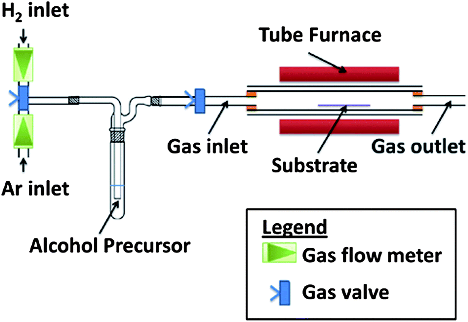 | ||
| Fig. 1 An atmospheric pressure CVD setup with alcohol vapors for growth of rGO. | ||
During the deposition phase, the gaseous hydrocarbon is thermally pyrolyzed: each of the C–C and C–H bonds could break to form two free radicals with each fragment keeping one electron. The presence of radicals in the molecule allows rapid rearrangement of carbon bonds. Though the reaction is more complicated for alcohols, the possible cracking of carbon radical species to form carbon deposition in the basic form could be expressed as eqn (1) and the catalytic hydrogenation25 process of solid carbon in which H2 forms CH4 as eqn (2).
| CxHy(g) ↔ xC(s) + (y/2)H2(g) | (1) |
| C(s) + 2H2(g) → CH4(g) | (2) |
According to Le Chatelier's principle and eqn (1), the growth rate of carbon will decrease with decreasing hydrocarbon concentration and increasing hydrogen gas. From eqn (2), increasing the ratio of hydrogen gas increases the dissociation rate of carbon and hydrogen into gaseous hydrocarbons. Thus the addition of hydrogen gas could help to etch away amorphous or excess carbon formed.26 In the experiment, by increasing the hydrogen to argon gas ratio from 0.17 to 0.34 while maintaining the total flow volume of the gas mixture, no deposition of carbon occurred even after 1 hour. With the ethanol precursor removed from the system for only 1 hour, no carbon Raman signature was detected on the substrate; the entire GO template was etched away. Thus, the deposition of rGO in the experiment obeys Le Chatelier's principle as depicted in eqn (1) and occurs in direct competition with the catalytic hydrogenation process as depicted in eqn (2).
In Fig. 2, the existing rGO flakes are highlighted in purple and the new growths are highlighted in yellow. Fig. 2a shows the GO coverage of ca. 60% after a typical APTES-functionalization and GO incubation on SiO2. However, after a partial ethanol CVD treatment for 30 minutes, the coverage increased to ca. 80% as shown in Fig. 2b. A high magnification of the new growth is shown in Fig. 2c. A lighter contrast was observed for the new growths compared with the existing GO flakes after the ethanol CVD treatment. The contrast difference could be due to the e-beam induced surface potential between graphene of different band gaps.27 The different thickness of the graphene could also be observed as different contrast, with darker sections indicating more layers.24 Thus SEM imaging allows efficient identification between the flakes and extensions after ethanol CVD treatment.
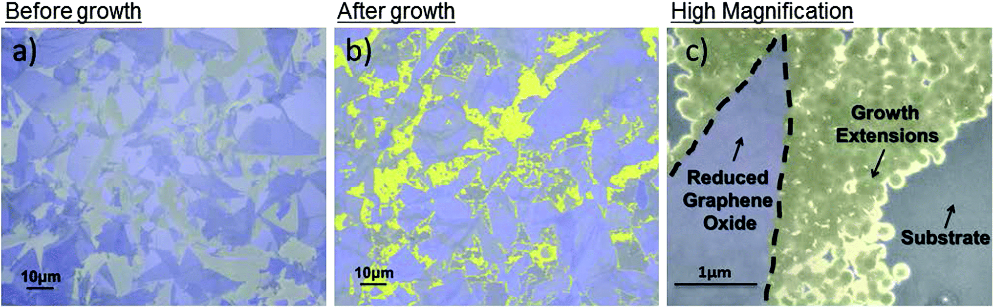 | ||
| Fig. 2 Scanning electron microscopy image of (a) before ethanol CVD treatment GO flakes with ca. 60% coverage and (b) after 30 minutes ethanol CVD treatment rGO flakes with ca. 80% coverage [GO flakes highlighted in purple and new growth highlighted in yellow]. (c) High-magnification image of the new growths. | ||
It is shown in the high-resolution SEM image that the rGO new growth can continue to act as a catalyst for subsequent growth, subsequently covering more of the gap between the existing rGO flakes. To prove the role of GO as an effective catalyst, substrates in the same conditions (clean and APTES-functionalized) without GO were processed under the same CVD conditions for up to 2 hours. Neither carbon deposits nor carbon spectra were detected by SEM and Raman spectroscopy respectively. Obviously the initial GO flakes act as crystal nuclei for the subsequent growth of these flakes.24
Since rGO can be a template for subsequent growth of rGO, this work supports the free radical condensate concept in which metal catalysts only help to initiate carbon precipitation and rearrangement at the nucleation stage: once the carbon structure is created, e.g. cloning of 1-dimensional carbon nanotubes,28 the metal catalyst becomes non-functional. The carbon radicals from the pyrolysis of ethanol could then catenate into longer chains by forming covalent bonds directly on the existing edges of the rGO template resulting in the growth observed.29
The 2 hour ethanol CVD processed film is then transferred onto lacey-carbon copper grids for TEM analysis. From the bright-field TEM image (Fig. S1a†), the new grown rGO, existing rGO and the boundary between these two regions are shown. The existing rGO region is characterized by the area with straight edges and darker contrast (thicker layers), while the new grown rGO has rounded edges and lighter contrast.
Selected area electron diffraction imaging (Fig. S1b†) on the film shows strong spots with a hexagonal pattern, confirming the three-fold symmetry arrangement of carbon atoms. There are weaker spots besides this set of hexagonal pattern forming a distinct weak ring-like pattern indicating that there are a few domains of crystalline graphene overlapped in the examined area. The first hexagonal ring pattern arises from the (100) plane while the second from the (110) plane.
To test the ethanol CVD processed rGO electrical properties, back-gated field-effect transistors based on 1 hour CVD processed GO sheets were fabricated and their electrical properties were tested under vacuum at room temperature. The channel length was 100 μm to ensure that transport is bulk-limited and the role of all contacts is minimized. Fig. 3a shows the drain current (Id) versus drain voltage (Vd) curve at six discrete gate voltages (Vg). The figure shows linear output behaviour indicative of a good ohmic contact between the GO film and electrodes. Fig. 3b illustrates the same transistor Id under sweeping Vg at fixed Vd = 0.1 V. The threshold voltage is shifted to the positive side due to p-doping from persistent moisture and oxygen. The CVD treated rGO device showed a clear increase in conductance as the Vg deviates from 0 V, indicating that the rGO films behaved as ambipolar semiconducting materials with stable electrical characteristics up to ±100 V.
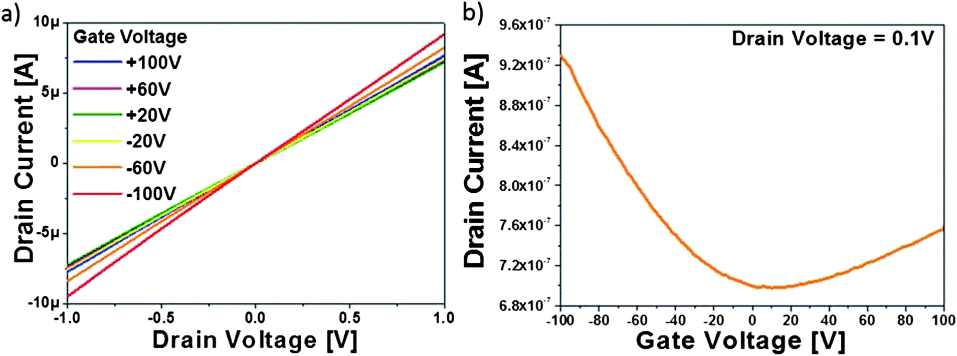 | ||
| Fig. 3 (a) Id–Vd (drain current–drain voltage) output graph under different applied gate voltages and (b) Id–Vg (drain current–gate voltage) transfer curve under sweeping gate voltages; of the CVD-processed rGO device under vacuum and room temperature. | ||
Hole mobility is obtained from the linear regime of the transfer curve using eqn (3), where L and W are the channel length and width; Cox is the gate capacitance; Vd, Vg and Id are the drain–source voltage, gate voltage and drain–source current respectively.
| μ = (L/WCoxVd)(ΔId/ΔVg) | (3) |
The hole mobility of a typical 2 hour ethanol CVD processed device under vacuum at room temperature is 124 cm2 V−1 s−1. It is considerably more than the rGO samples studied previously,30,31 thus validating that the CVD new growth could extend to the pre-existing 2-dimensional network and allows π-electron charge percolation.
The UV Raman spectra were obtained and fitted with Lorentzian function to obtain the positions and intensities of the peaks for the 15 min, 30 min, 60 min, 120 min ethanol CVD processed samples with diamond, GO, HOPG as comparison as shown in Fig. 4. UV Raman spectroscopy is used because in visible Raman spectroscopy, the sp2 sites have such a high cross-section that they dominate the spectra. The presence of G peaks in UV excitation of GO, rGO and HOPG showed that the sp2 vibrations still dominate even in the UV Raman excitation. The diamond sample exhibited a characteristic diamond peak at 1330 cm−1.32 For CVD processed rGO, the D peak was measured at 1409 cm−1 and the G peak at 1584 cm−1 in agreement with the existing literature.24,33,34
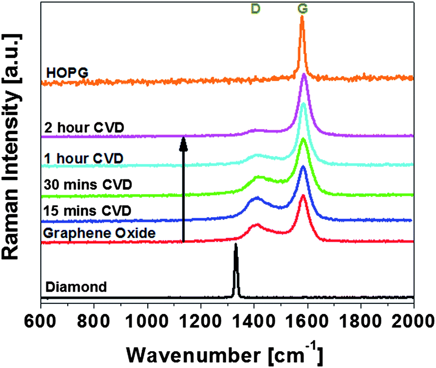 | ||
| Fig. 4 Ultra-violet Raman spectra of diamond, GO, different ethanol CVD processed rGO and HOPG. The intensities of diamond and HOPG are scaled down to allow fitting into the graph. | ||
We then investigate whether the grown carbon is rGO-like carbon or diamond-like carbon (DLC). RGO is defined generally as sp2 regions in an sp3 matrix whereas DLC is defined as amorphous carbon with sp3 and trans-polyacetylene bonds.33 The T peak33 that is due to C–C sp3 vibrations occurs only with UV Raman excitation at a wavenumber of ∼1060 cm−1. It is due to a resonant enhancement of the σ states and it directly probes the sp3 bonding. As the sp3 content falls, the sp3 vibrational density of states peak at 1060 cm−1 will shift upwards to that of sp2 VDOS at 1400 cm−1.33 In both GO and CVD processed rGO spectra, no T peak was observed, indicating that the CVD processed samples' sp3 percentage was small and non-diamond like. It is also observed that the D peak decreases as the CVD processing time increases, indicating increasing graphitic order in the rGO structure.35
The ID/IG ratio of the UV Raman excitation (Table 1) can be used to estimate the sp2 domain size using the Tuinstra–Koenig empirical formula36 under UV conditions.33 The ratio decreases continuously from 0.42 in the GO sample to 0.09 in the 2 hour CVD treated samples indicating that increased ethanol CVD treatment results in increased sp2 domain size in the rGO samples. Thus from Raman spectra and ID/IG, we confirm the carbon growth to be rGO, that the CVD treatment increases graphitization and that the sp2 domain size increases with increasing processing time. The Raman mapping of the intensity peaks of D, G and D/G is presented in Fig. S2.† The ID/IG ratio of the new grown rGO is lower than those of the existing rGO flakes indicating that the new grown rGO has larger sp2 domain size.
| GO | 15 min CVD | 30 min CVD | 1 hour CVD | 2 hour CVD | 12 hour hydrazine10 | ||
|---|---|---|---|---|---|---|---|
| UV Raman spectroscopy | Peak intensity of D/G | 0.42 | 0.35 | 0.32 | 0.17 | 0.09 | NA |
| AFM height profile | Flake thickness (nm) | 1.4 | 1.5 | 2 | 4 | 4 | NA |
| New growth thickness (nm) | 0 | 0 | 0.8 | 1 | 2 | NA | |
| 4-point probe sheet resistance (n = 5) | Average resistance (Ω □−1) | NA | 6.10 × 10⁴ | 2.87 × 10⁴ | 2.23 × 10⁴ | 4.68 × 10³ | 1.99 × 10⁶ |
| Standard deviation (Ω □−1) | NA | 4.43 × 10⁴ | 1.25 × 10⁴ | 7.16 × 10³ | 7.72 × 10² | 1.60 × 10⁶ | |
| Relative standard deviation (%) | NA | 72.6 | 43.6 | 32.1 | 16.5 | 80.5 | |
The AFM is performed on the 15 min, 30 min, 60 min, 120 min ethanol CVD processed samples. From 0 to 15 minutes of CVD treatment, the AFM height profile indicates that the thickness of the pre-existing GO template had a negligible increase in height and no growth from the edges was observed.26 However, as the process time increases to 30 minutes, new growths appear and the thickness of the GO template also increases slightly by 0.5 nm. With increasing process time to 2 hours, the new growths continue to extend outwards and completely cover the gaps in between the pre-existing rGO flakes. The new growth thickness after 2 hours of growth is 2 nm and this corresponds to ∼2–3 layers of rGO.10 The AFM image and the corresponding height profile between the existing rGO and the new grown rGO of a 2 hour CVD treated sample are shown in Fig. S3.†
From the 4-point probe measurement, the average electrical resistance of the chips decreased from 1.99 × 10⁶ to 4.68 × 10³ Ω per square (99.76% reduction) while the relative standard deviation decreased from 1.60 × 10⁶ to 7.72 × 10² Ω per square (99.95% reduction) after a 2 hour ethanol CVD treatment as compared to 12 hour hydrazine vapor reduction. The decrease in electrical resistivity in the ethanol CVD treated samples could be attributed to the increased percolation pathways between flakes due to the new growth completely filling up gaps between the pre-existing rGO flakes. Due to the more uniform and increased coverage of the rGO on the substrate, the reported growth method had decreased the standard deviations between chips, thus solving a critical problem for the practical use of rGO in electronic devices.
Having considered the data from the experiment, we arrived at the following growth sequence of rGO schematic (Fig. 5). Ethanol CVD treatment of up to 15 minutes on the GO leads to an improved graphitization from the free radicals produced from pyrolysis of gaseous ethanol. After 30 minutes, a thin graphitic shell is formed around the GO catalyst. Due to the lower growth activation energy at the edge of graphene sheets for sequential addition of carbon hexagons,23 rGO preferentially grows out from the edges. Finally, rGO completely covers the substrate after 2 hours of the ethanol CVD growth process.
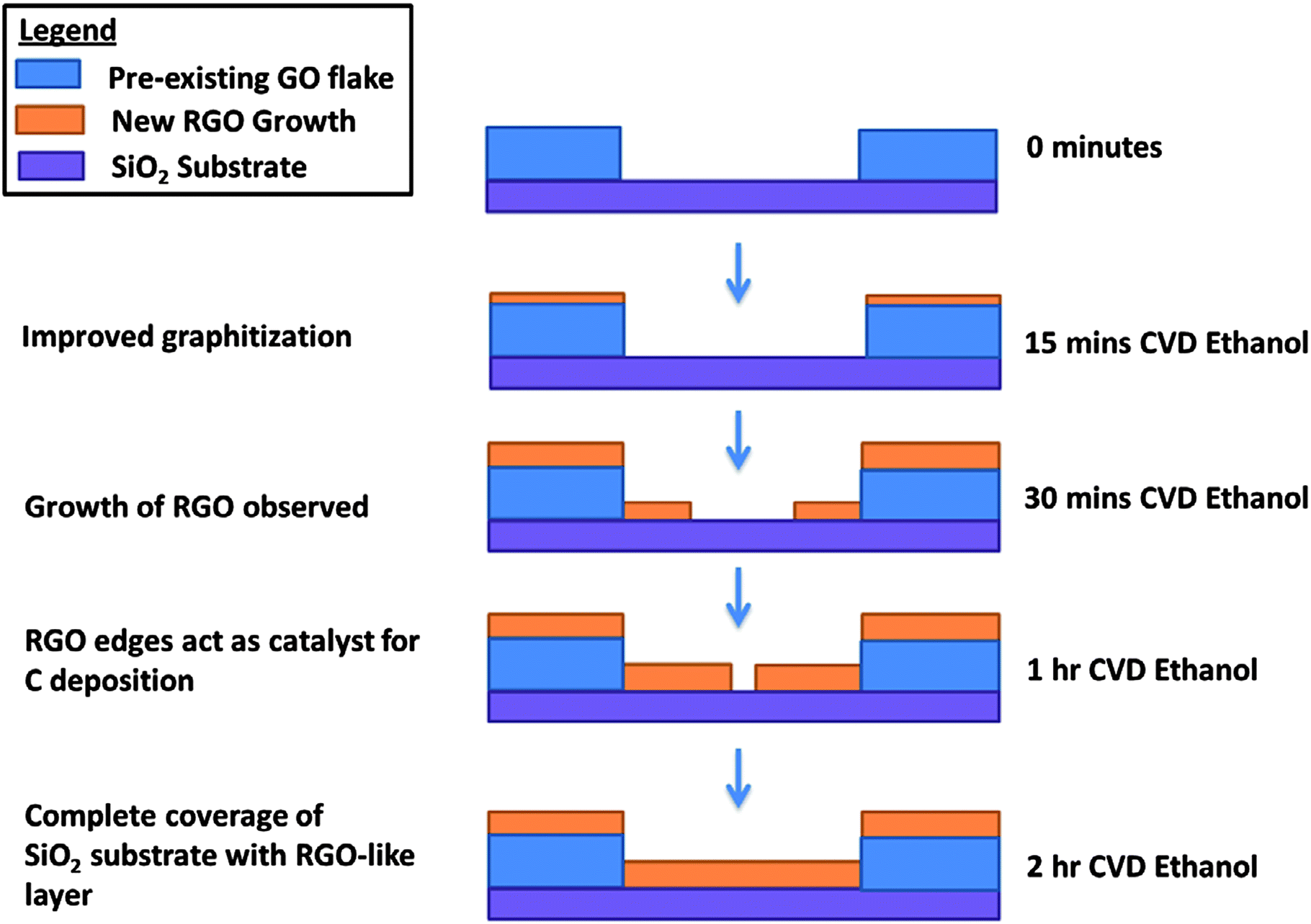 | ||
| Fig. 5 Schematic showing the growth sequence of rGO from a GO template during ethanol CVD treatment. | ||
Our data suggest that rGO could be grown via the free radical condensate mechanism. The mechanism of carbon nanotube carbon growth has been debated and two different mechanisms have been proposed: the dissolution of elemental carbon into metal nano-clusters followed by precipitation37 or the free radical condensate that carbon can act as a reaction medium for production of nanotubes.25 In the experiment, no metal catalyst was used, but rGO growth was observed, thus supporting the free radical condensate growth theory. After the pyrolysis of ethanol, free radicals preferentially condensate at the edges of the pre-existing GO flakes and thus rearrange themselves into a new carbon skeleton until a local minimum is reached.
4 Conclusions
Complete coverage of rGO on an SiO2 substrate was achieved using a GO template under ethanol CVD at ambient pressure without any metal catalysts. GO edges preferentially act as a catalyst for further growth of rGO. The growth sequence proceeds by the free radical condensate growth mechanism. After a 2 hour ethanol CVD treatment, the electrical resistivity decreased by 99.76% and its relative standard deviation decreased by 99.95% compared to hydrazine treated samples. The results and the proposed mechanism show that the use of 2 hour ethanol CVD treatment on GO is a promising way towards a better and homogeneous rGO for practical, high-yielding preparation of novel functional biosensors,38,39 catalysts,40 electronics,41 batteries42 or crystal growth templates.43Acknowledgements
The research was funded by the Institute for Sports Research (ISR) of Nanyang Technological University (NTU). The research was also partly supported by the National Institute for Health Research (NIHR) Diet, Lifestyle & Physical Activity Biomedical Research Unit based at University Hospitals of Leicester and Loughborough University. The views expressed are those of the authors and not necessarily those of the NHS, the NIHR or the Department of Health. The authors would like to thank Alagappan Palaniappan, Melanie Larisika, and Christoph Nowak from NTU's Centre for Biomimetic Sensor Science (CBSS) for aiding with the ethanol CVD setup and Zhou Zhaoxia from Loughborough Materials Characterisation Centre (LMCC) for aiding with the TEM instrument.Notes and references
- X. Huang, Z. Yin, S. Wu, X. Qi, Q. He, Q. Zhang, Q. Yan, F. Boey and H. Zhang, Small, 2011, 7, 1876–1902 CrossRef CAS PubMed.
- K. S. Novoselov, A. K. Geim, S. V. Morozov, D. Jiang, Y. Zhang, S. V. Dubonos, I. V. Grigorieva and A. A. Firsov, Science, 2004, 306, 666–669 CrossRef CAS PubMed.
- Q. Tang, Z. Zhou and Z. Chen, Nanoscale, 2013, 5, 4541–4583 RSC.
- S. H. Faulkner, R. A. Ferguson, N. Gerrett, M. Hupperets, S. G. Hodder and G. Havenith, Med. Sci. Sports Exercise, 2013, 45, 359–365 CrossRef PubMed.
- T. Ohta, A. Bostwick, T. Seyller, K. Horn and E. Rotenberg, Science, 2006, 313, 951–954 CrossRef CAS PubMed.
- M. Y. Han, B. Özyilmaz, Y. Zhang and P. Kim, Phys. Rev. Lett., 2007, 98, 206805 CrossRef.
- X. Zhou, C. M. Shade, A. L. Schmucker, K. A. Brown, S. He, F. Boey, J. Ma, H. Zhang and C. A. Mirkin, Nano Lett., 2012, 12, 4734–4737 CrossRef CAS PubMed.
- S. B. Cho and Y.-C. Chung, J. Mater. Chem. C, 2013, 1, 1595–1600 RSC.
- M. Z. Hossain, J. E. Johns, K. H. Bevan, H. J. Karmel, Y. T. Liang, S. Yoshimoto, K. Mukai, T. Koitaya, J. Yoshinobu, M. Kawai, A. M. Lear, L. L. Kesmodel, S. L. Tait and M. C. Hersam, Nat. Chem., 2012, 4, 305–309 CrossRef CAS PubMed.
- M. Larisika, J. Huang, A. Tok, W. Knoll and C. Nowak, Mater. Chem. Phys., 2012, 136, 304–308 CrossRef CAS PubMed.
- J. Huang, M. Larisika, C. Nowak and I. Y. A. Tok, New Methods in Aqueous Graphene (Graphene Oxide) Synthesis for Biosensor Devices, Taylor & Francis Group, Oxford, UK, 2013 Search PubMed.
- C.-Y. Su, Y. Xu, W. Zhang, J. Zhao, X. Tang, C.-H. Tsai and L.-J. Li, Chem. Mater., 2009, 21, 5674–5680 CrossRef CAS.
- Q. He, H. G. Sudibya, Z. Yin, S. Wu, H. Li, F. Boey, W. Huang, P. Chen and H. Zhang, ACS Nano, 2010, 4, 3201–3208 CrossRef CAS PubMed.
- Q. He, S. Wu, S. Gao, X. Cao, Z. Yin, H. Li, P. Chen and H. Zhang, ACS Nano, 2011, 5, 5038–5044 CrossRef CAS PubMed.
- J. Huang, J. Harvey, H. Chen, S. Faulkner, J. King, M. A. Nimmo and I. Y. A. Tok, icSPORTS 2013–Proc. Int. Congr. on Sport Sci. Res., 2013, 1, 83–88 Search PubMed.
- J. Huang, J. Harvey, W. H. D. Fam, M. A. Nimmo and I. Y. A. Tok, Procedia Eng., 2013, 60, 195–200 CrossRef CAS PubMed.
- Z. Wang, X. Zhou, J. Zhang, F. Boey and H. Zhang, J. Phys. Chem. C, 2009, 113, 14071–14075 CAS.
- S. Wu, Z. Yin, Q. He, G. Lu, Q. Yan and H. Zhang, J. Phys. Chem. C, 2011, 115, 15973–15979 CAS.
- S. Wu, Z. Yin, Q. He, G. Lu, X. Zhou and H. Zhang, J. Mater. Chem., 2011, 21, 3467–3470 RSC.
- A. Saini, S. Faulkner, N. Al-Shanti and C. Stewart, Ageing Res. Rev., 2009, 8, 251–267 CrossRef CAS PubMed.
- X. Dong, P. Wang, W. Fang, C.-Y. Su, Y.-H. Chen, L.-J. Li, W. Huang and P. Chen, Carbon, 2011, 49, 3672–3678 CrossRef CAS PubMed.
- J. H. Hafner, M. J. Bronikowski, B. R. Azamian, P. Nikolaev, A. G. Rinzler, D. T. Colbert, K. A. Smith and R. E. Smalley, Chem. Phys. Lett., 1998, 296, 195–202 CrossRef CAS.
- S. Haghighatpanah, A. Börjesson, H. Amara, C. Bichara and K. Bolton, Phys. Rev. B: Condens. Matter Mater. Phys., 2012, 85, 205448 CrossRef.
- J. Huang, M. Larisika, W. H. D. Fam, Q. He, M. A. Nimmo, C. Nowak and I. Y. A. Tok, Nanoscale, 2013, 5, 2945–2951 RSC.
- P. T. A. Reilly and W. B. Whitten, Carbon, 2006, 44, 1653–1660 CrossRef CAS PubMed.
- C.-Y. Su, Y. Xu, W. Zhang, J. Zhao, A. Liu, X. Tang, C.-H. Tsai, Y. Huang and L.-J. Li, ACS Nano, 2010, 4, 5285–5292 CrossRef CAS PubMed.
- J. Li, Y. He, Y. Han, K. Liu, J. Wang, Q. Li, S. Fan and K. Jiang, Nano Lett., 2012, 12, 4095–4101 CrossRef CAS PubMed.
- Y. Yao, C. Feng, J. Zhang and Z. Liu, Nano Lett., 2009, 9, 1673–1677 CrossRef CAS PubMed.
- S. Dutta and S. K. Pati, J. Mater. Chem., 2010, 20, 8207–8223 RSC.
- G. Eda, G. Fanchini and M. Chhowalla, Nat. Nanotechnol., 2008, 3, 270–274 CrossRef CAS PubMed.
- S. Wang, P. K. Ang, Z. Wang, A. L. L. Tang, J. T. L. Thong and K. P. Loh, Nano Lett., 2009, 10, 92–98 CrossRef PubMed.
- K. Okada, H. Kanda, S. Komatsu and S. Matsumoto, J. Appl. Phys., 2000, 88, 1674–1678 CrossRef CAS.
- A. C. Ferrari and J. Robertson, Phys. Rev. B: Condens. Matter Mater. Phys., 2001, 64, 075414 CrossRef.
- I. Calizo, I. Bejenari, M. Rahman, G. Liu and A. A. Balandin, J. Appl. Phys., 2009, 106, 043509 CrossRef.
- A. C. Ferrari, Mater. Res. Soc. Symp. Proc., 2001, 675, W11.5.1–W115.5.12 CrossRef CAS PubMed.
- F. Tuinstra and J. L. Koenig, J. Chem. Phys., 1970, 53, 1126–1130 CrossRef CAS.
- J. Gavillet, A. Loiseau, F. Ducastelle, S. Thair, P. Bernier, O. Stéphan, J. Thibault and J. C. Charlier, Carbon, 2002, 40, 1649–1663 CrossRef CAS.
- X. Teng, Y. Zhu, W. Wei, S. Wang, J. Huang, R. Naccache, W. Hu, A. I. Y. Tok, Y. Han, Q. Zhang, Q. Fan, W. Huang, J. A. Capobianco and L. Huang, J. Am. Chem. Soc., 2012, 134, 8340–8343 CrossRef CAS PubMed.
- S. M. Tan, H. L. Poh, Z. Sofer and M. Pumera, Analyst, 2013, 138, 4885–4891 RSC.
- L. Lai, J. R. Potts, D. Zhan, L. Wang, C. K. Poh, C. Tang, H. Gong, Z. Shen, J. Lin and R. S. Ruoff, Energy Environ. Sci., 2012, 5, 7936–7942 CAS.
- L. Huang, B. Wu, G. Yu and Y. Liu, J. Mater. Chem., 2011, 21, 919–929 RSC.
- W. Zhang, J. Zhu, H. Ang, Y. Zeng, N. Xiao, Y. Gao, W. Liu, H. H. Hng and Q. Yan, Nanoscale, 2013, 5, 9651–9658 RSC.
- X. Huang, S. Li, S. Wu, Y. Huang, F. Boey, C. L. Gan and H. Zhang, Adv. Mater., 2012, 24, 979–983 CrossRef CAS PubMed.
Footnote |
| † Electronic supplementary information (ESI) available: AFM image with corresponding height profile; optical microscopy image with Raman mapping of the intensities of D, G and D/G peaks; and bright-field TEM image with the SAED pattern of the 2 hour ethanol CVD processed sample. See DOI: 10.1039/c3tc31529k |
| This journal is © The Royal Society of Chemistry 2014 |