High work-function hole transport layers by self-assembly using a fluorinated additive†
Scott A.
Mauger‡
a,
Jun
Li
a,
Özge Tüzün
Özmen
b,
Andy Y.
Yang
a,
Stephan
Friedrich
c,
M. Diego
Rail
d,
Louise A.
Berben
d and
Adam J.
Moulé
*a
aDepartment of Chemical Engineering and Materials Science, University of California, Davis, CA 95616, USA. E-mail: amoule@ucdavis.edu; Fax: +1-530-752-1031; Tel: +1-530-754-8669
bDepartment of Physics, Düzce University, 81620 Düzce, Turkey
cAdvanced Detector Group, Lawrence Livermore National Laboratory, Livermore, CA 94550, USA
dDepartment of Chemistry, University of California, Davis, CA 95616, USA
First published on 30th October 2013
Abstract
The hole transport polymer poly(3,4-ethylenedioxythiophene):poly(4-styrenesulfonate) (PEDOT:PSS) derives many of its favorable properties from a PSS-rich interfacial layer that forms spontaneously during coating. Since PEDOT:PSS is only usable as a blend it is not possible to study PEDOT:PSS without this interfacial layer. Through the use of the self-doped polymer sulfonated poly(thiophene-3-[2-(2-methoxyethoxy) ethoxy]-2,5-diyl) (S-P3MEET) and a polyfluorinated ionomer (PFI) it is possible to compare transparent conducting organic films with and without interfacial layers and to understand their function. Using neutron reflectometry, we show that PFI preferentially segregates at the top surface of the film during coating and forms a thermally-stable surface layer. Because of this distribution we find that even small amounts of PFI increase the electron work function of the hole transport layer. We also find that annealing at 150 °C and above reduces the work function compared to samples heated at lower temperatures. Using near edge X-ray absorption fine structure spectroscopy and gas chromatography we show that this reduction in work function is due to S-P3MEET being doped by PFI. Organic photovoltaic devices with S-P3MEET/PFI hole transport layers yield higher power conversion efficiency than devices with pure S-P3MEET or PEDOT:PSS hole transport layers. Additionally, devices with a doped interface layer of S-P3MEET/PFI show superior performance to those with un-doped S-P3MEET.
1 Introduction
Organic photovoltaics (OPV) is a promising technology that has the potential to provide inexpensive, renewable energy and is deployable in locations and economies where the use of bulkier and more expensive inorganic photovoltaics is not feasible.1 One of the factors that currently limits their commercial success is low power conversion efficiency (PCE). Although champion devices have been produced with PCE values over 12%,2 module efficiency is lower. One of the methods researchers are currently studying to further improve PCE is to increase the open circuit voltage (VOC). Two successful strategies for improving VOC are adjusting the energy levels of the donor and acceptor materials3–7 or by engineering the interfaces between layers.8–13 In this paper we focus on the latter of these two approaches, specifically engineering the hole transport layer between the anode and the active layer. Engineering of the active layer/cathode interface has also proven successful in increasing VOC, with a variety of materials and methods available in the literature.8–12The most widely used hole transport layer (HTL) material is the copolymer blend poly(3,4-ethylenedioxythiophene):poly(styrene sulfonate) (PEDOT:PSS). In addition to PEDOT:PSS, semiconducting metal oxides such as V2O5, MoO3, and NiO have shown comparable efficiencies to PEDOT:PSS devices.14–16 The success of a metal oxide HTL relies on matching its electron work function (Φ) to the ionization potential (IP) of the donor material. In contrast to metal oxides, work function matching is not as critical with PEDOT:PSS as it has been shown to form lower than expected injection barriers and can accept holes from the highest occupied molecular orbital (HOMO) of any polymer.17 These unique properties of PEDOT:PSS are generally believed to be due the thin PSS-rich skin that forms on the top of the layer. This surface layer is important for device performance because it results in unfilled states at the Fermi level and prevents large interfacial barriers from forming with adjacent organic layers.18 We have also shown that with heating the PSS-rich interfacial layer dopes poly(3-hexylthiophene) (P3HT), creating a hole selective interlayer.17
Because PEDOT:PSS is only available as a blend, it is not possible to study PEDOT:PSS without this interlayer. It would be possible to remove the PSS-rich interfacial layer using a sputtering process, but this could cause unintended changes to the properties of the layer. To circumvent this limitation, we have made use of the self-doped polymer sulfonated poly(thiophene-3-[2-(2-methoxyethoxy) ethoxy]-2,5-diyl) (S-P3MEET), whose structure is shown in Fig. 1. We have previously shown that S-P3MEET has comparable properties to PEDOT:PSS.19 We then add an additional dopant to the S-P3MEET in order to form an interfacial layer with properties similar to PSS. In this way we are able to artificially create an HTL with a material distribution that is similar to PEDOT:PSS. The dopant chosen for this work in a polyfluorinated ionomer (PFI), shown in Fig. 1. As we will show, due to the low surface energy of PFI, it self-segregates to the top of the layer. Like, PSS, PFI contains a sulfonate moiety, which will dope the S-P3MEET by withdrawing electrons from the conjugated backbone.
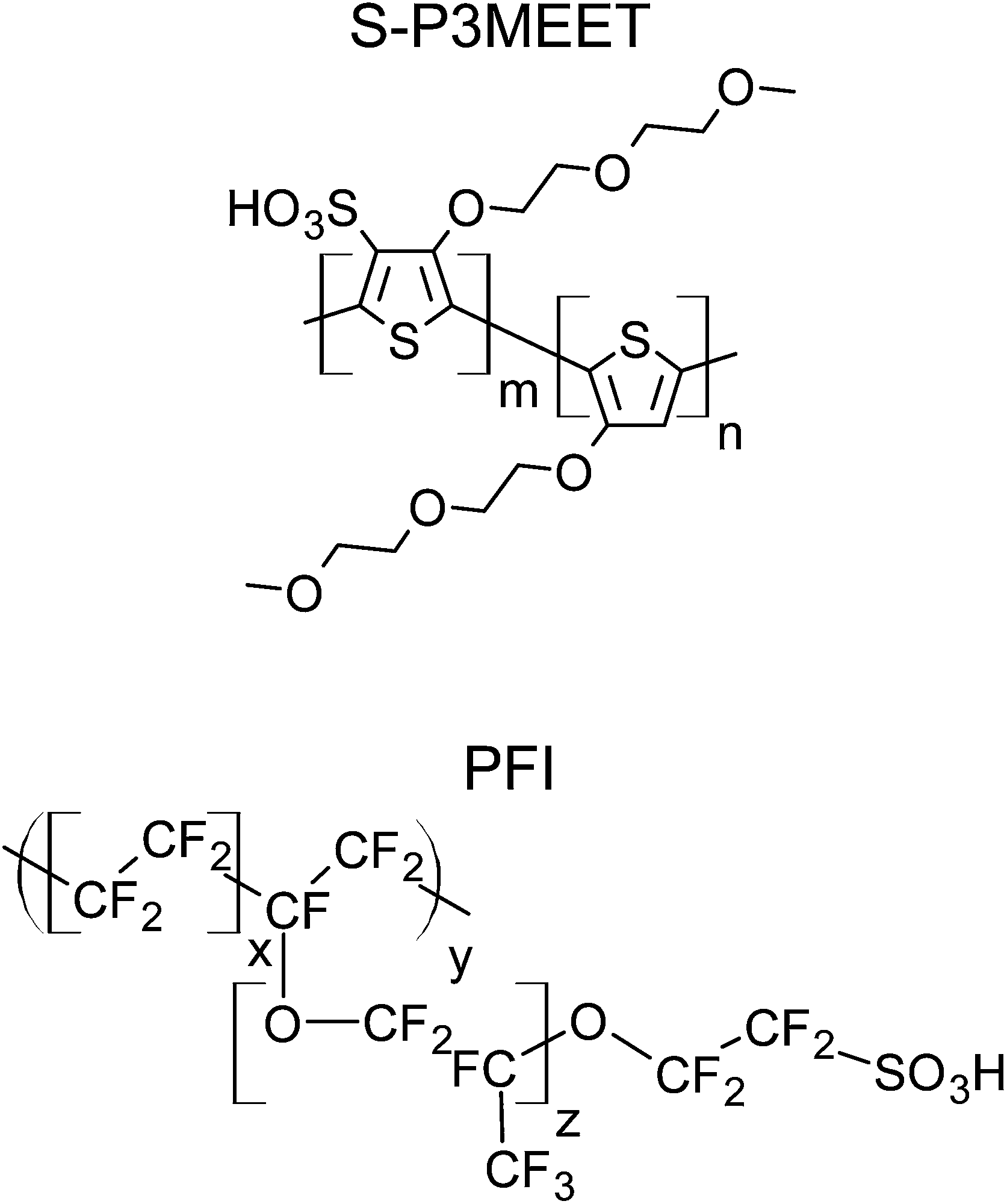 | ||
| Fig. 1 Chemical structures of S-P3MEET (top) and PFI (bottom). | ||
PFI also has the added benefit of having a large Φ. This will allow for tuning of the HTL. A higher Φ HTL may produce more efficient devices when combined with donor polymers with large IP. Steirer et al. showed that in poly(N-9′-heptadecanyl-2,7-carbazole-alt-5,5-(4′,7′-di-2-thienyl-2′,1′,3′-benzodithiol)) (PCDTBT):[6,6]-phenyl-C71 butyric acid methyl ester (PC71BM) devices, a NiOx HTL with Φ = 5.3 eV increased the VOC by 34 mV compared to devices with PEDOT:PSS HTLs.13 This increase was attributed to the increased work function of the NiOx HTL. However, it may be advantageous to have an HTL with Φ that is even higher still. PCDTBT has an IP of −5.27 eV, which matches well with Φ of the NiOx, but there are other polymers with even larger IP like the low band-gap polymer poly[(9,9-dioctylfluorenyl-2,7-diyl)-co-5,5-(4′,7′-di-2-thienyl-2′,1′,3′-benzothiadiazole)] (APFO-3) (IP = 5.8 eV).20 An HTL material with Φ more than 5.3 eV is likely necessary to maximize the efficiency of devices containing polymers with such large IP. PFI has been shown to be successful at creating high Φ HTLs for blue organic light emitting diodes (OLEDs).21–23 Like low band-gap polymers, blue emitting polymers often have a large IP. As an example, for poly(9,9-dioctylfluorene) IP = 5.9 eV.24 Lee et al. showed that adding PFI to the HTL reduced the operating voltage and increased the device luminescent efficiency.21 Adding PFI to the HTL has also been shown to increase device lifetime.25 Similar positive results have also been achieved by spin coating a thin, interfacial layer of PFI on top of the HTL,23 but it is much easier from a processing standpoint to blend PFI with S-P3MEET and reduce the number of fabrication steps.
In this article we successfully use S-P3MEET and PFI create a HTL that mimics the structure of PEDOT:PSS. Using neutron reflectometry (NR), we show that by adding PFI to the S-P3MEET solution we are able to spin coat layers with PFI-enriched top surfaces, and that upon heating to temperatures often experienced in device processing and operation, there is little change in the surface composition. Using the Kelvin probe method, we show that Φ increases with PFI concentration. These measurements also show that heating causes a decrease in Φ. With a combination of near edge X-ray absorption fine structure (NEXAFS) spectroscopy and gas chromatography we find that heating causes PFI to oxidize S-P3MEET. When incorporated into OPV devices with APFO-3:[6,6]-phenyl-C61-butyric acid methyl ester (PCBM) bulk heterojunction active layers, we find that devices with S-P3MEET/PFI HTLs have increased fill factor (FF) and short-circuit current density (JSC) compared to devices with PEDOT:PSS HTLs.
2 Results and discussion
Since one of the reasons for adding PFI to S-P3MEET was to improve energy level alignment with high IP polymers, the first measurement made was of Φ of the PFI-doped S-P3MEET using an ambient Kelvin probe (KP). S-P3MEET was blended with PFI in different ratios ranging from 1–75 weight%. Thin films were obtained by spin coating the blended solutions onto cleaned ITO-coated glass. Additionally, films of pure S-P3MEET and PFI were cast. The films were measured after heating at 110 °C, 120 °C, 150 °C, and 180 °C in air. It was not possible to make measurements of films that had not been heated because films allowed to dry at room temperature dewetted during drying.KP measurements of the pure films showed that heating did not significantly change Φ for S-P3MEET (ΦS) or PFI (ΦP), with ΦS = 5.2 eV and ΦP = 6.2 eV. The measured Φ values for the pure species and blend films are shown in Fig. 2. The value of ΦS is consistent with our previous measurements of S-P3MEET cast from a different solution.19 For the blend films heated at 110 °C, Φ increases with increasing PFI fraction. The increase in Φ is rapid at low concentrations of PFI, but asymptotically approaches ΦP at higher concentrations. The initial rise in Φ can be explained by an increase in the surface concentration of PFI, which has been shown to occur in PEDOT:PSS/PFI blends due to the low surface energy of PFI.21 As the PFI concentration increases, the surface will become predominantly PFI. With heating to 110 °C and 120 °C, the change in work function with increased PFI concentration can be viewed as a change in surface composition between two non-reacting species.
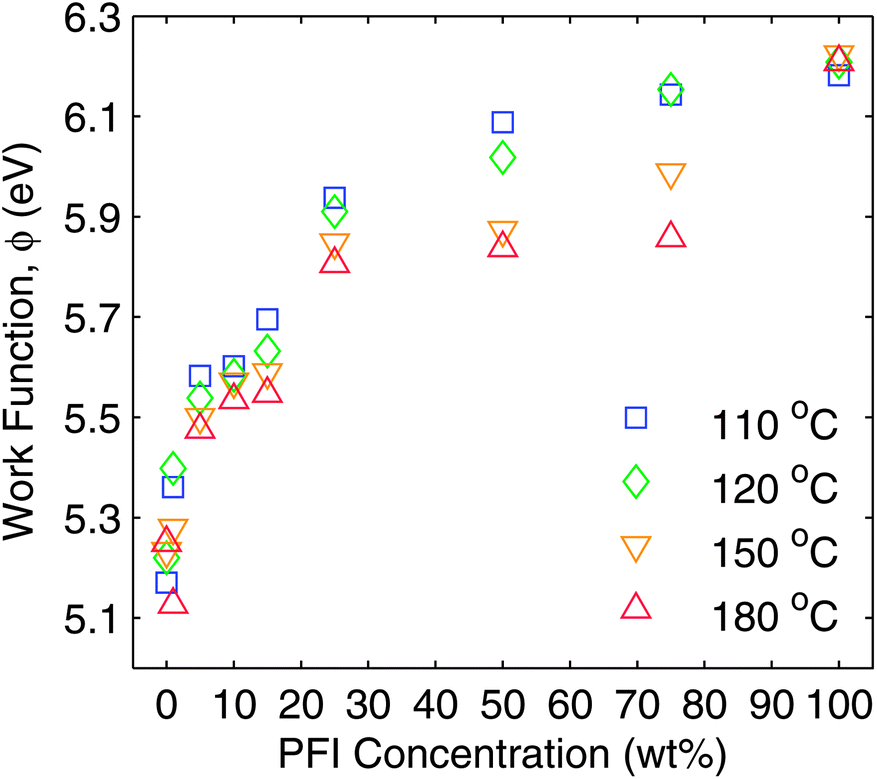 | ||
| Fig. 2 Ambient Kelvin probe measurements of the work function of S-P3MEET, PFI, and S-P3MEET/PFI blend films. Films were measured after heating to 110 °C, 120 °C, 150 °C, and 180 °C for 5 min in air. | ||
When the films were measured after heating at 150 °C and 180 °C for 5 min, there was a noticeable decrease in Φ when compared to the samples heated at 110 °C. This trend is most pronounced for the blend films with higher PFI fractions. For the 75 wt% sample Φ decreases by 0.29 eV, whereas it only decreases by 0.11 eV for the 5 wt% sample. Some concentrations heated to 120 °C also show a decrease in Φ, but there is not a clear trend like there is for the higher annealing temperatures, so we view this as experimental variation. As mentioned above, the pure species do not show the same trend with heating. These changes in Φ indicate that heating is altering the top surface of the film, either physically or chemically. As we will show, both are true, although only chemical changes are responsible for the change in work function.
To determine if a physical (concentration) change is responsible for the change in Φ, we measured blend films using NR. Fluorine has a very different scattering length for neutrons (5.654 fm) than hydrogen (−3.739 fm) in both magnitude and sign.26 Since PFI contains a large number of fluorine atoms, it will have a much higher scattering length density (SLD) than a hydrogen-containing polymer like S-P3MEET, which creates significant contrast. From neat films we determined the SLDs of SP3MEET and PFI to be 2.06 × 10⁻⁶ Å−2 and 3.93 × 10⁻⁶ Å−2, respectively. We measured the neutron reflectivity of films of S-P3MEET with 5 wt% PFI that were coated with a layer of poly(3-hexylthiophene) (P3HT). In our previous work, we showed that surface energy has a strong influence on the vertical distribution of materials in a blend film, and heating samples with an air surface versus a material surface can result in a significantly different vertical materials distribution.27 Therefore, we coated the blend films with P3HT to make the measured sample more similar to an OPV or OLED device, to make comparisons between NR samples and actual devices more believable. For the NR samples, the S-P3MEET/PFI blend film was spin coated on to a silicon wafer and heated at 110 °C for 5 min, followed by deposition of P3HT from chlorobenzene by spin coating. The sample was then measured as-cast and following heating at 120 °C, 150 °C, and 180 °C for 5 min in air. The reflectance as a function of the momentum transfer vector (Q) is shown in Fig. 3a. To determine the distribution of materials, the reflectance data was modeled using a slab model. In a slab model the sample is divided in to several layers, each with their own SLD and thickness. These values along with the ”roughness” of the interface between the layers are used as fit parameters to minimize the χ2 error between the measured and modeled reflectance. The modeled reflectance spectra are shown with the corresponding measured data in Fig. 3a.
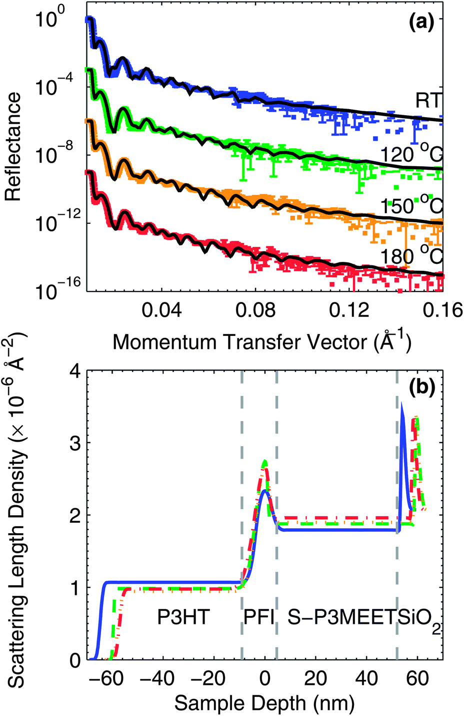 | ||
| Fig. 3 Neutron reflectometry data for S-P3MEET/PFI films coated with P3HT. (a) Reflectance vs. momentum transfer data for the samples heated at RT, 120 °C, 150 °C, and 180 °C after P3HT deposition. The error bars indicate one standard deviation of the measured reflectance value. The modeled reflectance is included for each measurement. (b) SLD profiles generated from the slab model and corresponding to the modeled reflectance data shown in (a). | ||
The SLD profiles determined from the slab models are shown in Fig. 3b. It was determined from the fitting that the most accurate model of the polymer layer stack consisted of three layers (a fourth layer accounted for the native oxide). The profiles have been divided into four sections each corresponding to one of the layers used in the slab model. Starting from the right of Fig. 3b, the first section corresponds to the Si wafer and shows a thin section with higher SLD corresponding to the native oxide of the wafer. The thickness of this oxide layer is thinner than the resolution of the model, but must nevertheless be included to achieve an accurate fit to the data because the SLD of SiO2 is so high. Next, is the bulk of the S-P3MEET/PFI blend layer. Moving further left, on top of the bulk blend layer, is a thin layer with a high SLD. This section of the profile corresponds to the PFI-rich surface layer that forms upon spin coating of the blend layer. The position of the apex was set to 0 nm for easier comparison of the SLD and width of this interfacial layer. Finally, on top of the PFI-rich layer is the layer of P3HT.
All samples, regardless of heating temperature have a prominent PFI-rich layer. This is advantageous for device fabrication because it means that the high PFI concentration will not be significantly affected by heating encountered during subsequent annealing processes or device operation. This result is also positive in regards to device longevity, as it suggests that PFI-rich layer would remain intact over time. With heating to 180 °C, the PFI-rich interlayer gets thinner and the SLD increases, indicating that the layer may be increasing in density and/or purity. The P3HT layers has a higher SLD than we have previously measured for a pure film indicating that some of the PFI is mixing with the P3HT layer during spin coating.28 Interestingly the SLD of the P3HT layer displays a trend that seems correlated with the PFI-rich layer. With increasing temperature, the SLD of the P3HT layer decreases as it is heated to 180 °C, which indicates that the PFI is diffusing out of the P3HT layer, which is consistent with the increase in SLD of the PFI-rich layer. PFI diffusion out of the P3HT layer is a positive result from a device standpoint as excess PFI in the BHJ layer could interfere with the morphology or cause traps, both of which would reduce the performance of OPV devices.
It can also be seen that the SLDs and thickness of the bulk S-P3MEET layer increases with increasing annealing temperature, indicating that with annealing PFI diffuses into S-P3MEET. Though it does not at first appear to be significant, we note that the SLD of the PFI interlayer increases with temperature. Since the concentration of PFI at the surface is not decreasing with temperature, it suggests that a change of the composition at the surface is not responsible for the decrease in Φ with heating. Instead it suggests that an alternative mechanism is responsible for the change in Φ, such as a chemical reaction between PFI and S-P3MEET. Since PFI diffuses out of P3HT, it also suggests no reaction is occurring between the two polymers. We had previously shown that the polymer dopant PSS, with a similar reactive group to PFI, does react with P3HT and does mix with P3HT upon heating. The result shown here suggests that PFI does not follow the same mechanism, or at least has much reduced reactivity with P3HT. We must point out, however, that PSS has a much higher density of reactive groups than PFI. This again shows that the miscibility of aqueous polymers like PSS and non-polar polymers like P3HT can only occur due to an electrochemical reaction. The miscibility between P3HT and PFI is lower than with P3HT and PSS because PFI has fewer reactive sites than PSS, but the doping reaction does still occur with the available sites.
To probe whether a chemical reaction is occurring between S-P3MEET and PFI, we analyzed the sample by NEXAFS because it provides information about element-specific bonding. Additionally, when the spectra are measured in total electron yield (TEY), NEXAFS is a surface specific measurement because only electrons that are within the electron escape depth of a few nm are detected. The S-P3MEET/PFI samples were therefore measured without a P3HT capping layer. This allows us to probe the same region that is measured by the Kelvin probe where the concentration of PFI is the greatest. As discussed above, if the P3HT is present, we also expect a doping reaction with P3HT. Since PFI is a superacid (pKa = −6), it is likely to be more reactive than PSS would be.29
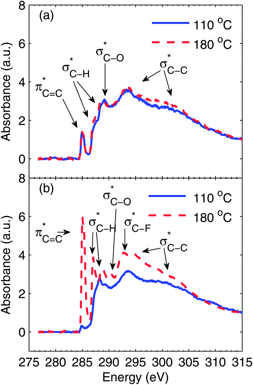
The carbon K-edge NEXAFS spectra for neat S-P3MEET films and blend films containing 1 wt% PFI are shown in Fig. 4. Fig. 4a shows the spectra for neat S-P3MEET films heated at 110 °C and 180 °C. For S-P3MEET, there are several characteristic peaks with some appearing as shoulders that have been assigned as based on the work of Watts et al.30 The first peak at 285.1 eV corresponds to the C1s(C![[double bond, length as m-dash]](https://www.rsc.org/images/entities/char_e001.gif) C) → π*CC transitions of aromatic carbons in the thiophene rings, slightly broadened due to the π*CC–S and π*CC–O bonds. The shoulders around 287.4 eV and 288.4 eV are due to C1s(C–H) → σ*C–H. The peak at 289.2 eV is due to the C1s(C–O) → σ*C–H. The broad features at 293 eV and above are from C1s(C–C) → σ*C–C. The spectra for the two different drying temperatures are quite similar indicating that the chemical structure of S-P3MEET is not changed with heating to 180 °C. This is consistent with the Kelvin probe data, which showed no significant change in ΦS upon heating. The only noticeable change is that C1s(C–H) → σ*C–H peaks have slightly increased in intensity. This indicates a structural rearrangement with more of the side chains at the surface of the film.
C) → π*CC transitions of aromatic carbons in the thiophene rings, slightly broadened due to the π*CC–S and π*CC–O bonds. The shoulders around 287.4 eV and 288.4 eV are due to C1s(C–H) → σ*C–H. The peak at 289.2 eV is due to the C1s(C–O) → σ*C–H. The broad features at 293 eV and above are from C1s(C–C) → σ*C–C. The spectra for the two different drying temperatures are quite similar indicating that the chemical structure of S-P3MEET is not changed with heating to 180 °C. This is consistent with the Kelvin probe data, which showed no significant change in ΦS upon heating. The only noticeable change is that C1s(C–H) → σ*C–H peaks have slightly increased in intensity. This indicates a structural rearrangement with more of the side chains at the surface of the film.
 | ||
| Fig. 4 Near edge X-ray absorption fine structure (NEXAFS) spectra of the carbon K-edge measured in total electron yield (TEY). (a) S-P3MEET films measured after heating at 110 °C and 180 °C. (b) Blend films of S-P3MEET with 1 wt% PFI measured after heating at 110 °C and 180 °C. For both (a) and (b) the spectra are normalized to unity at the energy of 310 eV above the edge. | ||
Fig. 4b shows the spectra for 99![[thin space (1/6-em)]](https://www.rsc.org/images/entities/char_2009.gif) :1 S-P3MEET/PFI sample. Despite the fact that the overall PFI concentration is low, the NR data shows that PFI collects at the surface, so we expect to see an indication that PFI is present in the surface in the NEXAFS spectra. This is exactly what we see. In the spectrum for the S-P3MEET/PFI blend heated to 110 °C the first peak, which is due to aromatic carbon has significantly decreased in intensity. Since PFI contains predominately C–F bonds, its high concentration at the surface will decrease the total amount of aromatic carbon at the surface. We do not see a peak for σ*C–F excitations, which is around 292 eV.31 This is most likely because the peak is small and obscured by the broad σ*C–C at 293 eV.
:1 S-P3MEET/PFI sample. Despite the fact that the overall PFI concentration is low, the NR data shows that PFI collects at the surface, so we expect to see an indication that PFI is present in the surface in the NEXAFS spectra. This is exactly what we see. In the spectrum for the S-P3MEET/PFI blend heated to 110 °C the first peak, which is due to aromatic carbon has significantly decreased in intensity. Since PFI contains predominately C–F bonds, its high concentration at the surface will decrease the total amount of aromatic carbon at the surface. We do not see a peak for σ*C–F excitations, which is around 292 eV.31 This is most likely because the peak is small and obscured by the broad σ*C–C at 293 eV.
Heating the sample at 180 °C results in a significantly different spectrum compared to the sample heated at 110 °C or neat S-P3MEET. The delocalized π peak at 285 eV has significantly increased in intensity. In fact, it is stronger than it was in the undoped samples. The peaks due to the σ*C–H transitions have also increased in intensity, with slight shifts in energy. These changes demonstrate an increased number of empty states in the HOMO of S-P3MEET, meaning that S-P3MEET is being p-doped. This is not surprising as both the sulfonate group and the fluorine atoms of PFI are electron withdrawing. This increase in the density of empty states will cause the ΦS to increase, but will also cause ΦP to decrease. Since the surface is predominately PFI, we observe a decrease in Φ when the blends are heated. There is also the growth of a peak at 292.7 eV, which is likely the σ*C–F peak.31 From NR we know the heating increases the amount of PFI at the top of the HTL. So it is logical that heating causes this peak to become visible.
In our previous work on interfacial doping of P3HT by PEDOT:PSS, we used gas chromatography (GC) to show that P3HT and PSS undergo an electrochemical reaction upon heating, where an electron is donated from P3HT to PSS and is accompanied by the release of H2 gas.28 To determine if a similar reaction has occurred with S-P3MEET and PFI, we performed the identical experiment. The solutions of S-P3MEET and PFI were poured into evaporating dishes and allowed to dry in air for several days. Once dry, the solid polymers were physically mixed together with a mortar and pestle. The mixture was divided and placed into to glass vials which were heated to either 110 °C or 180 °C for 1 h. The gas above the polymer mixture was collected using a syringe and injected into the GC column. The GC traces from the two samples are shown in Fig. 5. Both samples show a peak at approximately 3 min due to atmospheric oxygen, but the sample heated to 180 °C has an additional peak at 2 min. This peak corresponds to H2 gas, indicating that heating to 180 °C results in a chemical reaction. We attribute the production of hydrogen to an electrochemical reaction similar to the one we observed with P3HT and PEDOT:PSS. The sulfonate group of PFI oxidizes S-P3MEET to produce S-P3MEET+ and PFI− in the following mechanism:
 | (1) |
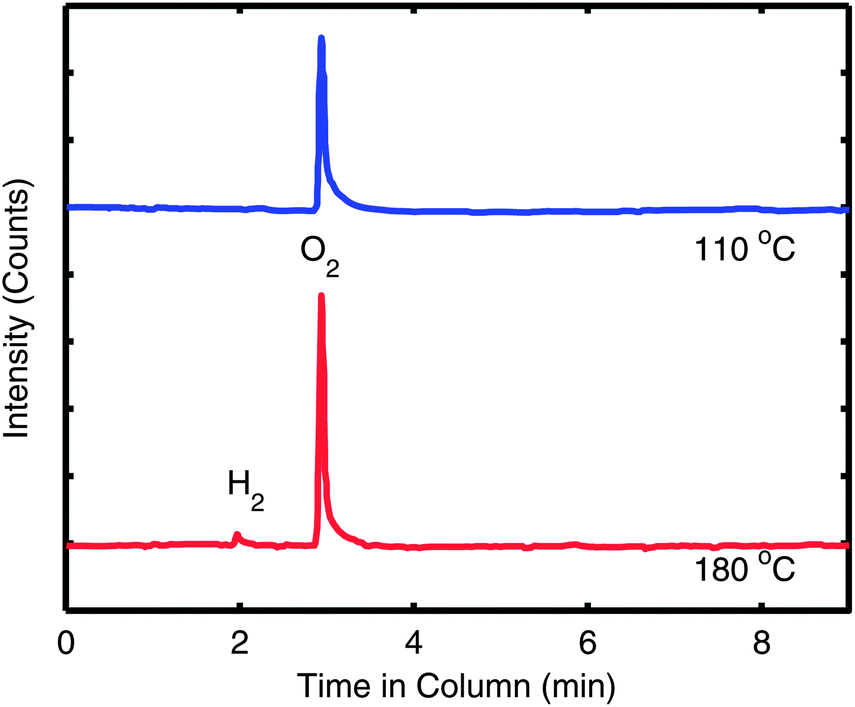 | ||
| Fig. 5 Gas chromatography traces of the gas taken from above S-P3MEET/PFI mixtures which were heated to either 110 °C or 180 °C. The traces are offset for clarity. | ||
This mechanism is sensible as the hydrogen of the PFI sulfonate group is very loosely bound with a pKa of −6. While it could also be possible that the H2 is the result of deprotonation of the sulfonate group of S-P3MEET, density-functional theory calculations of sulfonate groups showed that when they are bound to a hydrocarbon chain, they have a higher ionization potential than when they are bound to a fluorocarbon chain, making deprotonation of S-P3MEET unlikely.22 In addition, no H2 was detected in heated samples of S-P3MEET. This electrochemical reaction is consistent with our NEXAFS data as the S-P3MEET+ will have more empty states in its HOMO level due to oxidation. Since the PFI is in high concentration at the surface, this reaction will mostly occur at the S-P3MEET/PFI interface. These GC data along with the NEXAFS data definitively show that the change in Φ that is observed with heating is due to chemical changes at the S-P3MEET/PFI interface.
Next, we fabricated APFO-3:PCBM (1:4) BHJ OPV devices with S-P3MEET/PFI HTLs. For the HTLs, the spin coating speed was adjusted to achieve 40 nm thick layers for all compositions. The HTLs were heated either at 110 °C or 180 °C prior to spin coating of the active layer and thermal evaporation of the LiF/Al cathode. For the initial current–density/voltage (J–V) measurements, the devices were measured under simulated AM1.5G light without a mismatch correction. A device with a PEDOT:PSS (Clevios P VP 4083) HTL was also fabricated as a control.
The J–V measurements for selected OPV devices with the S-P3MEET/PFI HTL annealed at 110 °C are shown in Fig. 6a and those with the HTL annealed at 180 °C are shown in Fig. 6b. All J–V measurements can be found in Fig. S1 and S2 in the ESI.† The device performance metrics for all of the measured devices, including those shown in Fig. 6, are reported in Table 1. For the pure S-P3MEET HTL devices, VOC is 0.82 V for 110 °C and 0.71 V for 180 °C. The J–V curves for these devices, shown in Fig. 6, exhibit double-diode (“s-kink”) behavior. This is most likely due to the poor energy level alignment between the S-P3MEET and APFO-3.32 In contrast, even though PEDOT:PSS has the same Φ as S-P3MEET, it does not show any double-diode behavior and has a higher VOC of 1.01 V. The difference is likely due to the rather unique nature of PEDOT:PSS. The PSS-rich skin results in unfilled states at the Fermi energy which allows for smaller than expected interfacial barriers with adjacent organic layers.18 However, S-P3MEET has no such skin and thus there is likely a significant extraction barrier due to the mismatch between ΦS and IP of APFO-3, which creates the double-diode shape.
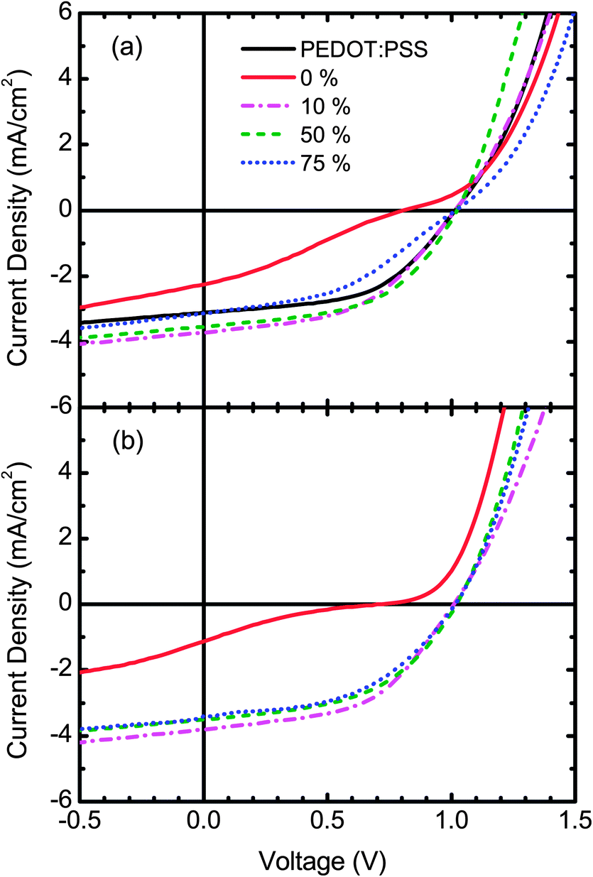 | ||
| Fig. 6 Current–density/voltage measurements of APFO-3:PCBM (1:4) OPV devices with S-P3MEET/PFI HTLs. (a) Measurements of devices where the HTL was heated at 110 °C for 5 min. (b) Measurements of devices where the HTL was heated at 180 °C for 5 min. | ||
| PFI conc. (wt %) | 110 °C | 180 °C | ||||||
|---|---|---|---|---|---|---|---|---|
| V OC (V) | J SC (mA cm−2) | FF | PCE (%) | V OC (V) | J SC (mA cm−2) | FF | PCE (%) | |
| 0 | 0.82 | −2.25 | 0.27 | 0.50 | 0.71 | −1.13 | 0.17 | 0.13 |
| 1 | 1.01 | −3.25 | 0.51 | 1.68 | 0.91 | −2.83 | 0.44 | 1.19 |
| 5 | 1.00 | −3.45 | 0.56 | 1.92 | 0.97 | −3.55 | 0.47 | 1.62 |
| 10 | 1.01 | −3.72 | 0.48 | 1.82 | 1.01 | −3.81 | 0.50 | 1.94 |
| 15 | 1.01 | −3.72 | 0.46 | 1.75 | 1.01 | −3.35 | 0.51 | 1.70 |
| 25 | 1.01 | −3.55 | 0.50 | 1.79 | 1.02 | −3.37 | 0.48 | 1.66 |
| 50 | 1.02 | −3.55 | 0.52 | 1.87 | 1.02 | −3.51 | 0.49 | 1.76 |
| 75 | 1.02 | −3.14 | 0.42 | 1.34 | 1.02 | −3.41 | 0.48 | 1.66 |
| PEDOT:PSS | 1.01 | −3.11 | 0.52 | 1.65 | ||||
When 1 wt% PFI is added to S-P3MEET, there is a marked increase in VOC, just as was the case for the KP measurements of Φ. For the 1 wt% devices, VOC increases to 1.01 V for the 110 °C device, whereas for the 180 °C device it only increases to 0.91 V. Also, the J–V curves no longer show double-diode behavior. The difference in VOC is most likely explained by the observed decrease in Φ with heating. Φ is lower for the sample annealed at 180 °C than at 110 °C resulting in a larger mismatch between Φ and IP, which causes the lower VOC. Unlike the data for Φ at 110 °C which increases with PFI concentration, VOC stays constant for all PFI concentrations. For the samples annealed at 180 °C, VOC stabilizes around 1 V for a PFI concentration of 5 wt% and above. This indicates that energy level of the interface becomes pinned. Since there is a difference between the two temperatures it indicates there is a minimum dopant strength necessary to pin the interface work function. It is also possible that the PFI-rich layer that forms on the top of the S-P3MEET/PFI layer produces a surface dipole that is more important than the energy level alignment. The presence of a surface dipole that lowers interfacial barriers is also consistent with the disappearance of the double diode behavior.
The addition of PFI to the S-P3MEET HTL also increases JSC and FF. The diminished extraction barrier will decrease the series resistance, increasing both JSC and FF. These increases in combination with the increase in VOC result in devices with improved PCE compared to the devices with pure S-P3MEET HTL. For the 110 °C devices the maximum PCE of 1.92% is achieved at a PFI concentration of 5 wt%, whereas for the 180 °C devices the maximum PCE of 1.94% is achieved at 10 wt% PFI. These devices are also over 16% more efficient than the PEDOT:PSS control device. Both HTLs have interfacial layers that are important, but Φ of S-P3MEET/PFI is better matched to the IP of APFO-3 than PEDOT:PSS is.
As the PFI concentration increases the devices with a HTL heated to 110 °C show a decrease in JSC and FF. It can also be seen in Fig. 6 that for the device with 75 wt% PFI the double diode shape is returning. At such high PFI concentrations there is almost certainly no interlayer, as the HTL is mostly PFI. PFI has a very low conductivity at low relative humidity, which is the case for all devices.33 Thus it will be difficult for holes to be extracted from the APFO-3. Also, at high concentrations the PFI will limit the number of conductive percolation pathways in S-P3MEET.
To understand how the conductivity of the S-P3MEET/PFI blends are affected by PFI concentration we measured the in-plane (σ‖) and out-of-plane (σ⊥) conductivities of S-P3MEET/PFI films. The results are shown in Fig. 7. The in-plane measurements in Fig. 7 show a clear trend that conductivity decreases with increasing PFI concentration, starting at 0.11 S cm−1 for pure S-P3MEET and decreasing to 0.008 S cm−1 at 75% PFI. The out-of-plane conductivity remains relatively constant for low PFI concentrations and only decreases 50% over the entire concentration range, which may indicate the formation of a complex microstructure. The microstructure of S-P3MEET/PFI films will be investigated in a future publication.
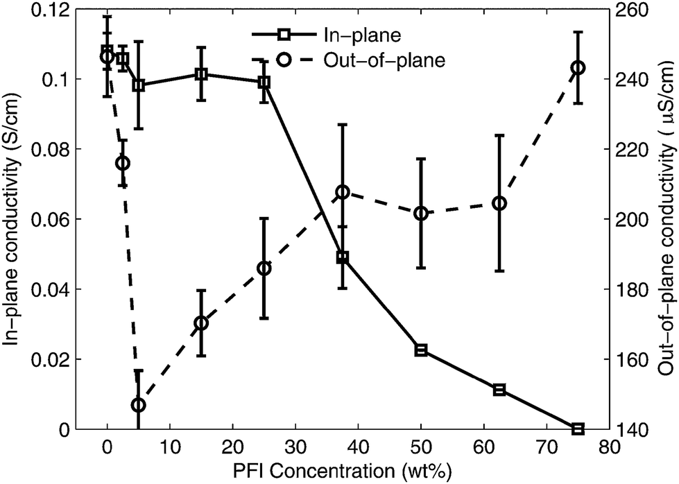 | ||
| Fig. 7 Conductivity measurements of S-P3MEET/PFI films as a function of PFI concentration. The in-plane conductivity was measured by four-wire resistance method. The out-of-plane conductivity was measured between two electrodes. Note the different orders of magnitude of the scales on the vertical axis. Error bars indicate one standard deviation from the mean value. | ||
3 Conclusion
In summary, we show that with the addition of PFI to S-P3MEET we can create a HTL with a materials distribution analogous to PEDOT:PSS. The addition of PFI to S-P3MEET improves device efficiency by decreasing the hole extraction barrier between the HTL and the HOMO of the APFO-3. This work also shows a method to easily tune HTLs for different polymer systems. The thermal stability of the PFI interfacial layer shows that this is a robust system that will not likely be affected by the thermal cycling that PV devices are subjected to under normal operation.4 Experimental
For all measurements and devices, substrates were cleaned in successive ultrasonic baths of acetone, Mucasol detergent (5%), and deionized water. Following the baths they were rinsed with deionized water and dried with nitrogen. All films were deposited by spin coating. Prior to spin coating the substrates were placed in a UV/ozone plasma chamber for 30 min.To make the blend solutions, pure solutions of S-P3MEET (Plexcore OC RG 1110, Plextronics, Inc.) and PFI (Liquion LG-1115, The Nafion Store) were mixed in appropriate ratios to achieve the desired ratio of S-P3MEET to PFI. In order to aid in coating the blends were diluted with a mixture of deionized water (10%), isopropyl alcohol (50%), and 1,3-propanediol (40%). The solutions were stored in air and at room temperature.
Kelvin probe measurements were preformed using an ambient Kelvin probe (KP Technologies, Inc.). The work function of the gold alloy tip was calibrated using a gold surface. Films were deposited onto indium-tin oxide (ITO) coated glass. ITO was exposed by scraping away portions of the films using a knife blade. The samples were electrically connected to the Kelvin prove using conductive metal tape. The samples were heated for 5 min on a hot plate set to 110 °C, 120 °C, 150 °C, or 180 °C.
Neutron reflectometry measurements were performed on the SPEAR flight path at the Lujan Neutron Scattering Center at Los Alamos National Lab.34 Films were spin coated onto 3′′ silicon wafers. First, the S-P3MEET/PFI blend film was deposited. Immediately after spin coating it was annealed at 110 °C for 5 min and then quench-cooled by placing the wafer onto a large metal block. Next a layer of P3HT was deposited by spin coating from a 10 mg mL−1 solution in chlorobenzene. The P3HT solutions was heated at 60 °C for 1 h to ensure complete dissolution. Thickness variations over the entire sample area were less than ±2 nm, as verified with a stylus profilometer. Reflectometry measurements were preformed in air. The sample was measured as cast and after heating in air at 120 °C, 150 °C, and 180 °C for 5 min on a digital hot plate. The measured reflectivity was fit to a slab model, in which the sample film was assumed to consist of a series of n parallel layers, where layer i has a thickness di and constant scattering length density (SLD) ρi, sandwiched between super- (air) and subphases (silicon) of infinite extent. Interlayer “roughness” σi,i+1, which could include contributions from actual roughness between layers or from interlayer mixing, was accounted for by an error function SLD profile centered at the interface connecting the SLDs of the adjacent layers i and (i + 1). Slab model fitting to the measured data were carried out using MOTOFIT.35 The SLDs of air and silicon were taken to be ρair = 0 and ρSi = 2.07 × 10⁻⁶ Å−2, respectively.26 For pure P3HT, ρP3HT = 0.786 × 10⁻⁶ Å−2, which was determined in previous measurements.28
Near edge X-ray absorption fine structure measurements on the carbon K-edge were performed on Beamline 6.3.1 at the Advanced Light Source at Lawrence Berkeley National Laboratory. Samples were prepared by spin coating the solutions on to ITO-coated glass. The samples were heated at either 110 °C or 180° in air for 5 min. The spectra were taken with a Galileo 4716 channeltron electron multiplier. The TEY signal was normalized by the incident beam intensity I0, a linear background and a small pre-edge feature due to carbon contamination of the beam line were subtracted, and the spectra were normalized to unity above the edge at 315 eV. The energy was calibrated by setting the strong resonance peak corresponding to excitation into the π* CC orbital to 285.13 eV.30 Repeat scans over the same spot indicated no signs of radiation damage in any of the samples.
For the gas chromatography measurements the solutions of S-P3MEET and PFI were dried in evaporating dishes until completely dry. Equal masses of S-P3MEET and PFI were mechanically mixed using an agate mortar and pestle. The solid mixture was divided amongst two glass vials and filled with silica beads to decrease the total gas volume in the vials. The vials were sealed with Al-coated silicone septums. The sealed vials were heated for 1 h at either 110° or 180°. For the GC measurement, 100 μL of the vapor in the vials was drawn into a syringe and injected in to a Varian 3800 gas chromatograph equipped with a TCD detector. The injector temperature was 250°. The column temperature was 35° with a nitrogen pressure of 80 psi and a flow rate of 4 mL min−1.
Photovoltaic devices were fabricated on patterned ITO-coated glass in a conventional architecture. Blends of S-P3MEET and Nafion were spin coated onto the ITO glass in air and annealed directly thereafter. The active layer was bulk heterojunction blend of poly[(9,9-dioctylfluorenyl-2,7-diyl)-co-5,5-(4′,7′-di-2-thienyl-2′,1′,3′-benzothiadiazole)] (APFO-3) and [6,6]-phenyl-C61-butyric acid methyl ester (PCBM). APFO-3 and PCBM were individually dissolved in chlorobenzene at concentrations of 12 and 24 mg mL−1, respectively. The solutions were heated at 50 °C overnight to ensure dissolution of the solids. The two solutions were blended so that the ratio of PCBM to APFO-3 was 4:1. The active layer was spin coated in a N2 glove box. Following deposition of the active layer the samples were transferred to a vacuum chamber, where the cathode metal was deposited by thermal evaporation. 0.7–1.0 nm of Ca was deposited at a rate of at 0.2 Å s−1, which was then covered with 60 nm of Al that was deposited at 1.5 Å s−1. Current voltage measurements were made under 1 Sun of simulated AM1.5G light (Radiant Source Technologies) with no mismatch correction. The intensity of the simulator was calibrated using a certified Si reference cell (VLSI Standards, Inc.). The devices were measured with an as-cast bulk heterojunction.
For in-plane conductivity measurements the slides were scored using a steel cutting wheel to divide the glass into nine (0.33 × 0.33 in2) subsections. Following light rinsing with acetone, Mucasol, and deionized water, the substrates were transferred to a high vacuum chamber (MBraun). Four electrodes (1 × 5 mm2, 1 mm spacing) composed of 5 nm of chromium followed by 95 nm of gold were deposited by thermal evaporation. Following electrode deposition the samples were rinsed again and cleaned in the UV/ozone plasma. For out-of-plane measurements, 5 nm of Cr followed by 95 nm of Au was deposited onto ITO-coated glass. After electrode deposition, the substrates were lightly rinsed and UV/ozone cleaned. Films were of the S-P3MEET/PFI blends were then spin coated onto the substrates (for both geometries). The out-of-plane samples were returned to the high vacuum chamber and 100 nm of gold was deposited through the same mask as was used for the in-plane samples to give an active area of 0.05 cm2. Electrical measurements were performed with a Keithely 2420 source measurement unit.
Acknowledgements
This work and S.A.M. were supported by the US Department of Energy EERE Solar America Initiative under Contract no. DE-FG3608GO18018. This work benefited from the use of the Lujan Neutron Scattering Center at LANSCE funded by the DOE Office of Basic Energy Sciences and Los Alamos National Laboratory under DOE Contract DE-AC52-06NA25396 and we thank Jarek Majewski and Peng Wang for their assistance with measurements and data analysis. Part of this work was performed under the auspices of the U.S. Department of Energy by Lawrence Livermore National Laboratory under Contract DE-AC52-07NA27344. We would also like to thank Plextronics for the donation of S-P3MEET and Jonas Bergqvist and the research group of Prof. Mats Andersson for providing the APFO-3 polymer. We thank Elke Arenholz for help with the NEXAFS measurements. L.A.B. is a Alfred P. Sloan Foundation Fellow.References
- F. C. Krebs, T. D. Nielsen, J. Fyenbo, M. Wadstrom and M. S. Pedersen, Energy Environ. Sci., 2010, 3, 512 CAS.
- Heliatek, Heliatek consolidates its technology leadership by establishing a new world record for organic solar technology with a cell efficiency of 12%, 2013, http://www.heliatek.com/wpcontent/uploads/2013/01/<?ccdc_no 130116?>130116<?ccdc END?>%<?pdb_no 20PR?>20PR<?pdb END?>%20Heliatek_achieves_record_cell_effiency_for_OPV.pdf Search PubMed.
- M. Svensson, F. L. Zhang, S. C. Veenstra, W. J. H. Verhees, J. C. Hummelen, J. M. Kroon, O. Inganäs and M. R. Andersson, Adv. Mater., 2003, 15, 988 CrossRef CAS.
- D. Muhlbacher, M. Scharber, M. Morana, Z. G. Zhu, D. Waller, R. Gaudiana and C. Brabec, Adv. Mater., 2006, 18, 2931 CrossRef.
- H. Y. Chen, J. H. Hou, S. Q. Zhang, Y. Y. Liang, G. W. Yang, Y. Yang, L. P. Yu, Y. Wu and G. Li, Nat. Photonics, 2009, 3, 649–653 CrossRef CAS.
- N. Blouin, A. Michaud, D. Gendron, S. Wakim, E. Blair, R. Neagu-Plesu, M. Belletête, G. Durocher, Y. Tao and M. Leclerc, J. Am. Chem. Soc., 2008, 130, 732–742 CrossRef CAS PubMed.
- E. Wang, L. Hou, Z. Wang, S. Hellström, F. Zhang, O. Inganäs and M. R. Andersson, Adv. Mater., 2010, 22, 5240–5244 CrossRef CAS PubMed.
- S. E. Shaheen, C. J. Brabec, N. S. Sariciftci, F. Padinger, T. Fromherz and J. C. Hummelen, Appl. Phys. Lett., 2001, 78, 841–843 CrossRef CAS.
- F. Zhang, M. Cedar and O. Inganäs, Adv. Mater., 2007, 19, 1835 CrossRef CAS.
- J. Luo, H. Wu, C. He, A. Li, W. Yang and Y. Cao, Appl. Phys. Lett., 2009, 95, 043301 CrossRef.
- Z. Tang, L. M. Andersson, Z. George, K. Vandewal, K. Tvingstedt, P. Heriksson, R. Kroon, M. R. Andersson and O. Inganäs, Adv. Mater., 2012, 24, 554–558 CrossRef CAS PubMed.
- C. H. Hsieh, Y. J. Cheng, P. J. Li, C. H. Chen, M. Dubosc, R. M. Liang and C. S. Hsu, J. Am. Chem. Soc., 2010, 132, 4887–4893 CrossRef CAS PubMed.
- K. X. Steirer, P. F. Ndione, N. E. Widjonarko, M. T. Lloyd, J. Meyer, E. L. Ratcliff, A. Kahn, N. R. Armstrong, C. J. Curtis, D. S. Ginley, J. J. Berry and D. C. Olson, Adv. Energy Mater., 2011, 1, 813–820 CrossRef CAS.
- V. Shrotriya, G. Li, Y. Yao, C. W. Chu and Y. Yang, Appl. Phys. Lett., 2006, 88, 073508 CrossRef.
- M. D. Irwin, B. Buchholz, A. W. Hains, R. P. H. Chang and T. J. Marks, Proc. Natl. Acad. Sci. U. S. A., 2008, 105, 2783–2787 CrossRef CAS.
- K. X. Steirer, J. P. Chesin, N. E. Widjonarko, J. J. Berry, A. Miedaner, D. S. Ginley and D. C. Olson, Org. Electron., 2010, 11, 1414–1418 CrossRef CAS PubMed.
- S. A. Mauger, L. Chang, C. Rochester and A. J. Moulé, Org. Electron., 2012, 13, 2747 CrossRef CAS PubMed.
- J. Hwang, F. Amy and A. Kahn, Org. Electron., 2006, 7, 387–396 CrossRef CAS PubMed.
- S. A. Mauger and A. J. Moulé, Org. Electron., 2011, 12, 1948–1956 CrossRef CAS PubMed.
- L. Andersson and O. Inganäs, Appl. Phys. Lett., 2006, 88, 082103 CrossRef.
- T.-W. Lee, O. Kwon, M.-G. Kim, S. Park, J. Chung, S. Kim, Y. Chung, J.-Y. Park, E. Han, D. Huh, J.-J. Park and L. Pu, Appl. Phys. Lett., 2005, 87, 231106 CrossRef.
- T.-W. Lee, Y. Chung, O. Kwon and J.-J. Park, Adv. Funct. Mater., 2007, 17, 390–396 CrossRef CAS.
- B. Chin, Y. Choi, H.-I. Baek and C. Lee, Proc. SPIE, 2009, 7415, 741510 CrossRef PubMed.
- S. Janietz, D. D. C. Bradley, M. Grell, C. Giebeler, M. Inbasekaran and E. Woo, Appl. Phys. Lett., 1998, 73, 2453 CrossRef CAS.
- J. S. Huang, G. Li and Y. Yang, Appl. Phys. Lett., 2005, 87, 112105 CrossRef.
- National Institute of Standards and Technology (NIST) Center for Neutron Research, Scattering Length Density Calculator: http://www.ncnr.nist.gov/resources/sldcalc.html.
- S. A. Mauger, L. Chang, S. Friedrich, C. W. Rochester, D. M. Huang, P. Wang and A. J. Moulé, Adv. Funct. Mater., 2013, 23(15), 1935–1946 CrossRef CAS.
- D. M. Huang, S. A. Mauger, S. Friedrich, S. J. George, D. Dumitriu-LaGrange, S. Yoon and A. J. Moulé, Adv. Funct. Mater., 2011, 21, 1657–1665 CrossRef CAS.
- J. Serpico, S. Ehrenberg, J. Fontanella, X. Jiao, D. Perahia, K. McGrady, E. Sanders, G. Kellogg and G. Wnek, Macromolecules, 2002, 35, 5916–5921 CrossRef CAS.
- B. Watts, S. Swaraj, D. Nordlund, J. Lüning and H. Ade, J. Chem. Phys., 2011, 134, 024702 CrossRef CAS PubMed.
- D. Schmeisser, M. Tallarida, K. Henkel, K. Müller, D. Mandal, D. Chumakov and E. Zschech, Mater. Sci.-Pol., 2009, 27, 141–157 CAS.
- W. Tress, K. Leo and M. Riede, Adv. Funct. Mater., 2011, 21, 2140–2149 CrossRef CAS.
- R. Paul and S. J. Paddison, J. Chem. Phys., 2001, 115, 7762–7771 CrossRef CAS.
- M. Dubey, M. S. Jablin, P. Wang, M. Mocko and J. Majewski, Eur. Phys. J. Plus, 2011, 126, 110 CrossRef.
- A. Nelson, J. Appl. Crystallogr., 2006, 39, 273–276 CrossRef CAS.
Footnotes |
| † Electronic supplementary information (ESI) available. See DOI: 10.1039/c3tc30973h |
| ‡ Current address: Process Technology and Advanced Concepts Group, National Renewable Energy Laboratory, Golden, CO 80401, USA. |
| This journal is © The Royal Society of Chemistry 2014 |