A simple approach to the fabrication of fluorine-doped zinc oxide thin films by atomic layer deposition at low temperatures and an investigation into the growth mode†
Received
29th July 2013
, Accepted 19th October 2013
First published on 23rd October 2013
Abstract
A simple low-temperature fabrication of fluorine-doped ZnO (ZnO:F) thin films by atomic layer deposition (ALD) was investigated and the growth mode of the films was analyzed. A novel method for fluorine doping into a ZnO matrix was successfully developed that uses ALD with a home-made fluorine source at a low deposition temperature of 140 °C, which is low enough for films to be applied to a plastic substrate. The fluorine doping concentration was controlled from 0 at.% to 1.2 at.% by manipulating the pulse sequence ratio of the oxygen source (deionized water) and the home-made fluorine source. Structural and morphological properties were investigated by X-ray diffraction and field emission scanning electron microscopy. The growth mode of the films was studied by grazing-incidence wide-angle X-ray diffraction. The grain growth orientation was found to change significantly as the fluorine concentration was increased due to the characteristics of fluorine doping in the oxygen sites of ZnO. This phenomenon could be explained by a perturbation and passivation effect resulting from the fluorine doping mechanism, with the fluorine anions filling oxygen-related defect sites in the ZnO lattice. A photoluminescence study confirmed the diminishment of defect sites and showed that, due to the Burstein–Moss effect, the optical transmittance in the visible region increased significantly with an increase in the fluorine doping concentration from 80.87% to 83.02%. The lowest resistivity was 1.876 × 10⁻³ Ω cm for ZnO thin films doped with 1.0 at.% fluorine when the carrier concentration and mobility were 1.375 × 1020 cm−3 and 24.20 cm2 V−1 s−1, respectively.
1 Introduction
Transparent conducting oxides (TCOs) are oxide semiconductors that are transparent in the visible region and offer broad controllability of electrical conductivity. The combination of optical transparency with electrical conductivity of TCOs allows for transparent electrodes of next-generation optoelectronic applications in flat-panel displays (FPDs),1 photovoltaic (PV) devices,2 and organic light-emitting diodes (OLEDs).3 Moreover, in response to the additional requirements of optoelectronic applications, TCO layers can be deposited on flexible, light-weight, and small plastic substrates at a temperature under the glass transition temperature of plastic substrates. Tin-doped indium oxide (indium tin oxide; ITO) has been the material most widely used for transparent electrodes for optoelectronic devices because of its excellent transparency in the visible region and its high electrical conductivity. However, due to a number of problems regarding the use of ITO, such as environmental pollution, high costs due to the rarity of indium, the need for expensive deposition techniques, and the instability of indium in hydrogen plasma, it is necessary to identify indium-free TCO materials. Zinc oxide (ZnO), which is an n-type, direct, wide band gap (3.3 eV) semiconductor with a high exciton binding energy (60 meV), has been actively explored as a promising indium-free TCO material. Intrinsic ZnO, however, has a lower electron concentration, 1018 to 1019 cm−3, (electrons via Zn interstitials and/or O vacancies) compared to ITO (∼1021 cm−3). Therefore, ZnO requires doping with either trivalent metal cations (Group III elements; Al, Ga, B)4–6 or halogen anions (Group VII elements; F, Cl)7,8 to yield degenerately doped semiconductors with a high electron concentration (up to 1021 cm−3) while maintaining high electron mobility.
Among recent investigations of suitable dopants for ZnO, most have used impurity-doped ZnO TCO films with metallic cation dopants, while there have been comparatively few studies on the TCO characteristics of ZnO doped with halogen anions. Nevertheless, the most effective dopant for ZnO matrices is F. In F-doped ZnO (ZnO:F) films, as compared with metallic-cation-doped ZnO films, electronic perturbation is largely confined to the filled valence band when F is substituted for O, and the scattering of conduction electrons is reduced, which leads to the low resistivity combined with high mobility of ZnO:F films.7 F ions are also about the same size as O ions (F−: 1.31 Å and O2−: 1.38 Å), and thus F would be predicted to act as an n-type dopant and to maintain the highest electron mobility in ZnO without lattice distortions.9 Other advantages of ZnO:F films include the reduction of the known number of Os2−/Os− surface states and an increase in carrier mobility,10 resulting in a higher doping efficiency of the F dopant than that of a metallic cation dopant in ZnO for the optimization of electrical conductivity.11 However, in spite of these merits, only very few studies on ZnO:F thin films have been conducted because it is very difficult to incorporate F into the ZnO matrix.
Even though doping with F in ZnO films is difficult, the fabrication of ZnO:F films has been attempted using several effective deposition techniques including chemical spray pyrolysis,12 chemical vapor deposition (CVD),7 electron beam evaporation,10 pulsed laser deposition,13 and radio frequency (rf) magnetron sputtering.14 Most investigations into ZnO:F films use a fabrication method relying on solution-based spray pyrolysis, and the resulting resistivity values have ranged from 10−1 to 10−2 Ω cm. The chemical spray method allows for the relatively easy fabrication of ZnO:F films, but the electrical enhancement of ZnO:F films using this method has been far from satisfactory. There have been other notable reports on ZnO:F films fabricated using CVD and electron beam evaporation.7,10 Resistivity values are as low as 4 × 10⁻⁴ and 7.95 × 10⁻⁴ Ω cm and mobilities are as high as 40 and 46.2 cm2 V−1 s−1 in the reports of Hu et al. and Xu et al., respectively. In spite of the low resistivity and high mobility of the ZnO:F films deposited by the aforementioned techniques, the growth temperature was over 450 °C, and additional post-annealing or oxidization was necessary.
The atomic layer deposition (ALD) technique is a very advanced deposition method for low temperature-processing that yields highly uniform films. The ALD technique is a thin film growth method employing self-limiting surface chemistry comprising repeating processes of pulses and purges with precursors in which the source materials are kept separate during the entire deposition process. Therefore, ALD allows for low-temperature growth, better step coverage (high aspect ratio), and good uniformity, along with the ability to control the film thickness through a number of ALD cycles. Moreover, the separate dosing of the precursors prevents gas phase reactions, which permits the use of highly reactive precursors and provides sufficient time for each reaction step to reach completion. These excellent properties allow for the deposition of electronic devices with complex 3D structures and for processing at relatively low temperatures, facilitating the use of flexible substrates. However, ZnO:F thin films have not been investigated using ALD due to the absence of an F-related metal–organic source. There have been a few reports regarding the fabrication of metal fluorides such as CaF2 (ref. 15) and MgF2 (ref. 16) by using TiF4 and TaF5 sources as an F source, respectively. However, those sources are not suitable for the deposition of ZnO:F films due to the high levels of metal impurity of Ti or Ta in ZnO. With ALD-TCO, Al-doped ZnO (ZnO:Al) films should be fabricated as alloys of ZnO layers and Al2O3 layers with a laminated structure, while a laminated structure was not necessary to fabricate ZnO:F films in this work. Therefore, ALD-ZnO:Al films should be grown at a relatively high temperature of over 200 °C for satisfactory dopant activation in order to improve the electrical conductivity.4
Thus, in this study, home-made F sources were fabricated by mixing 50 mL of deionized water (DI water) and 0.5 mL of dilute hydrogen fluoride (HF 48–51% diluted in water). In turn, F was successfully doped into the ZnO matrix by ALD at a low growth temperature of 140 °C. An analysis of the F doping mechanism in the ALD-ZnO films and a quantitative analysis of the doping concentration in the ZnO matrix were performed. The electrical, structural, morphological, and optical characteristics of the ZnO:F films were examined as a function of doping concentration.
2 Experimental section
2.1 Novel atomic layer deposition of F-doped ZnO thin films
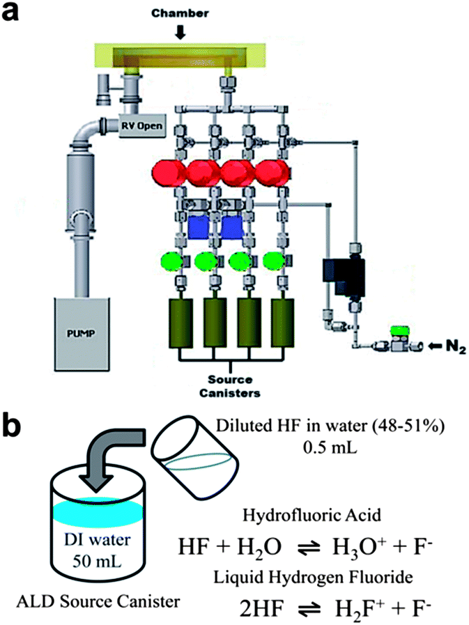
Undoped ZnO and ZnO:F thin films were deposited on thermally oxidized SiO2 (100 nm) on Si substrates, Si substrates, and LCD glass (Fusion 1737) substrates via ALD using a traveling wave type Lucida D100 system (NCD Technology, Inc. Korea) at a deposition temperature of 140 °C and a working pressure of less than 1 Torr. A schematic of the ALD equipment is shown in Fig. 1a. Diethylzinc (DEZ, Hansol Chemical Co., Ltd., Korea) and deionized water (DI water) were used as a precursor for the Zn and O reactant, respectively. A home-made F source was created by mixing 50 mL DI water and 0.5 mL diluted hydrogen fluoride (HF 48–51% diluted in water). This solution was stirred for 5 min in order to uniformly disperse the HF in DI water before the solution was charged to a canister. The chemical state of this source solution is composed of hydrofluoric acid and/or liquid hydrogen fluoride (Fig. 1b). DEZ was kept below 10 °C by using a chiller and delivered into a chamber with a high purity N2 (99.999%) carrier gas flow of 20 sccm (standard cubic centimeters per minute). ALD growth cycles for undoped ZnO thin films were as follows: DEZ pulse (0.1 s) → N2 purge (10 s) → H2O pulse (0.1 s) → N2 purge (10 s) (Fig. 2a). In order to incorporate the desired F doping content into ZnO thin films, water (H2O) and the home-made F source (H2O/HF) were alternately pulsed with a controlled x![[thin space (1/6-em)]](https://www.rsc.org/images/entities/char_2009.gif) :y ratio. For example, for Zn-O:Zn-O/F (4:1) samples, one super cycle comprised four (x = 4) repeats of the ALD sequence, DEZ (0.1 s) pulse → N2 purge (10 s) → H2O pulse (0.1 s) → N2 purge (10 s) and one (y = 1) ALD sequence, DEZ (0.1 s) pulse → N2 purge (10 s) → H2O/HF pulse (0.1 s) → N2 purge (10 s) (Fig. 2b). The sequence of the ALD-ZnO:F films with single reactant (H2O/HF) was DEZ pulse (0.1 s) → N2 purge (10 s) → H2O/HF pulse (0.1 s) → N2 purge (10 s), and the F concentration could be maximized from this ALD sequence (Fig. 2c).
:y ratio. For example, for Zn-O:Zn-O/F (4:1) samples, one super cycle comprised four (x = 4) repeats of the ALD sequence, DEZ (0.1 s) pulse → N2 purge (10 s) → H2O pulse (0.1 s) → N2 purge (10 s) and one (y = 1) ALD sequence, DEZ (0.1 s) pulse → N2 purge (10 s) → H2O/HF pulse (0.1 s) → N2 purge (10 s) (Fig. 2b). The sequence of the ALD-ZnO:F films with single reactant (H2O/HF) was DEZ pulse (0.1 s) → N2 purge (10 s) → H2O/HF pulse (0.1 s) → N2 purge (10 s), and the F concentration could be maximized from this ALD sequence (Fig. 2c).
 |
| | Fig. 1 Schematic diagram of (a) the atomic layer deposition system. (b) Illustration of the fabrication method for the home-made fluorine source and the predicted chemical state of the fluorine source solution. | |
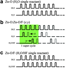 |
| | Fig. 2 Schematic diagram of the process sequence used to grow (a) undoped and (b and c) fluorine-doped ZnO thin films. O/F indicates the fluorine single source of mixed H2O and diluted HF (48–51% in H2O). In (b), x is the pulse ratio of the H2O source and y is the pulse ratio of the fluorine source (H2O/HF) in one super cycle. The source pulse time and high purity N2 purge time were fixed at 0.1 and 10 s, respectively. | |
2.2 Extrinsic F doping in ZnO via ALD
Undoped ZnO thin films were fabricated using the ALD process sequence (Fig. 2a). The general ALD reaction for the fabrication of ZnO films is very simple and has been reported previously.17,18 The overall reaction during the formation of ZnO films can be generally defined by formulas (1) and (2):| | | ZnOH* + Zn(C2H5)2 → ZnOZnC2H5* + C2H6 [DEZ pulse] | (1) |
| | | ZnOZnC2H5* + H2O → ZnOZnOH* + C2H6 [H2O pulse] | (2) |
where asterisks denote the chemical species on the film surface. By the repetition of reactions (1) and (2), undoped ZnO films can be deposited with atomic layer control on various substrates. The general overall reaction schemes for ZnO:F films (Fig. 2b and c) are given as follows:| | | ZnOH* + Zn(C2H5)2 → ZnOZnC2H5* + C2H6 [DEZ pulse] | (3) |
| | | ZnOZnC2H5* + H2O + HF → ZnOZnOH* + HF + C2H6 [H2O/HF pulse] | (4) |
| | | ZnOZnC2H5* + HF → ZnOZnF + C2H6 [F doping in ZnO matrix] | (5) |
when DEZ and H2O/HF were pulsed, ZnO and ZnO:F layers are formed simultaneously by reactions (3), (4), and (5). Thus, it is clearly the F doping step that supplies the F doping source through the injection sequence of H2O/HF.
Table 1 includes detailed information regarding experimental parameters such as the sample I.D., DEZ-H2O (Zn-O):DEZ-H2O/HF (Zn-O/F) cycle ratio, growth temperature, film thicknesses after a total of 1200 process cycles, growth rates, HF pulse portion in one super cycle, and the atomic content of Zn, O, and F in the films as obtained by energy dispersive X-ray analysis (EDX). The doping concentration of F in the ZnO films could be controlled by the number of F source injection times, as demonstrated in Fig. 2.
Table 1 Sample identification (I.D.), DEZ–H2O (Zn-O):DEZ–H2O/HF (Zn-O/F) cycle ratio, growth temperature, film thicknesses after a total of 1200 process cycles as measured by ellipsometry, growth rates, HF pulse portion in one super cycle, and the atomic content of Zn, O, and F in the films as obtained by EDX
| Sample I.D. |
Cycle ratio (Zn-O:Zn-O/F) |
Growth temp. (°C) |
t (nm) |
Growth rate (Å per cycle) |
HF pulse portion in 1 super cycle (%) |
EDX results (at.%) |
| Zn |
O |
F |
|
In the case of ZnO:F{0.2}, the F-concentration was estimated by a linear plot (Fig. 3b).
|
| ZnO |
1:0 |
140 |
260 ± 5 |
2.165 |
0 |
50.7 ± 0.1 |
49.3 ± 0.1 |
0 |
| ZnO:F{0.2}a |
4:1 |
262 ± 5 |
2.180 |
0.10 |
51.3 ± 0.1 |
48.7 ± 0.1 |
Not detected |
| ZnO:F(0.5) |
1:1 |
281 ± 5 |
2.343 |
0.25 |
51.3 ± 0.1 |
48.2 ± 0.1 |
0.5 ± 0.1 |
| ZnO:F(0.7) |
1:2 |
281 ± 5 |
2.343 |
0.34 |
51.2 ± 0.1 |
48.1 ± 0.1 |
0.7 ± 0.1 |
| ZnO:F(1.0) |
1:4 |
287 ± 5 |
2.390 |
0.40 |
51.4 ± 0.1 |
47.6 ± 0.1 |
1.0 ± 0.1 |
| ZnO:F(1.2) |
0:1 |
301 ± 5 |
2.510 |
0.50 |
51.1 ± 0.1 |
47.7 ± 0.1 |
1.2 ± 0.1 |
2.3 The analysis of the properties of ZnO and ZnO:F thin films
The electrical performance, including the resistivity (ρ) and Hall coefficient (RH) parameters, was obtained by the van der Pauw method at room temperature using a Hall effect measurement system (Ecopia HMS3000) without the use of metal soldering for the electrical contacts due to high film quality (DC current = 10 mA) in the magnetic field up to 0.57 T. The film thicknesses were determined by ellipsometry and confirmed by cross-sectional field emission scanning electron microscopy (FE-SEM; JEOL, JSM 7001F) of the cleaved samples (Fig. S1, ESI†). X-ray diffraction analysis used (XRD; Rigaku Ultima IV) Cu Kα radiation (λ = 1.5418 Å). For surface morphology analysis, FE-SEM was employed, and quantitative elemental analysis was conducted using EDX with 15 kV energy, 300 s integration time, and 35° take-off angle (JEOL, JSM 7001F attached with OXFORD X-MaxN EDX detector (Analysis software was AZtecEnergy of OXFORD instruments.)). The surface elemental analysis of the films was carried out by using X-ray photoelectron spectroscopy (XPS; Thermo VG, UK) with monochromated Al X-ray sources (Al kα line: 1486.6 eV) and an X-ray power of 12 kV and 3 mA. Room-temperature photoluminescence (PL) spectroscopy (Hitachi P7000) was conducted, and optical transmittance spectra were monitored using an ultraviolet-visible-near infrared (UV-vis-NIR) spectrophotometer (V-570, JASCO) in the range of 200 to 2500 nm. Grazing-incident wide-angle X-ray diffraction (GIWAXD) used the 9A beam line at the Pohang Light Source (PLS, Korea), and photoemission spectroscopy (PES) used the 8A2 beam line at PLS. Au foil was used as the reference material for the calibration of the kinetic energy shift.
3 Results and discussion
3.1 Fluorine concentration and ALD-growth rate
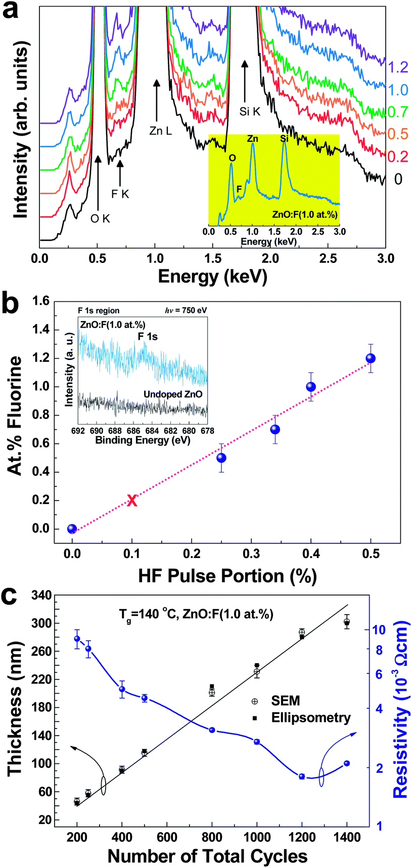
The EDX spectra of undoped ZnO and ZnO:F thin films with various F contents deposited on Si substrates are shown in Fig. 3a. The intensity of the F signal (peaks at 0.68 keV) was clearly enhanced with an increase in the home-made F source pulse ratio. The inset of Fig. 3a is the EDX result of ZnO:F(1.0) films (the representative samples in this work) in the logarithmic scale. The plot of the concentration of F in the ZnO matrix as a function of HF pulse portion as measured by EDX is shown in Fig. 3b. The HF pulse portion in one super cycle could be evaluated by the content of HF in the diluted F source solution (0.5 mL of 48–51% diluted HF in 50 mL water, about 0.5% HF in the source canister) using an HF pulse portion (%) = [y/(x + y)] × 0.5%. The atomic concentration of F in the films increased linearly with respect to the increase in the HF pulse portion, and the concentration reached 1.2 ± 0.1 at.%. This suggested that the F doping concentration using DEZ and home-made F sources was saturated at a value of 1.2 ± 0.1 at.% in the ZnO matrix (see Fig. 3b). The F concentration of the ZnO:F{0.2} films was undetected by EDX measurements, but the concentration was estimated to be approximately 0.2 at.% based on the linear plot (marked by × in Fig. 3b). The surface analysis of the films was carried out by using XPS in the F 1s region and the overlay of XPS spectra for undoped ZnO and various contents of ZnO:F films are shown in Fig. S2, ESI.† The intensity of F 1s peaks for undoped ZnO and ZnO:F films is monotonically increased by the increase of F concentration in the films. Moreover, the result for elemental composition analysis of the selected films (ZnO:F{0.2} and ZnO:F(1.2) films; the minimum and maximum F concentration) is also shown in Fig. S2, ESI.† As a result, the estimated composition of ZnO:F{0.2} films and the EDX composition of ZnO:F(1.2) films are confirmed from the XPS elemental analysis even though the surface compositions (∼0.18 at.% for ZnO:F{0.2} films and ∼1.17 at.% for ZnO:F(1.2) films) were very slightly different with the composition for whole depth of the films from EDX. The inset in Fig. 3b is the PES F 1s region in the ZnO and ZnO:F(1.0) films. From this, we could also confirm the F doping in the ZnO matrix. A summary of the F concentration in the ZnO films is also shown in Table 1. This linearity between the atomic doping concentration of F in ZnO films and HF pulse portion can provide the controllability of the F doping concentration by manipulating the source pulse ratio of Zn-O and Zn-O/F.
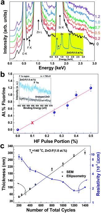 |
| | Fig. 3 (a) EDX spectra of undoped ZnO and ZnO:F thin films with various F contents. The inset is the EDX results for ZnO:F(1.0) films in the logarithmic scale. (b) Evolution of atomic fluorine concentration as a function of the HF pulse portion. The inset is a high-resolution photoemission spectra of undoped ZnO and ZnO:F(1.0) thin films in the F 1s region. (c) The thickness and resistivity values of ZnO:F(1.0) films deposited on glass substrates at a growth temperature of 140 °C as a function of the number of total cycles. | |
In order to monitor the self-limiting conditions at a deposition temperature of 140 °C and determine the thickness of the films for the optimization of the electrical properties, the thickness and resistivity of the representative ZnO:F thin films (ZnO:F(1.0)) as a function of the cycle number is shown in Fig. 3c. The film thickness increased linearly according to the increase in the number of cycles in the ALD process, and the resistivity decreased significantly up to 1200 total cycles, and increased only slightly thereafter. The lowest resistivity was 1.876 × 10⁻³ Ω cm in the ZnO:F(1.0) thin films processed with 1200 cycles, and the thickness was 287 ± 5 nm as measured by ellipsometry and FE-SEM. The resistivity values were obtained by Hall effect measurements of the films on glass substrates via the van der Pauw method. The thickness of undoped ZnO and ZnO:F films with various concentrations of F is shown in Fig. S1, ESI.† The growth rates of each film are summarized in Table 1. The growth rates of the films were slightly increased with an increase in the concentration of F due to an enhancement in the crystallinity of the films, and a detailed analysis regarding the increase in the growth rate is discussed further with regard to their structural properties.
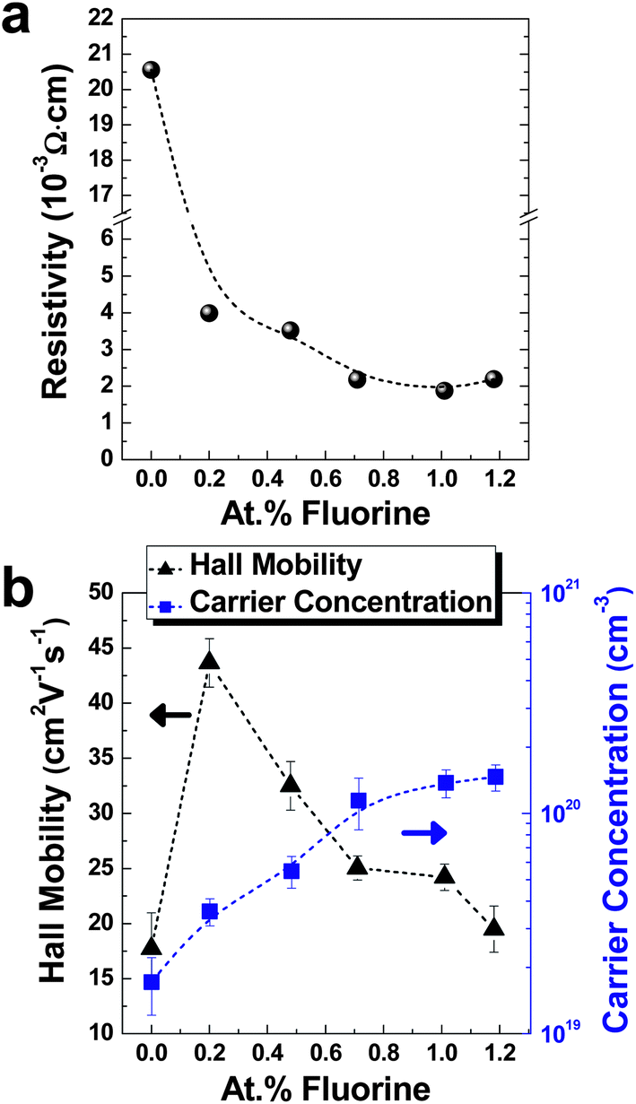
3.2 Electrical properties
The electrical parameters of ZnO:F films with F concentrations ranging from 0 at.% to 1.2 at.% were determined by Hall effect measurements of the films on glass substrates via the van der Pauw method. Fig. 4a and b show plots of resistivity, Hall mobility, and carrier concentration of the samples as a function of the F concentration. The variation in the electrical parameters is summarized in Table S1, ESI.†
 |
| | Fig. 4 (a) Resistivity of the undoped ZnO and ZnO:F films with various F contents deposited on glass substrates at a growth temperature of 140 °C and (b) Hall mobilities and carrier concentrations of the films as a function of atomic fluorine concentration. | |
With an increase in the F concentration, the carrier concentration gradually increased in the range from 1.713 × 1019 cm−3 to 1.462 × 1020 cm−3. These concentration values with F doping are well matched with previously reported values in ZnO:F films7,10,14 and relatively low when compared with cation doping in ZnO, such as with ZnO:Al and ZnO:Ga, which have higher concentrations of up to ∼1021 cm−3.19,20 In the case of cation-doped ZnO films, the electron carriers are simultaneously occupied by Zn substitution of group III ions and native O vacancies, while F ions substitute the O sites in the ZnO lattice. Therefore, ZnO:F films have a relatively low concentration compared to cation-doped ZnO films. On the other hand, films doped with cations typically show lower mobilities, under 20 cm2 V−1 s−1, than ZnO:F films.19,20 In this work, the mobility of ZnO:F films varied from 19.49 cm2 V−1 s−1 to 43.66 cm2 V−1 s−1 with F concentration. Due to the low formation energy of the O vacancy, O sites are favorable doping sites for F ions, as they have a similar ionic radius to that of O2−.9 The conduction band of ZnO is composed of empty 4s levels of Zn2+ ions (from ionic characteristics) or of the lowest anti-bonding sp3 hybrid states (from covalent characteristics). In the same manner, the valence band of ZnO originates from the filled 2p levels of O2− ions or the energetically highest bonding sp3 states. Therefore, this behavior of substitution for O, rather than Zn, would relatively prevent the perturbation in the conduction band compared with metal dopants, which substitute Zn. This effect leads to a dramatic increase in mobilities from 17.73 cm2 V−1 s−1 for undoped ZnO films to 43.66 cm2 V−1 s−1 for ZnO:F{0.2} films at the low doping concentration region. According to an increase of degeneracy of the ZnO:F films with an increase in the F doping concentration, however, F dopants could also act as centers of ionized impurity scattering by contributing to an increase in free electrons because the addition of F− anions raises the Fermi level of ZnO:F films to the conduction band due to filled unoccupied states in conduction bands. Therefore, the mobilities were monotonically decreased from ZnO:F{0.2} films to ZnO:F(1.2) films. Through a combination of carrier concentration and mobility, the lowest resistivity value obtained was 1.876 × 10⁻³ Ω cm for ZnO:F(1.0) films when the carrier concentration and mobility were 1.375 × 1020 cm−3 and 24.20 cm2 V−1 s−1, respectively. The highest resistivity value, as expected, was 2.055 × 10⁻² Ω cm for undoped ZnO films and the carrier concentration and mobility were 1.713 × 1019 cm−3 and 17.73 cm2 V−1 s−1, respectively. In order to check the effectiveness of F in the ZnO matrix as a dopant, the doping efficiency (ηDE) was calculated under the assumption that every incorporated F− ion provides one free electron with substitution of an O2− ion. The ηDE value is defined as the ratio of the electron concentration to the F atomic concentration in the ZnO:F film, which is supposed to have the density of 5.606 g cm−3 similar to that of the bulk ZnO.7 The physical meaning of ηDE provides the fraction of the electrically activated F atoms to F atoms doped in the film. The highest ηDE value was 21.6% for the ZnO:F{2.0} film and the ηDE value of the ZnO:F(1.0) film (lowest resistivity in this work) was 16.4%. These values are relatively lower than previously reported values as high as 65–97% for CVD-grown ZnO:F films at 375 °C–450 °C by Hu et al.7 This might have resulted from the very high growth temperature, higher than 140 °C, in this work, which leads to easy activation of F dopants in the films. On the other hand, Lee et al. reported the electron concentration of 1.4 × 1020 cm−3 and 1.9 × 1020 cm−3 for the ZnO:Al film with 1.9 at.% Al (the lowest resistivity) and with 3.4 at.% Al (the highest carrier concentration) deposited by ALD at 200 °C, respectively.4 From this information, the ηDE values of the films could be calculated as 8.7% and 6.5%, respectively, because an Al3+ ion donates one electron in the ZnO:Al film with substitution of a Zn2+ ion similar to F doping. These ηDE values for ZnO:Al films are smaller than those of ZnO:F films even if the films were grown at a relatively higher temperature (200 °C). These low ηDE values of ZnO:Al films are clearly considered by the laminated structure of ZnO and Al2O3 alloys from the Al doping process by ALD, while a laminated structure is not necessary to incorporate the F atoms into the ZnO matrix in this work as mentioned in the Introduction section. And also, the effectiveness of F as a dopant material for ZnO films is clearly confirmed from this result.
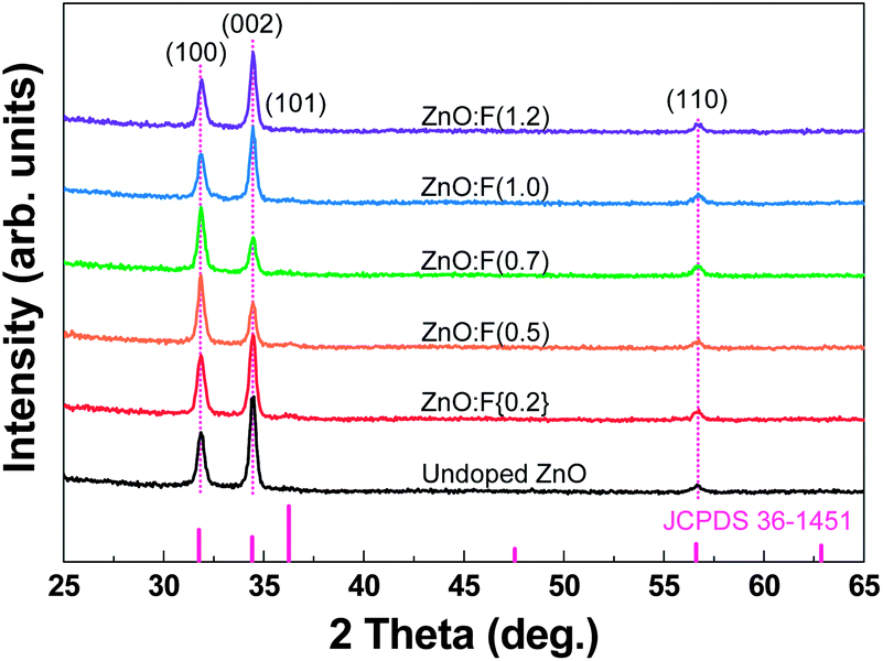
3.3 Structural and morphological properties and GIWAXD study
Crystal structures of undoped ZnO and ZnO:F films with various doping contents grown on glass substrates were analyzed by XRD. The XRD spectra of the films grown by 1200 total ALD cycles at a constant substrate temperature (140 °C) are shown in Fig. 5. The main diffraction peaks of all films at 2θ angles of 31.74°, 34.46°, and 56.60° were indexed as (100), (002), and (110), respectively, agreed with the standard diffraction pattern (JCPDS 36-1451) of a hexagonal wurtzite ZnO structure. The crystal growth of the ALD-grown ZnO films is mainly influenced by growth temperature.21 In our experimental conditions, the preferred orientation peaks were a mixture of (100) and (002), and this result was well matched with previous work by Pung et al.21 By using the well known Scherrer equation, the calculated average grain sizes of the samples by using the full-width at half-maximum of (100) and (002) peaks were summarized in Table S1, ESI.† The average grain sizes of the sample were ranged from 19 nm to 24 nm without particular tendency according to the F doping concentration because the films were deposited at a constant temperature of 140 °C. The change in the preferential orientation between (100) and (002), however, may be explained by the F concentration. At the same deposition temperature, an increase in the F doping concentration from 0 at.% to 0.2 at.% leads to a (002) preferred orientation. With a further increase in the F concentration from 0.5 at.% to 0.7 at.%, the preferred orientation was changed from (002) to (100), and that of the films doped with more than 1.0 at.% was changed from (100) to (002). This change in the preferred orientation of ZnO thin films according to the F doping concentration at the same deposition temperature has not been reported previously, as ZnO:F films exhibit a hexagonal structure with a strongly preferred (002) oriented plane due to growth or post-annealing by pulsed laser deposition,13 radio frequency magnetron sputtering,14 electron beam evaporation,10 and CVD7 at high temperatures of over 450 °C. Liu et al. previously reported first-principles studies of ZnO:F and suggested that the most favorable sites for F doping into a ZnO matrix are O vacancies, which have the lowest formation energy and act as the dominant defect species.9 Therefore, it is anticipated that the growth of the a-axis-oriented (100) plane is more active than the growth of the c-axis-oriented (002) planes perpendicular to the substrate due to F− anions filling O vacancies or substituting O sites as the F doping concentration increases. Moreover, ZnO:F films have a saturation point of F doping into the ZnO matrix, and thus it is apparent that the preferred (100) orientation was changed to the preferred (002) orientation as the F doping concentration increased above 0.7 at.%. This fact explained the morphology of the ZnO and ZnO:F films as well as the XRD patterns. A change in the peak position resulting from lattice distortion with F doping was not observed because the ionic radius of the F− anion (∼1.31 Å) is very similar to that of the O2− anion (∼1.38 Å) when F− anions fill oxygen defect sites.
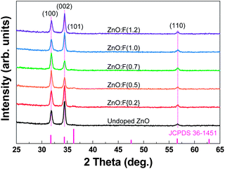 |
| | Fig. 5 Overlay of XRD patterns of undoped ZnO and ZnO films with various F contents deposited at a growth temperature of 140 °C on glass substrates. | |
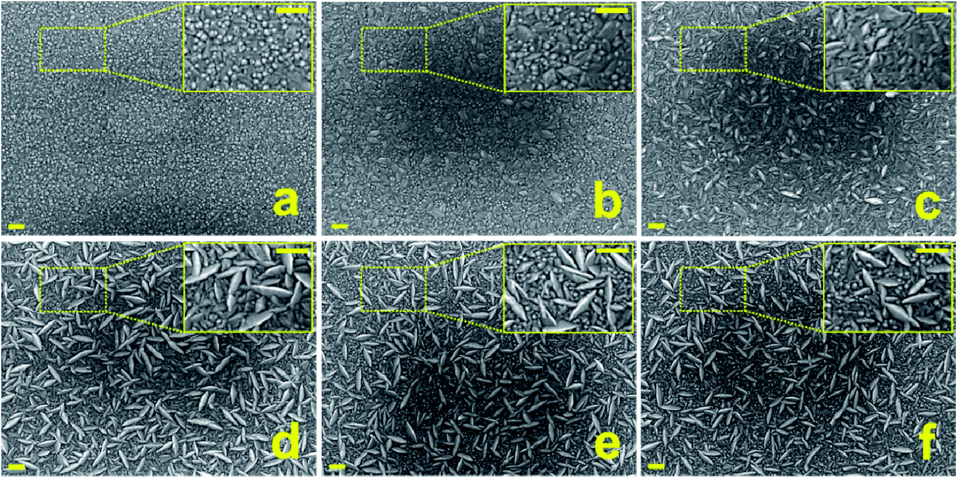
The surface morphology of ZnO and ZnO:F thin films with various F concentrations deposited on glass substrates by ALD was investigated by FE-SEM, and the resulting images are shown in Fig. 6. The undoped and doped ZnO films made at the same deposition temperature (140 °C) exhibited a surface structure consisting of grains of different sizes and morphologies that were strongly dependent on the F doping concentration. Normally, columnar and wedge-like morphologies are regarded as c-axis and a-axis growth orientations, respectively.22
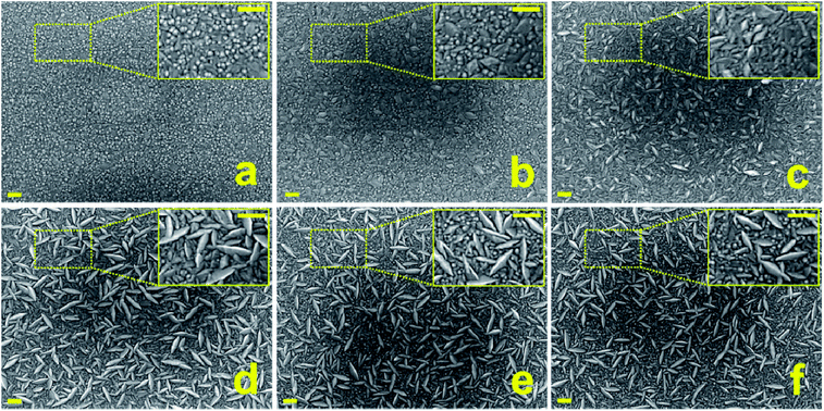 |
| | Fig. 6 Top view FE-SEM images of (a) undoped ZnO, (b) ZnO:F{0.2}, (c) ZnO:F(0.5), (d) ZnO:F(0.7), (e) ZnO:F(1.0), and (f) ZnO:F(1.2) films grown at 140 °C on glass substrates (all scale bars represent 200 nm). | |
Undoped ZnO thin films grew with a c-axis orientation. With an increase in the F content, the c-axis-oriented grains decreased and the a-axis-oriented grains increased up to ZnO:F(0.7). When the F-doping concentration increased to 0.7 at.%, the grains of the films were largely wedge-like in shape, suggesting that the (100) planes have further growth than (002) planes, which is consistent with the XRD analysis. Moreover, it seems that these phenomena were saturated in ZnO:F(0.7) thin films. Columnar grains increased from ZnO:F(1.0) to ZnO:F(1.2). This morphological change with respect to the F doping concentration might be the result of the F doping mechanism, and is not influenced by the difference in grain growth with temperature as films were grown at a constant temperature. There was good evidence that F− anions could passivate surface dangling bonds. In fact, in nanocrystalline thin films of ZnO, the high number of surface dangling bonds can act as trap sites for free electron carriers and therefore decrease the mobility, which subsequently leads to an increase in resistivity. Therefore, this passivation effect, through saturating these surface dangling bonds by F− anions at grain boundaries, might result in a drastic increase in the mobilities from 17.73 cm2 V−1 s−1 for undoped ZnO films to 43.66 cm2 V−1 s−1 for ZnO:F{0.2} films with a slight increase in the carrier concentration from intrinsic ZnO to ZnO:F{0.2} films. In solar cell applications, a textured transparent electrode surface is a necessary precondition for light trapping, as this enhances the light absorption and solar efficiency of active cells. In current commercial applications, the surface texture is developed by the post-deposition wet-etching of smooth, deposited ZnO films.23 The approach of fabricating textured ZnO:F films presented here has potential for use in light-trapping applications through a single-step process without wet-chemical etching, and may also be adopted for flexible substrates that require a low deposition temperature.
There are limitations of the analysis based on the XRD patterns and surface morphologies of the films in understanding the growth modes of ZnO:F films according to the increasing F doping concentration. Thus, a GIWAXD study was performed to better understand the growth mechanism because the information depth in a GIWAXD study could totally cover the thickness of ZnO:F films according to the growth direction (Si substrate peaks could be detected in the experiments). Fig. 7 shows the GIWAXD patterns of the 2D image and 1D scattering intensity curves (the detection angles are 10°, 45°, and 90° from the Si substrate) for (a) undoped ZnO and (b–f) various ZnO:F films grown at 140 °C on Si substrates. To determine the 2D intensity distribution, the horizontal (or out-of-plane) component of the scattering vector qy was plotted along the x-axis, and the vertical (or in-plane) component of the scattering vector qz was plotted along the y-axis. The observed diffraction peaks were addressed according to the Miller indices (hkl). When the growth component perpendicular to the substrate was considered, the growth mode of the undoped ZnO films (Fig. 7a) showed a similar behavior to that suggested by the XRD results. However, with an increase in the F doping concentration, the growth of (100) planes increased up to an F concentration of 0.7 at.% (Fig. 7c), after which the growth of the (100) planes was saturated. When the concentration of F exceeded 0.7 at.%, the intensity of the (100) planes did not change, then the growth of (002) planes increased up to the maximum F doping concentration (ZnO:F(1.2) films). Based on these results, the assumed growth mode of the ZnO:F films as determined via XRD and morphological analysis could be confirmed. F− anions preferentially substitute for O2− anion sites and O vacancies with the growth of (100) planes, and preferential filling continues with the growth of (002) planes in the longitudinal direction of the hexagonal wurtzite structure as the F doping concentration increases. Therefore, it is suggested that diminishing O-related defect sites in ZnO:F films lead to the enhancement of the growth rate of the films.
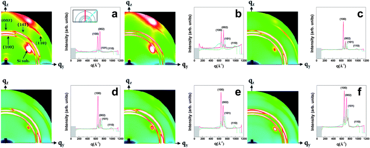 |
| | Fig. 7 GIWAXD patterns of the 2D image and 1D scattering intensity curves of (a) undoped ZnO, (b) ZnO:F{0.2}, (c) ZnO:F(0.5), (d) ZnO:F(0.7), (e) ZnO:F(1.0), and (f) ZnO:F(1.2) films grown at 140 °C on Si substrates. For the 2D intensity distribution, the horizontal (or out-of-plane) component of the scattering vector qy is plotted along the x-axis, and the vertical (or in-plane) component of the scattering vector qz is plotted along the y-axis. The observed diffraction peaks are addressed according to Miller indices (hkl). | |
3.4 Photoluminescence and optical properties
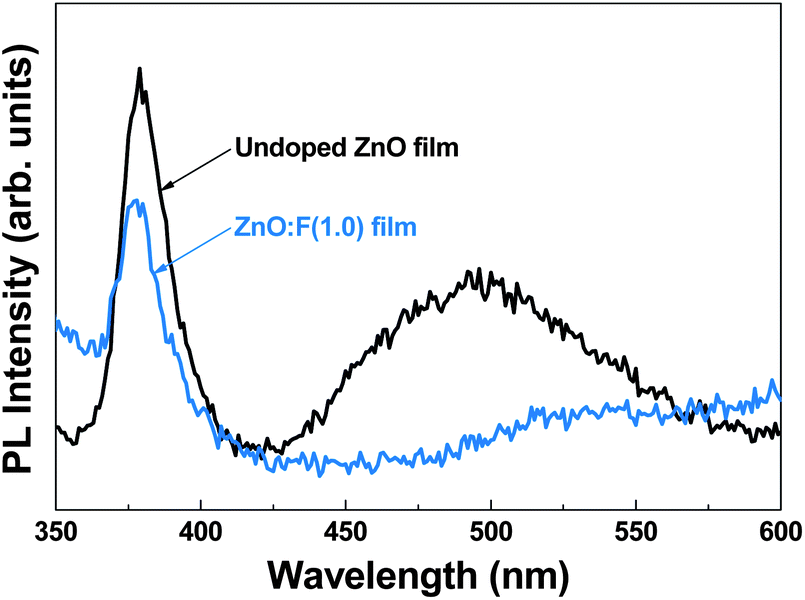
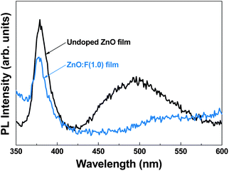
In order to confirm the structural-defect-related properties associated with the aforementioned growth mode, room temperature PL spectra for undoped ZnO and representative ZnO:F(1.0) thin films grown at 140 °C on Si substrates, which showed the minimum resistivity, were monitored and are shown in Fig. 8. Both films exhibited a strong luminescence peak at ∼379 nm for undoped ZnO and ∼377 nm for ZnO:F(1.0) films, the position of which is known as the near-band-edge (NBE) transition. A broader emission band centered at ∼500 nm was located in the green emission portion of the visible region, which can be explained by deep level defects such as O vacancies and Zn interstitials in the ZnO crystals.24,25 Therefore, the significant abatement of the intensity of visible emissions is likely a result of the decrease in O vacancies, which can be attributed to the F− anions that occupy the empty sites in the ZnO matrix.26 This result is well matched with previous PL analyses of ZnO:F films26,27 and the results the XRD and GIWAXD analyses presented in this work. In order to confirm the enhancement of crystal quality due to F doping, the IUV/IVIS ratio was calculated, where IUV and IVIS are the intensities of the UV and visible emission peaks, respectively. The calculated values of IUV/IVIS for undoped ZnO and ZnO:F(1.0) films were 1.740 and 2.609, respectively. This indicated that the ZnO:F(1.0) films had better crystallinity and fewer defects than the undoped ZnO films due to the substitutional doping of O ions with F ions and the filling of O-related defect sites. This resulted in an increase in the growth rate with increases in the F concentration in ZnO crystals, even at low temperatures.
 |
| | Fig. 8 PL spectra of undoped ZnO and ZnO:F films deposited on glass substrates at 140 °C. The spectra were measured at room temperature with a laser excitation wavelength of 325 nm. | |
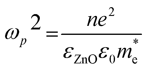
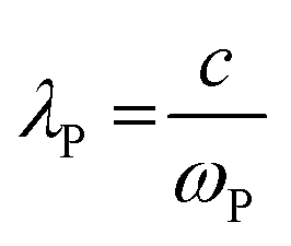
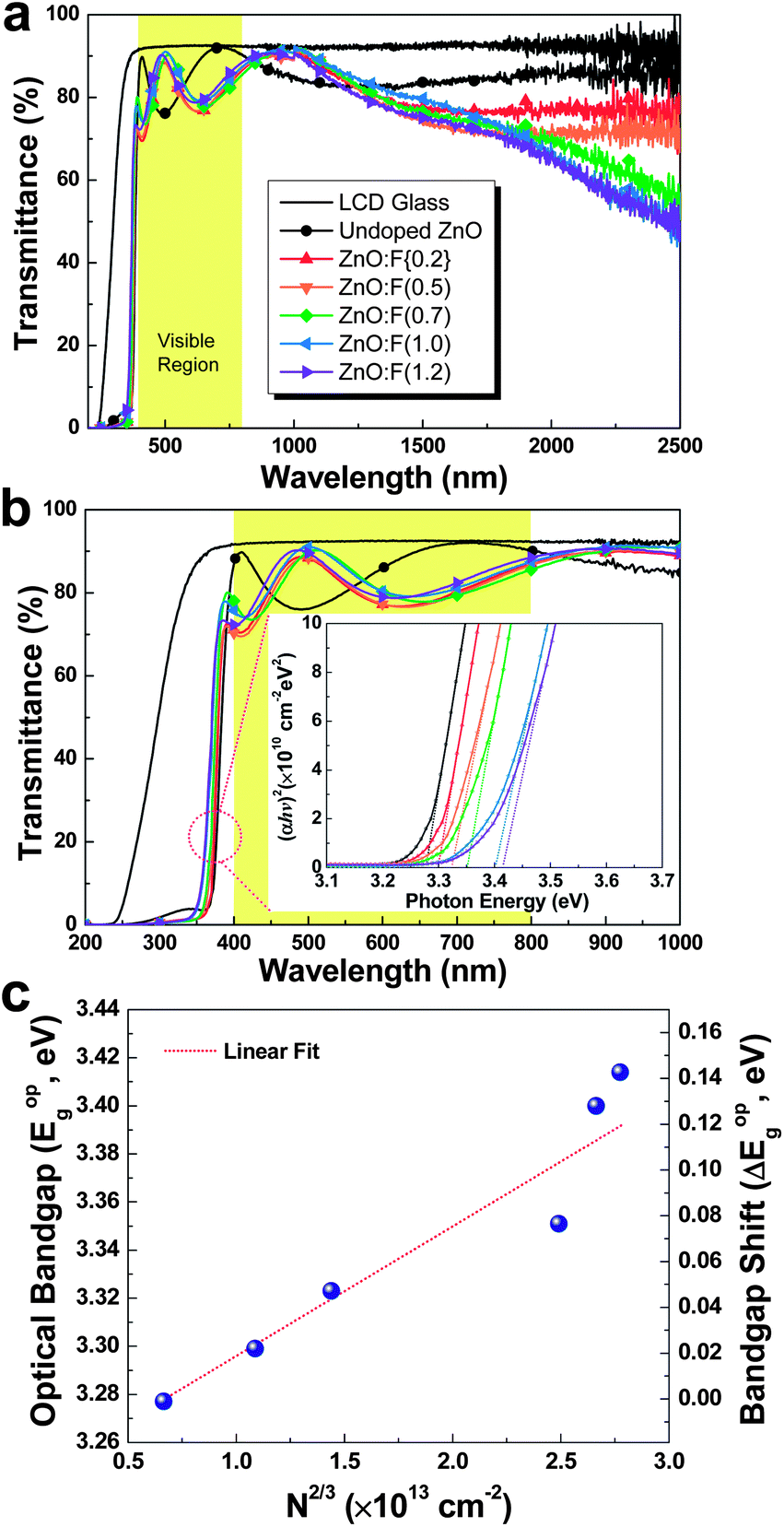
Fig. 9 shows the optical transmittance of undoped ZnO and various ZnO:F films from 200 nm to 2500 nm (Fig. 9a) and the visible range from 200 nm to 1000 nm (Fig. 9b). In TCOs, the three main regions of transmittance are typically divided into ultra-violet (UV), visible, and near-infrared (NIR). As the carrier concentration of the films increased through F doping in ZnO, the absorption was increased in the NIR region. This phenomenon can be explained by the classical Drude free-electron theory. In other words, absorption by free electrons restricts the transmittance of films with high electron density in the conduction band such that the absorption and reflection of electron gas (plasmon) increases and the transmittance decreases for frequencies lower than the plasma frequency (for wavelengths higher than the plasma wavelength) as follows:
| |  | (6) |
| |  | (7) |
where
ωP is the plasma frequency;
n is the electron concentration;
e is the electron charge;
εZnO and
ε0 are the dielectric constants measured in the transparent region of the spectrum of undoped ZnO and the vacuum permittivity;
λP is the plasma wavelength; and
c is the velocity of light in a vacuum.
28 Therefore, with an increase in the carrier concentration with an increase in the F doping concentration, the absorption of the films was increased by the shortening of the plasma wavelength. These results are well matched with the electrical properties of ZnO and the various ZnO:F films. In the literature,
29 the plasma wavelengths of ZnO:F and ZnO:Al (representative cation-doped ZnO) films were reported to be greater than 2000 nm and 1300 nm, respectively. Therefore, this result demonstrated the superiority of ZnO:F films compared with cation-doped ZnO films; namely, the higher mobility of the ZnO:F films led to low resistivity even though the carrier concentration was lower than in cation-doped ZnO films. This yields films that are suitable for applications in solar cells for long wavelength light absorption.
 |
| | Fig. 9 (a) The optical transmittance ranging from 200 nm to 2500 nm of undoped ZnO and ZnO:F films with various F contents deposited on glass substrates at 140 °C. (b) The enlarged transmittance of the visible range for undoped ZnO and ZnO:F films with various F contents. The inset is a plot for the evaluation of the optical band gap of the films. (c) The dependence of the optical band gap and band gap shift of the films on the carrier concentration (n2/3). The dotted line represents the linear fit of experimental results. | |
The average transmittance values in the visible light region (from 380 to 780 nm) of the undoped ZnO, ZnO:F{0.2}, ZnO:F(0.5), ZnO:F(0.7), ZnO:F(1.0), and ZnO:F(1.2) films were 79.93%, 81.01%, 80.58%, 81.76%, 82.99%, and 83.03%, respectively. Similarly to other reported results,14 the optical transmittance of the ZnO:F films in the range from 380–780 nm was slightly enhanced with increased F content. This result could be explained by a more facile electron transition for absorbing photon energy in the short wavelength region with increasing F anion concentration in the ZnO matrix. Furthermore, the occupation of O2− sites by F− anions could result in a decline in O vacancies, which could decrease absorption and emission in the visible region as a result of the O defects. The transmittance of the films on glass substrates was consistently higher than 80%, which is suitable for transparent electrodes. The visible region from 500 nm to 550 nm is known to be the region of maximum absorption in organic solar cells, and the transmittance of all ZnO:F films reached nearly 90%, which is the same as an LCD glass substrate. Therefore, the ZnO:F thin film developed in this work could possibly serve as transparent electrodes for organic solar cells due to the high transparency at the maximum absorption wavelength.
To further investigate the optical behavior of ZnO:F thin films in the UV region, the absorption coefficient was calculated using Lambert's formula:
| |  | (8) |
where
t and
Tr are the film thickness and transmittance, respectively.
30 The direct band gaps of the films were estimated from the (α
hv)
2vs.
hv (Tauc relationship) plot by extrapolating the fit of the linear region to
α = 0, shown in the inset of
Fig. 9b. The estimated optical band gap values increased with increasing F content and the values of the undoped ZnO, ZnO:F{0.2}, ZnO:F(0.5), ZnO:F(0.7), ZnO:F(1.0), and ZnO:F(1.2) films were 3.277 eV, 3.299 eV, 3.323 eV, 3.351 eV, 3.400 eV, and 3.414 eV, respectively. Furthermore, the shift in the absorption edge increased with increasing amounts of F. The band gap of the ZnO film, 3.277 eV, was in agreement with the ideal band gap of pure ZnO.
1 The increase in the band gap with respect to the increasing F content is generally believed to be due to the Burstein–Moss effect.
31,32 ZnO films are n-type oxide semiconductors due to the electron donors generated by O vacancies and Zn interstitials. The addition of donor F
− anions raises the Fermi level of the ZnO:F films into the conduction band, causing the films to completely degenerate, and the absorption edge therefore moves to an energy higher than the actual band gap of pure ZnO. Finally, the monotonic increase in the absorption in the NIR region and the optical band gap in the UV region could be considered to be additional evidence of the increase in electron concentration as the F doping concentration increases. In order to verify the optical band gap widening in ZnO:F films by Burstein–Moss effect, the dependence of the band gap shift on the electron concentration,
n2/3, is presented in
Fig. 9c. Assuming the parabolic energy band, and due to the direct-band gap of ZnO, the optical band gap widening can be presented by the energy
33| |  | (9) |
where
h is Plank's constant,
m* is the reduced effective mass, and
n is the electron concentration in ZnO and ZnO:F films. In
Fig. 9c, the optical band gap shift is observed to be directly proportional to
n2/3 by linear fitting of the experimental results. The slope of the linear fitting line yields
m* = 0.62
m0, where
m0 is the free electron mass in free space. This
m* value is similar to the previously reported one, which are 0.60
m0 for ZnO:F films
13 and 0.55
m0 for ZnO:Ga films.
34 This
m* value is higher than the theoretical reduced effective mass of 0.19
m0 (1/
m* = 1/
m*e +1/
m*h, where
m*e and
m*h represent the electron effective mass (0.28
m0) and hole effective mass (0.59
m0)) for ZnO.
35 The enhancement of the effective mass might be caused by a possible nonparabolicity effect of the ZnO conduction band and also, band gap renormalization with the degeneracy of the films by an increase of the electron concentration in the conduction band.
36
4 Conclusions
A simple method of F doping into a ZnO matrix using ALD was demonstrated. The deposition temperature of the ZnO:F films was very low (140 °C), yet still yielded excellent electrical and optical performances compared with other reported methods that require growth temperatures over 450 °C. Through the increased F doping into the ZnO matrix, the grain growth orientation was changed from c-axis to a-axis and then from a-axis to c-axis. This F doping phenomenon could be explained by the substitution of O sites with F anions, which was corroborated by the XRD, surface morphology, and GIWAXD analysis. Moreover, the growth mode of the ALD-ZnO:F films was confirmed by GIWAXD analysis. Along with the increase in the F doping concentration, the optical transmittance of the films increased slightly from 80.97% to 83.02% due to a decrease in the absorption in the visible region by F anions filling O defects. The Burstein–Moss effect may also explain to the higher transparency of the films through the band gap widening effect with the increase in the carrier concentration induced by the increase in the F doping concentration. The electron carrier concentration was gradually increased from 1.713 × 1019 cm−3 to 1.462 × 1020 cm−3 by the increase in the F concentration in the films. The Hall mobility was maximized at 43.66 cm2 V−1 s−1 with a low concentration of F doping of approximately 0.20 at.%. A minimum resistivity value of 1.876 × 10⁻³ Ωcm was obtained in ZnO:F(1.0) films, and the carrier concentration and mobility were 1.375 × 1020 cm−3 and 24.20 cm2 V−1 s−1, respectively. Therefore, it was confirmed that the novel fabrication method of ZnO:F thin films using ALD and an adjusted F doping concentration could be optimized for a growth temperature of 140 °C, which remained the optimized growth temperature for the ZnO:F thin films at a fixed F concentration.
Acknowledgements
This work was supported by the National Research Foundation of Korea (NRF) grant funded by the Korea government (MEST) (no. 2012R1A2A2A01011014). Experiments at PLS were supported in part by MEST and POSTECH.
Notes and references
- D. S. Ginley and C. Bright, MRS Bull., 2000, 25, 15 CrossRef CAS.
- E. Fortynato, D. Ginley, H. Hosono and D. C. David, MRS Bull., 2007, 32, 242 CrossRef.
- Y.-J. Choi, S. C. Gong, C.-S. Park, H.-S. Lee, J. G. Jang, H. J. Chang, G. Y. Yeom and H.-H. Park, ACS Appl. Mater. Interfaces, 2013, 5, 3650 CAS.
- D.-J. Lee, H.-M. Kim, J.-Y. Kwon, H. Choi, S.-H. Kim and K.-B. Kim, Adv. Funct. Mater., 2011, 21, 448 CrossRef CAS.
- H. Serier, A. Demourgues and M. Gaudon, Inorg. Chem., 2010, 49, 6853 CrossRef CAS PubMed.
- B. Sang, A. Yamada and M. Konagai, Sol. Energy Mater. Sol. Cells, 1997, 49, 19 CrossRef CAS.
- J. Hu and R. G. Gordon, Sol. Energy Mater. Sol. Cells, 1991, 30, 437 CAS.
- J. Rousset, E. Saucedo and D. Lincot, Chem. Mater., 2009, 21, 534 CrossRef CAS.
- B. Liu, M. Gu, X. Liu, S. Huang and C. Ni, Appl. Phys. Lett., 2010, 97, 122101 CrossRef.
- H. Y. Xu, Y. C. Liu, R. Mu, C. L. Shao, Y. M. Lu, D. Z. Shen and X. W. Fan, Appl. Phys. Lett., 2005, 86, 123107 CrossRef.
- S. Ilican, Y. Caglar, M. Caglar and F. Yakuphanoglu, Appl. Surf. Sci., 2008, 255, 2353 CrossRef CAS.
- M. L. Olvera, A. Maldonado and R. Asomoza, Sol. Energy Mater. Sol. Cells, 2002, 73, 425 CrossRef.
- L. Cao, L. Zhu, J. Jiang, R. Zhao, Z. Ye and B. Zhao, Sol. Energy Mater. Sol. Cells, 2011, 95, 894 CrossRef CAS.
- H. S. Yoon, K. S. Lee, B. Cheong, D. K. Choi, D. H. Kim and W. M. Kim, Sol. Energy Mater. Sol. Cells, 2008, 92, 1366 CrossRef CAS.
- T. Pilvi, K. Arstila, M. Leskela and M. Ritala, Chem. Mater., 2007, 19, 3387 CrossRef CAS.
- T. Pilvi, E. Puukilainen, U. Kreissig, M. Leskelä and M. Ritala, Chem. Mater., 2008, 20, 5023 CrossRef CAS.
- J.-S. Na, Q. Peng, G. Scarel and G. N. Parson, Chem. Mater., 2009, 21, 5585 CrossRef CAS.
- J. W. Elam and S. M. George, Chem. Mater., 2003, 15, 1020 CrossRef CAS.
- P. Banerjee, W.-J. Lee, K.-R. Bae, S. B. Lee and G. W. Rubloff, J. Appl. Phys., 2010, 108, 043504 CrossRef.
- A. Segura, J. A. Sans, D. Errandonea, D. Martinez-García and V. Fages, Appl. Phys. Lett., 2006, 88, 011910 CrossRef.
- S.-Y. Pung, K.-L. Choy, X. Hou and C. Shan, Nanotechnology, 2008, 19, 435609 CrossRef PubMed.
- S.-H. Ko Park and Y. E. Lee, J. Mater. Sci., 2004, 39, 2195 CrossRef CAS.
- M. Berginski, J. Hüpkes, M. Schulte, G. Schöpe, H. Stiebig and B. Rech, J. Appl. Phys., 2007, 101, 074903 CrossRef.
- K. Vanheusden, W. L. Warren, C. H. Seager, D. R. Tallant, J. A. Voigt and B. E. Gnade, J. Appl. Phys., 1996, 79, 7983 CrossRef CAS.
- Y.-P. Wang, W.-I. Lee and T.-Y. Tseng, Appl. Phys. Lett., 1996, 69, 1807 CrossRef CAS.
- Y.-Z. Tsai, N.-F. Wang and C.-L. Tsai, Mater. Lett., 2009, 63, 1621 CrossRef CAS.
- H. Y. Xu, Y. C. Liu, J. G. Ma, Y. M. Luo, Y. M. Lu, D. Z. Shen, J. Y. Zhang, X. W. Gan and R. Mu, J. Phys.: Condens. Matter, 2004, 16, 5143 CrossRef CAS.
- T. Wang and P. V. Radovanovic, J. Phys. Chem. C, 2011, 115, 406 CAS.
- R. G. Gordon, MRS Bull., 2000, 25, 52 CrossRef CAS.
- S. T. Tan, B. J. Chen, X. W. Sun, W. J. Fan, H. S. Kwok, X. H. Zhang and S. J. Chua, J. Appl. Phys., 2005, 98, 013505 CrossRef.
- E. Burstein, Phys. Rev. Lett., 1954, 93, 632 CAS.
- T. S. Moss, Proc. Phys. Soc., London, Sect. B, 1954, 67, 775 CrossRef.
- H. Q. Le, S. J. Lim, G. K. L. Goh, S. J. Chua and J. Ong, J. Electrochem. Soc., 2010, 157, H196 CrossRef.
- J. A. Sans, J. F. Sánchez-Royo, A. Segura, G. Tobias and E. Canadell, Phys. Rev. B: Condens. Matter Mater. Phys., 2009, 79, 195105 CrossRef.
- B. E. Sernelius, K.-F. Berggren, Z.-C. Jin, I. Hamberg and C. G. Granqvist, Phys. Rev. B: Condens. Matter Mater. Phys., 1988, 37, 10244 CrossRef CAS.
- J. D. Ye, S. L. Gu, S. M. Zhu, S. M. Liu, Y. D. Zheng, R. Zheng and Y. Shi, Appl. Phys. Lett., 2005, 86, 192111 CrossRef.
Footnote |
| † Electronic supplementary information (ESI) available: Cross-sectional FE-SEM images of samples, XPS elemental analysis of ZnO:F{0.2} and ZnO:F(1.2) films, table for grain sizes and Hall parameters of samples. See DOI: 10.1039/c3tc31478b |
|
| This journal is © The Royal Society of Chemistry 2014 |
Click here to see how this site uses Cookies. View our privacy policy here.