A new (TTF)11I8 organic molecular conductor: from single crystals to flexible all-organic piezoresistive films†
Victor
Lebedev
a,
Elena
Laukhina
*b,
Evelyn
Moreno-Calvo
ab,
Concepció
Rovira
ab,
Vladimir
Laukhin
abc,
Ivan
Ivanov
d,
Sergei M.
Dolotov
d,
Valery F.
Traven
*d,
Vladimir V.
Chernyshev
ef and
Jaume
Veciana
*ab
aInstitut de Ciencia de Materials de Barcelona (ICMAB-CSIC), Campus UAB, Bellaterra, Spain. E-mail: vecianaj@icmab.es
bCIBER de Bioingeniería, Biomateriales y Nanomedicina (CIBER-BBN), Spain. E-mail: laukhina@icmab.es
cInstitució Catalana de Recerca i Estudis Avançats (ICREA), Barcelona, Spain
dMendeleev University of Chemical Technology, Miusskaya sq., 9, Moscow, Russia. E-mail: traven@muctr.ru
eDepartment of Chemistry, M.V. Lomonosov Moscow State University, GSP-1, Leninskie Gory, 1–3, Moscow, Russia
fA.N. Frumkin Institute of Physical Chemistry and Electrochemistry RAS, Leninsky prospect, 31, Moscow, Russia
First published on 22nd October 2013
Abstract
This paper reports selective synthesis of two iodine-containing TTF (tetrathiafulvalene) salts: one, (TTF)11I8, is a new molecular conductor while another is the known non-conducting (TTF)I3 compound. Single crystals of both salts were prepared using different amounts of iodine in the redox process between TTF and I2. X-ray data showed that the resulting conducting (TTF)11I8 salt might be considered as a new modulated phase of the non-stoichiometric (TTF)I0.7+δ salts. The electrical resistance of single crystals of (TTF)11I8 reveals a semiconducting-like behaviour. The paper presents also a study of electromechanical properties of organic conductive bi-layer (BL) films prepared by covering different organic polymeric films with a thin network of oriented submicrocrystals of (TTF)I0.7+δ phases. These BL films exhibit a combination of flexibility, lightweight, and high piezo-resistivity properties showing therefore a potential interest for electronic sensing applications where lightweight, large area coverage and flexibility are required.
1. Introduction
Economical growth needs to come from the development of new materials and innovative technologies. Novel materials that arouse a great deal of interest are those suitable for electronic applications and in particular for low cost, large area and flexible electronics. The development of flexible, lightweight and conductive materials, whose electrical transport properties strongly respond to small deformations, brings great opportunities in the field of strain, pressure or bending sensors for their applications as human–machine interfaces, intelligent textiles, robotic interfaces and body sensing devices.1–3 One attractive design principle for such materials is the covering of plastic substrates with thin polycrystalline layers of organic molecular metals and semiconductors due to the following reasons.4–7 First, the softness of molecular conductors6,8 provides them with a high piezosensitive effect9 and, hence, it is possible to tune the electrical response to deformations by the chemical modification of their molecular and crystalline structures. Second, the electrical properties of the crystals of organic molecular conductors show good long-term stability – more than 10 years stability – when stored under ambient conditions. Third, covering polymeric films with molecular conductors has already been developed as a simple and low-cost method since it just consists of one step under ambient conditions.4,10 This process is based on the physical and chemical properties of organic molecular conductors and occurs in the immediate region of the swollen surface of a polymeric film.4 It should be noted that two dimensional (2D) organic molecular conductors based on BEDT-TTF [BEDT-TTF = bis(ethylenedithio)tetrathiafulvalene] have been successfully used for engineering flexible sensing bilayer (BL) films with electrical detection principle.7,11–13 These results have opened several promising research avenues permitting the integration of BL films as flexible sensors in medical devices14 and textiles.15 In relation to this topic, iodine-containing TTF (tetrathiafulvalene) salts, as highly conductive organic solids, are also attractive for engineering sensing BL films because of two reasons. First, the conductive sensing layers based on these salts may be formed at the surface of polymeric films using the above-mentioned chemical deposition method since it is known that iodine oxidation yields a variety of conducting charge-transfer salts, such as (TTF)I0.7+δ.16–21 Second, the use of TTF instead of BEDT-TTF may significantly reduce the cost of sensing films because the gram-scale production of TTF is less expensive than BEDT-TTF.22Here we present the synthesis and structural data of a new conductive charge-transfer phase of the non-stoichiometric (TTF)I0.7+δ family of salts, the (TTF)11I8 phase, as well as its electronic transport properties over a wide range of temperatures. Also, we demonstrate that covering polymeric films with thin oriented polycrystalline layers of (TTF)I0.7+δ yields a flexible lightweight piezoresistive material. The paper additionally presents and discusses experimental data on the relationship between the nature of polymeric matrices and main characteristics of polycrystalline covering layers based on the (TTF)I0.7+δ salts.
2. Experimental
2.1. Materials
TTF, poly(bisphenol A carbonate), (polycarbonate, PC, average MW ca. 64![[thin space (1/6-em)]](https://www.rsc.org/images/entities/char_2009.gif) 000), cellulose triacetate (CTA), and cellulose acetate propionate (CAP) were purchased from Aldrich. Organic solvents 1,1-dichloroethane (1,1-DCE), benzonitrile (BN), 1,2-dichlorobenzene (o-DCB), and dichloromethane (DCM) of analytical grade from Aldrich were used. The tetrabutylammonium triiodide (n-Bu4NI3) salt was synthesized as previously published.23
000), cellulose triacetate (CTA), and cellulose acetate propionate (CAP) were purchased from Aldrich. Organic solvents 1,1-dichloroethane (1,1-DCE), benzonitrile (BN), 1,2-dichlorobenzene (o-DCB), and dichloromethane (DCM) of analytical grade from Aldrich were used. The tetrabutylammonium triiodide (n-Bu4NI3) salt was synthesized as previously published.23
2.2. Synthesis of iodine-containing TTF salts
| Empirical formula | (TTF)I3 | (TTF)11I8a |
|---|---|---|
| a The same data were obtained for crystals prepared with methods 1 and 2. | ||
| F w, g mol−1 | 1587 | 3263 |
| Crystal system | Monoclinic | Monoclinic |
| Space group | P21/n | C2 |
| Z | 12 | 4 |
| a, Å | 7.79 | 26.38 |
| b, Å | 18.81 | 16.06 |
| c, Å | 9.43 | 24.24 |
| β, deg. | 103.16 | 101.2 |
| V, Å3 | 1345.49 | 10072(1) |
| D calc (g cm−3) | — | 2.5 |
Method 1. Iodine (7.6 × 10⁻⁵ mol) was added to a hot solution (80 °C) of TTF (14.0 × 10⁻⁵ mol) in 30 mL of a 1,1-DCE–BN mixture (50/50 v/v) under argon. Then, the resulting solution was cooled to 25 °C with a rate of 1 deg per hour and the new polymorph (TTF)11I8 was obtained as bar-like black crystals 1 mm in length. The total yield of the crystals was around 70%.
Method 2. n-Bu4NI3 salt (7.1 × 10⁻⁵ mol) was added to a hot solution (80 °C) of TTF (2.4 × 10⁻⁵ mol) in 30 mL of a 1,1-DCE–BN mixture (50/50 v/v) under argon. Then, the resulting solution was cooled down to 25 °C with a rate of 1 deg per hour, and bar-like black crystals of (TTF)11I8 were obtained; the total yield was around 60%.
2.3. Bilayer polymeric films with (TTF)I0.7+δ
Bilayer (BL) films #1, #2 and #3 based on polymers PC, CTA, and CAP, respectively, were prepared according to the procedure described below. First, 1,2-dichlorobenzene solution-casting films 25–30 μm thick, which contained 2 wt% of molecularly dispersed TTF, were prepared on a glass support at 130 °C. Then one of the surfaces of the films was treated with vapors of a saturated solution of I2 in CH2Cl2 during 6–8 min at 23 °C. The binary mixture system: I2/CH2Cl2 solution–I2/CH2Cl2 vapor was used at equilibrium. This treatment resulted in the development of conductive (TTF)I0.7+δ-based covering layers. Detailed data on the covering procedure are presented in the ESI, Fig. S1.†2.4. Characterization of conductive crystalline materials
687 reflections were collected of which 24664 [R(int) = 0.0379] were unique. Programs used: data collection, Smart;24 data reduction, Saint+;25 absorption correction, SADABS.26 Structure solution and refinement was done using SHELXTL.27
The structure of the new polymorph (TTF)11I8 was solved by direct methods and refined by full-matrix least-squares methods on F2. The non-hydrogen atoms were refined anisotropically. The H-atoms were placed in geometrically optimized positions and forced to ride on the atom to which they are attached. The crystal was solved and refined in the C2 space group as a racemic twin. Possible higher symmetry was suspected and trials to find a solution in space group C2/c were made. A possible solution was found, but efforts to refine the structure in C2/c were unsuccessful. Details are given on the refine special details section of the cif file. Final R indices [I > 2θ(I)]: R1 = 0.0406, wR2 = 0.0878; R indices (all data): R1 = 0.1487 and wR2 = 0.1310.†
2.5. Macroscopic electro-transport properties
The values of the room temperature resistance of single crystals and BL films as well as their resistance temperature dependences were measured by a standard four-probe dc-method. In the case of BL films, rectangular pieces (4 × 2 mm2) were cut out from the film samples. Four annealed platinum wires with a diameter of 20 μm were attached to the single crystal or to the conductive covering layer of BL films with a graphite paste.2.6. Electromechanical tests
3. Results and discussion
The ability of iodine to form stable species like I−, I3− and I5− has lead to the formation of multiple phases of charge transfer salts with (TTF)Ix compositions during the oxidation of TTF with I2 in solution.16–21 These salts significantly differ in their conducting properties since the stoichiometric phases (x = 2 and 3) are non-conducting while the non-stoichiometric ones (x = 0.71 and 2.3) behave as one-dimensional highly conducting systems.18 Attempts to prepare selectively the conducting phase (TTF)I0.71, with a TTF7I5 composition, by reacting stoichiometric amounts of TTF with iodine in solution resulted in complex mixtures of phases.18 Therefore, the covering of a polymeric film with a homogeneous crystallite layer of (TTF)I0.71 was a challenge. This drawback made us first determine the best conditions to prepare the pure (TTF)I0.71 phase before attempting to cover polymeric films with its polycrystalline layer.3.1. Selective synthesis of (TTF)I3 and (TTF)11I8 salts
We discovered that there exist optimal reaction conditions, concerning the amount of iodine, solvent, and temperature, which are capable of selectively controlling the formation of crystals of either the (TTF)I3 phase or a new non-stoichiometric phase of (TTF)I0.7+δ type. Interestingly, the oxidation of TTF by a non-equimolar amount of iodine in a 1,1-DCE–BN mixture (50/50 v/v) proceeds with an excellent selectivity, rendering single crystals of (TTF)Ix salts, when a hot reagent solution was cooled from 80 to 25 °C with a cooling rate of 1 deg per hour. Thus, the (TTF)I3 salt18 was obtained when the molar ratio of I2:TTF was 0.9:1 while the new non-stoichiometric phase was selectively formed when the molar ratio was 0.5:1 or lower. Both salts were reproducibly prepared in good yields being stable in air for several months. The new phase of (TTF)I0.7+δ type, that corresponds to the (TTF)11I8 salt (vide infra), can be also prepared pure by mixing solutions of TTF and Bu4NI3, using the later reagent in a large excess. In this case I2 was also the oxidizing agent formed in small amounts due to the well-known dissociation process of I3− into I2 and I−.28
3.2. Characterization of the new (TTF)11I8 phase
The composition of the crystals prepared using methods 1 and 2 was studied by EDX analysis. The S:I stoichiometry determined for several crystals varies from 4:0.70 to 4:0.75; close to the calculated value of S:I = 4:0.7 for the reported (TTF)I0.7+δ salt. Single crystal X-ray diffraction data reveal that these crystals are related to the new (TTF)11I8 member of the non-stoichiometric (TTF)I0.7+δ salts; the crystals of (TTF)11I8 are monoclinic with the chiral space group C2. The crystal structure of the new TTF11I8 salt is close to that of TTF7I5, reported by Johnson et al.29 The crystal structure of the TTF7I5 phase (Fig. 1 top) has the asymmetric unit that contains 15 independent iodide ions and 20 TTF moieties in general positions, and halves of two TTF moieties situated on inversion centers. All TTF moieties in phase TTF7I5 were considered as planar and centrosymmetric, and were used in structure determination and refinement as identical rigid units.18
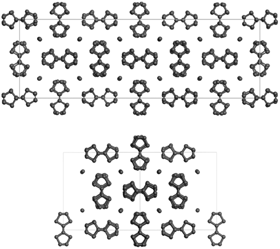 | ||
| Fig. 1 Crystal packing of the TTF7I5 phase viewed along the [001] direction (top) and of the TTF11I8 phase viewed along the [10−1] direction (bottom). The unit cell box is shown for each structure. Hydrogen atoms have been omitted for clarity. | ||
The crystal structure of the (TTF)11I8 phase (Fig. 1, bottom) determined from single crystal X-ray data shows that the structure is modulated showing lateral displacements about the axis along each TTF and iodine columns. The asymmetric unit contains 8 independent iodide ions and 10 TTF moieties in general positions, and halves of two TTF moieties situated on two-fold rotational axes arranged into two columns of five and a half molecules each. The TTF moieties are non-planar being slightly twisted with S–C![[double bond, length as m-dash]](https://www.rsc.org/images/entities/char_e001.gif) C–S torsion angles varying from 0.06(3) up to 2.8(3)°. It is worth mentioning that the crystal packing features of TTF7I5 and TTF11I8 are very close. In both phases TTF moieties are stacked into columns, which propagate in one direction along [10−1] in TTF11I8 and along [001] in TTF7I5. The TTF columns are packed in such a way that they form channels filled with iodine species. As all distances between the iodide atoms in the (TTF)11I8 structure are significantly bigger than those in I2, [I–I⋯I]− and I3− (ESI, Table S1†), the channels between TTF columns are filled with mono atomic iodine anions (I−). Iodide anions have contacts with several sulphur atoms from the neighbouring columns of TTF moieties with I⋯S distances less than the sum of van der Waals radii of I and S [3.8 Å]. Specifically, each iodide anion in TTF7I5 has three of four contacts with I⋯S distances lying in the range 3.53–3.71 Å, while in TTF11I8 iodide anions have from one to four short contacts in the range 3.53–3.73 Å. In spite of close similarity of both TTF7I5 and TTF11I8 phases their crystal structures cannot be transformed into one another, so they are two distinct phases of the non-stoichiometric TTFI0.7+δ type, where δ = 0.014 and 0.027 for TTF7I5 and TTF11I8, respectively. The calculated values of charge transfer based on the bond length ratio showed that the charges on TTF molecules range from +0.700 to +1.295 (ESI, Table S2†). This clearly points out that a conjugative electronic system is formed in the (TTT)11I8 crystals. It should be kept in mind, that the relationship between charge transfer and geometry is only approximate.30
C–S torsion angles varying from 0.06(3) up to 2.8(3)°. It is worth mentioning that the crystal packing features of TTF7I5 and TTF11I8 are very close. In both phases TTF moieties are stacked into columns, which propagate in one direction along [10−1] in TTF11I8 and along [001] in TTF7I5. The TTF columns are packed in such a way that they form channels filled with iodine species. As all distances between the iodide atoms in the (TTF)11I8 structure are significantly bigger than those in I2, [I–I⋯I]− and I3− (ESI, Table S1†), the channels between TTF columns are filled with mono atomic iodine anions (I−). Iodide anions have contacts with several sulphur atoms from the neighbouring columns of TTF moieties with I⋯S distances less than the sum of van der Waals radii of I and S [3.8 Å]. Specifically, each iodide anion in TTF7I5 has three of four contacts with I⋯S distances lying in the range 3.53–3.71 Å, while in TTF11I8 iodide anions have from one to four short contacts in the range 3.53–3.73 Å. In spite of close similarity of both TTF7I5 and TTF11I8 phases their crystal structures cannot be transformed into one another, so they are two distinct phases of the non-stoichiometric TTFI0.7+δ type, where δ = 0.014 and 0.027 for TTF7I5 and TTF11I8, respectively. The calculated values of charge transfer based on the bond length ratio showed that the charges on TTF molecules range from +0.700 to +1.295 (ESI, Table S2†). This clearly points out that a conjugative electronic system is formed in the (TTT)11I8 crystals. It should be kept in mind, that the relationship between charge transfer and geometry is only approximate.30
3.3. Electric transport properties of TTF11I8 crystals
The temperature dependence of four-probe single crystal resistance was measured along the longest axis of the crystal. The magnitude of conductivity at room temperature varies from 50 to 130 Ω−1 cm−1. These values are not too different from those previously reported for single crystals of (TTF)7I5 (100–400 Ω−1 cm−1).18 As Fig. 2 shows, the resistance of TTF11I8 significantly increases with decreasing temperature revealing the change of the slope of R(T) dependence around 200 K. The observed feature related probably to some second order phase transition (which is going to be studied).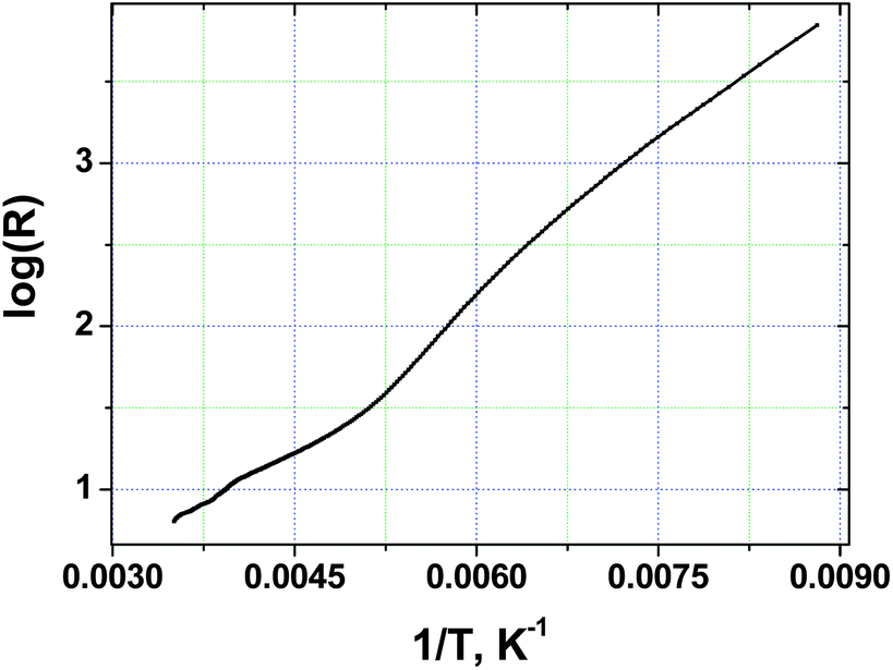 | ||
| Fig. 2 Temperature dependence of electrical resistance for a single crystal of TTF11I8. | ||
3.4. Preparation of bilayer polymeric films with (TTF)I0.7+δ crystals
The simplicity of the oxidation of TTF by a non-equimolar amount of iodine makes this process attractive for engineering conductive TTF-based layers on the surface of polymeric films. With this in mind, we assumed that small amounts of iodine at the swollen surface of a polymeric film may exclusively yield the (TTF)I0.7+δ salts as a conductive covering layer. In line with the BL film preparation method (ESI, Fig. S1†) we first prepared 25–30 μm thick polymeric films containing a 2 wt% of TTF well-dispersed in the polymeric matrix. As matrices we used three different polymers: polycarbonate, PC (film #1); cellulose triacetate, CTA (film #2); and cellulose acetate propionate, CAP (film #3). To cover these films with the polycrystalline layer of (TTF)I0.7+δ we exposed the surface of the films to vapors of a saturated solution of iodine in dichloromethane. The formation of conductive covering layers in the resulting BL films was tested by direct current (dc) resistance measurements.3.5. Characterization of bilayer polymeric films with (TTF)I0.7+δ crystals
The composition of the conductive layers, developed on one side of the polymeric thin films, was studied by EDX analysis. The S:I stoichiometry of the layers formed on the surfaces of films #1, #2 and #3 varies from 4:0.80 to 4:0.89. As these values are reasonably close to the calculated value of 4:0.7 for the (TTF)I0.7+δ salt, we assume that the oxidation of TTF by a non-equimolar amount of iodine occurred in the swollen surfaces of films #1–3 when a short treatment of 6–8 min was used. The conducting layers were also characterized by Raman spectroscopy where a lack of characteristic bands corresponding to νI–I, ν[I–I⋯I]−, ν[I–I⋯TTF]− and ν[I–I–I]− vibration modes was observed.31,32 This result confirms that iodine did not form I3− anions as well as any other iodine-based adducts. Therefore, iodine exists entirely as I− anions in agreement with the structural data for the phases of (TTF)I0.7+δ type.
3.6. Texture of bilayer polymeric films with (TTF)I0.7+δ crystals
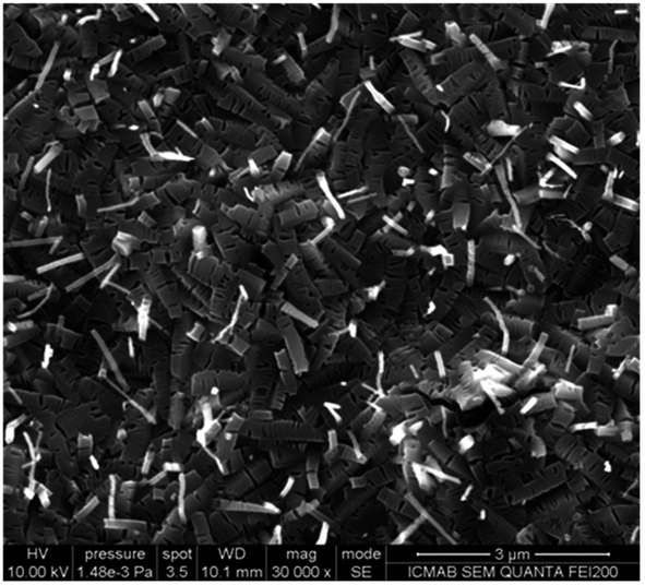
The SEM images of the conductive covering layers of (TTF)I0.7+δ revealed different morphologies for films #1–3 (Fig. 3–5). The image of the conducting layer formed on the surface of film #1 showed the presence of a network of needle-like crystals which have 2 μm length with lateral dimensions ranging from 80 to 200 nanometres (Fig. 3). By contrast, the SEM image of film #2 (Fig. 4) reveals a worm-like aggregation of (TTF)I0.7+δ where the “worms” are mainly connected showing almost identical dimensions to those of needle-like linked crystals of film #1. The SEM image of film #3 showed close-packed plate-like crystals with dimensions of 1 × 0.5 μm2 (Fig. 5).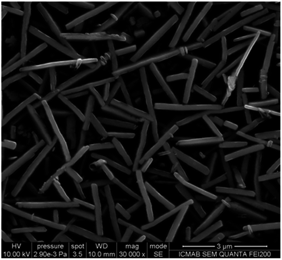 | ||
| Fig. 3 SEM image of the conducting layer of (TTF)I0.7+δ formed on the surface of film #1 (polymeric matrix = PC). | ||
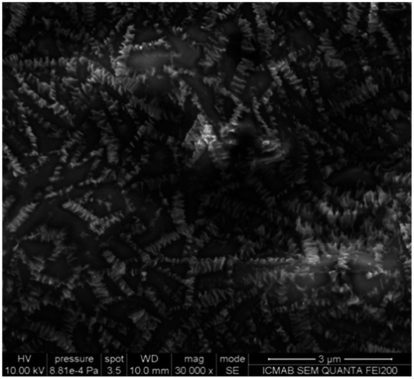 | ||
| Fig. 4 SEM image of the conducting layer of (TTF)I0.7+δ formed on the surface of film #2 (polymeric matrix = CTA). | ||
 | ||
| Fig. 5 SEM image of the conducting layer of (TTF)I0.7+δ formed on the surface of film #3 (polymeric matrix = CAP). | ||
Such SEM data testified that the nature of the polymeric matrix controls the morphology of the polycrystalline conductive covering layer formed at the surface of the polymer.
This result can be rationalized taking into account the physical properties of the polymers.
As the viscosity of the swollen surface layer is dependent on the nature of the polymer, the mass transfer characteristics, which are responsible for the self-assembling of molecules to generate the polycrystalline layer of (TTF)I0.7+δ, should be different in the three studied films.
3.7. Structure of bilayer polymeric films with (TTF)I0.7+δ crystals
The X-ray powder diffraction patterns of films #1–3 showed characteristic wide peaks, due to the polymeric substrate, along with narrow Bragg peaks from the crystalline phases of their conductive layers (ESI, Fig. S2a and b†). Interestingly, two families of Bragg peaks were observed and one of such families coincides well for all patterns regardless of the type of film. The pattern of film #3 additionally contained the second family of the peaks. The narrow Bragg peaks, observed in all patterns, can be indexed in a tetragonal unit cell with dimensions a = b = 11.37 Å and c = 3.79 Å, which are close to the values 11.34 and 3.77 Å reported by Scott et al.18 for the (TTF)7I5 salt. To find an adequate model for the structure of the conductive layer, an additional 8 hours powder diffraction measurement was performed for film #1 in the region of 2θ = 10–60°. Two crystal structures, TTF11I8 and TTF7I5, were used as model structures in the Rietveld refinement with the program MRIA.33 The final Rietveld plot for the case of (TTF)11I8 (Fig. 6) resulted in slightly better R-factors as compared with (TTF)7I5. In the refinements, the atomic coordinates were fixed, while the unit cell dimensions, peak shape and background parameters were varied. To take strong preferred orientation effects into account, the March-Dollase texture formalism34 was used.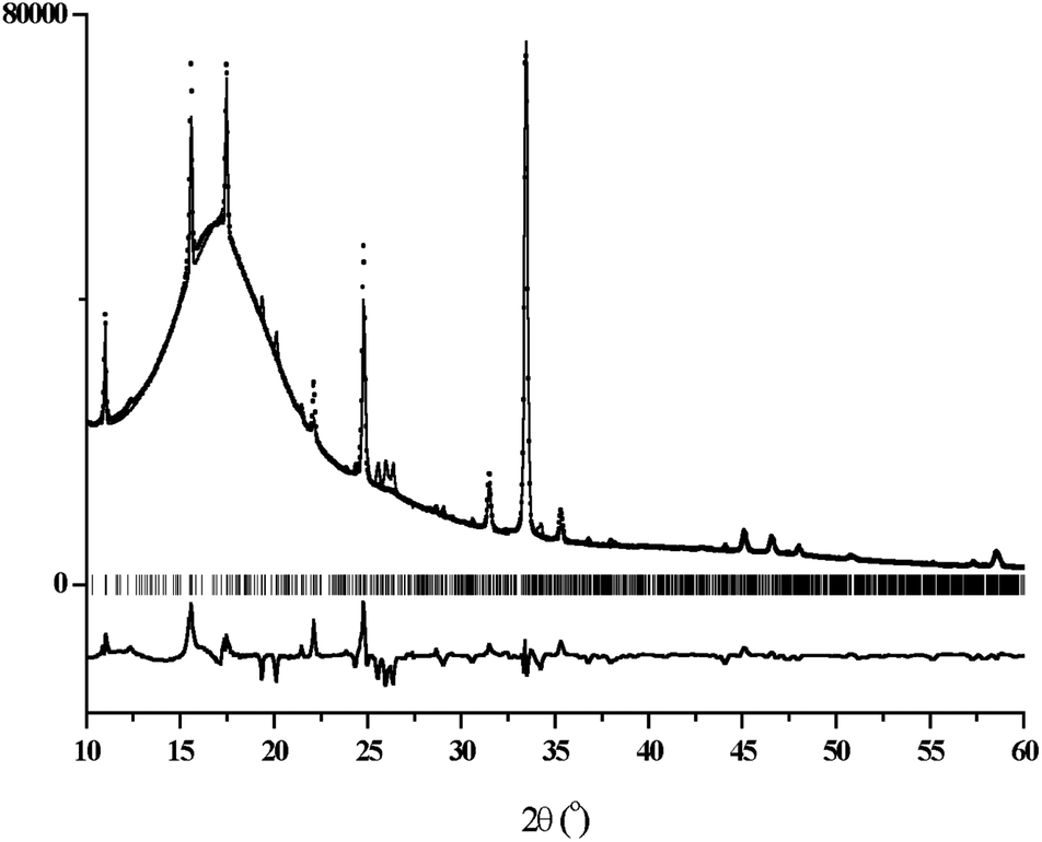 | ||
| Fig. 6 The final Rietveld plot for the X-ray diffraction pattern of BL film #1 (matrix polycarbonate) in the case of the TTF11I8 model structure. The experimental diffraction profile is indicated by black dots. The calculated diffraction profile is shown as the upper solid lines, the difference profile is shown as the bottom solid line and the vertical bars correspond to the calculated positions of the Bragg peaks. | ||
In Rietveld refinements, several directions of preferred orientation were tested, and remarkably better R-factors were obtained for two model structures, TTF11I8 and TTF7I5, when [010] was chosen as the direction of preferred orientation. In this choice for TTF11I8, the texture parameter r was refined to 0.39(2), and the maximum texture correction multiplier (∼16) for calculated F2(hkl) was applied to 0k0 reflections. It means, that most of coherently scattering regions of the conductive layer are oriented with the direction [010] perpendicular to the surface of the substrate, i.e. the ac plane of the unit cell of the TTF11I8 structure parallel to the substrate surface, while axis b is perpendicular (Fig. 7, left). In the case of the TTF7I5 model structure, when [010] was chosen as the direction of preferred orientation, the texture parameter r was refined to 0.44(2), revealing thus the same orientation of the conductive layer on the substrate surface (Fig. 7, right).
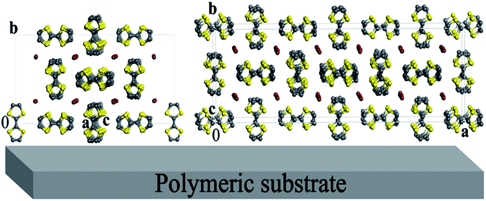 | ||
| Fig. 7 Idealized representation of a (TTF)I0.7+δ-based layer deposited on a polymeric substrate for the crystal structures TTF11I8 (left) and TTF7I5 (right). | ||
Therefore, all TTF stacks in the conducting (TTF)I0.7+δ layers of BL films are approximately parallel to the substrate surface. There are two types, A and B, of TTF stacks in the structures of TTF7I5 and TTF11I8 phases. In the A type the CC double bonds of TTFs are nearly parallel to the [100] direction in the TTF7I5 phase while for TTF11I8 are parallel to the [10−1] one.
By contrast, in type B TTF stacks, the CC double bonds are nearly parallel to the b axis in both structures. Accordingly with this observation, the conductivity in the A and B stacks should be one-dimensional because they both are parallel to the c axis in the TTF7I5 structure and to [101] in TTF11I8. Therefore, in an ideal case of one-domain of (TTF)I0.7+δ microcrystals we could observe strictly one-dimensional conductivity along the crystallographic directions [001] and [101] for TTF7I5 and TTF11I8, respectively.
3.8. Electromechanical properties of bilayer polymeric films with (TTF)I0.7+δ crystals
Two-contact resistance measurements of films #1, #2 and #3 show sheet resistances of 25–30, 6–8, and 16–20 kΩ □−1, respectively, suggesting that the number of continuous conducting paths extends uniformly through the (TTF)0.7+δ layers on the surfaces of BL films. The resistance of films #1–3 increased slightly with decreasing temperature in the high temperature range with temperature resistance coefficients for all films of 1.1%/deg in the temperature range between 28 and 55 °C (ESI, Fig. S4†). We also studied the responses of the films #1 and #2 to unidirectional stress tests to provide an overview of their mechanical and electromechanical properties. For this purpose their tensile tests were coupled with direct resistance measurements. The tensile tests (Fig. 8) showed that the mechanical characteristics of the BL films are similar. Indeed, the values of elastic limits (σyield) for films #1 and #2 were found to be 1.10% and 1.18%, respectively.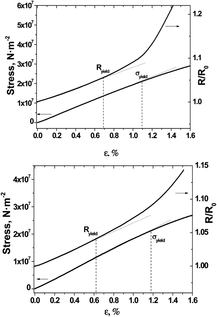 | ||
| Fig. 8 Stress–strain and resistance–strain curves for film #1 (top) and film #2 (bottom). Relative strain ε = (L − L0)100/L0, where L0 and L are the lengths of the film-based gauge without and under elongation, respectively. R/R0 is normalized resistance where R0 and R are resistances of the film-based gauge without and under elongation, respectively. | ||
Whereas, the Young's moduli (E), given by the slope of the stress–strain curve in the elastic region, were found to be 1.90 and 1.85 GPa for films #1 and #2, respectively. Taking into account that for a pristine (non-covered) polycarbonate film such parameters are σyield = 1.4% and E = 2.05 GPa,11 and for a cellulose triacetate film the Young's modulus is E = 2.06 GPa,35 the covering of polycarbonate and cellulose triacetate films with a layer of (TTF)I0.7+δ crystals does not adversely affect their mechanical characteristics. Fig. 8 also shows that resistance changes versus strain deviate from linear proportionality at relative strains (ε) of 0.7 and 0.6% for films #1 and #2, respectively. By analogy with the elastic limit point, this threshold limit can be termed as the resistance proportional limit of the BL film (Ryield).36 The nonlinearity observed for the resistance dependence on the strain above the threshold Ryield limit can be associated with the appearance of numerous nano-cracks formed perpendicularly to the elongation direction.36 Therefore, the Ryield values of BL films correspond to the elastic limit point of their polycrystalline conductive layers. The fact that the Ryield values for film #1 (0.70%) and film #2 (0.62%) are closely related to their values of σyield evidences the good robustness of both flexible BL films.
The experimental data presented in Fig. 8 additionally permitted us to plot the R(stress) dependence for BL films #1 and #2 (Fig. 9).
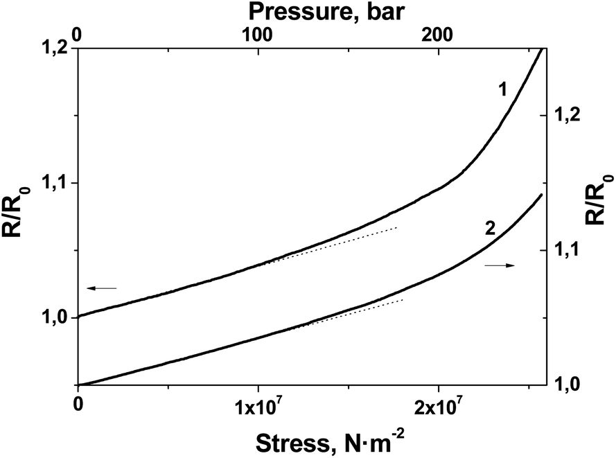 | ||
| Fig. 9 Normalized electrical resistance response of film #1 (curve 1) and #2 (curve 2) to monoaxial load. | ||
As Fig. 9 shows, in a range from 0 to 100 bar the electrical response linearly depends on stress; the sensitivity of the films to stress was calculated from the slope of the R(stress) dependence as 0.04%/bar and 0.035%/bar for film #1 and #2, respectively.
As shown in Fig. 10 and in the ESI (Fig. S5 and S6†), the electrical response of films to multi-cyclic monoaxial elongation, carried out in the elastic domain of deformation, is very reproducible and depends linearly on applied strain. The gauge factors, calculated as the ratio between the relative resistance change and the relative strain value, were found to be 7.7, 6.5 and 6.4 for films #1, #2 and #3, respectively. These values are very close to those reported for piezo-resistive BL films based on the α-(BEDT-TTF)2I3 molecular semimetal.7 As the gauge factor is controlled by the softness of the crystal structure of the organic molecular conductor, one may conclude that the structures of the 1-D organic conductor (TTF)I0.7+δ and 2-D organic conductor α-(BEDT-TTF)2I3 do not exhibit significant differences in their softness.
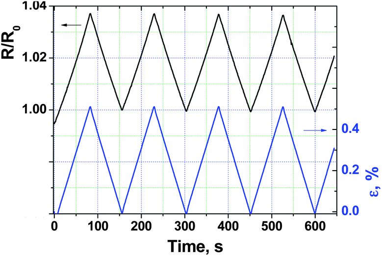 | ||
| Fig. 10 Normalized resistance response of the covering layer of film #1 (polycarbonate matrix) to cyclic elastic elongations with εmax = 0.5%. | ||
4. Summary and conclusions
Reaction conditions to obtain selectively crystals of the non-stoichiometric highly conducting (TTF)11I8 salt and the stoichiometric insulating (TTF)I3 one were found. Structurally the new modulated crystalline phase (TTF)11I8 is very similar to (TTF)7I5 and represents a new member of the non-stoichiometric (TTF)I0.7+δ family of salts.We used the oxidation of TTF with I2 to cover polymeric thin films of polycarbonate, cellulose triacetate, and cellulose acetate propionate with the oriented polycrystalline layer of molecular conductors (TTF)I0.70+δ making novel flexible piezoresistive BL thin films that exhibit similar electric transport and electromechanical properties. These novel BL materials offer new opportunities for engineering flexible all-organic sensing materials with advanced electromechanical properties.
Acknowledgements
The authors thank Xavier Fontrodona for his helpful discussion on the crystal structure. This work was supported in part by the Dirección General de Investigación, DGI, Spain (project CTQ2010-19501/BQU), the Generalitat de Catalunya (2009SGR00516), CIBER-BBN, an initiative funded by the VI National R&D&i Plan 2008–2011, Iniciativa Ingenio 2010, Consolider Program, CIBER Actions and financed by the Instituto de Salud Carlos III with assistance from the European Regional Development Fund, and Bilateral CSIC-Russia project (2010RU0038). The work was also supported by RFBR grants 11-03-93984 INIS-a and 12-03-12003ofi-m. E. Moreno-Calvo acknowledges the MICINN for a Juan de la Cierva postdoctoral contract and V. Lebedev acknowledges a grant FI-DGR from the Generalitat de Catalunya.Notes and references
- F. Axisa, P. M. Schmitt, C. Gehin, G. Delhomme, E. McAdams and A. Dittmar, IEEE Trans. Inform. Tech. Biomed., 2005, 9, 325 CrossRef.
- T. Someya, T. Sekitani, S. Iba, Y. Kato, H. Kawaguchi and T. Sakurai, Proc. Natl. Acad. Sci. U. S. A., 2004, 101, 9966 CrossRef CAS PubMed.
- F. Carpi and D. De Rossi, IEEE Trans. Inform. Tech. Biomed., 2005, 9, 574 CrossRef.
- J. K. Jeszka and A. Tracz, Polym. Adv. Technol., 1992, 3, 139–142 CrossRef CAS.
- E. E. Laukhina, V. A. Merzhanov, S. I. Pesotskii, A. G. Khomenko, E. B. Yagubskii, J. Ulanski, M. Kryszewski and J. K. Jeszka, Synth. Met., 1995, 70, 797 CrossRef CAS.
- G. Saito, in Organic Molecular Solids: Properties and Applications, CRC Press, 1997 Search PubMed.
- E. Laukhina, R. Pfattner, L. R. Ferreras, S. Galli, M. Mas-Torrent, N. Masciocchi, V. Laukhin, C. Rovira and J. Veciana, Adv. Mater., 2010, 22, 977 CrossRef CAS PubMed.
- H. Karimov, V. Laukhin, H. Ahmedov and E. Laukhina, SU1668855 A1, USSR, 1989.
- R. Kondo, M. Higa, S. Kagoshima, H. Hoshino, T. Mori and H. Mori, J. Phys. Soc. Jpn., 2006, 75, 044716 CrossRef.
- E. Laukhina, C. Rovira and J. Ulanski, Synth. Met., 2001, 121, 1407 CrossRef CAS.
- E. Laukhina, V. Lebedev, V. Laukhin, G. Oncins, R. Pfattner, C. Rovira and J. Veciana, in Solid-State Sensors, Actuators and Microsystems Conference (TRANSDUCERS), 2011 16th International, 2011, p. 1978 Search PubMed.
- R. Pfattner, V. Lebedev, B. Moradi, E. Laukhina, V. Laukhin, C. Rovira and J. Veciana, Sens. Transducers J., 2013, 17, 128 Search PubMed.
- V. Lebedev, E. Laukhina, C. Rovira, V. Laukhin and J. Veciana, in 26th European Conference on Solid-State Transducers, Eurosensor 2012, ed. R. Walczak and J. Dziuban, 2012, p. 603 Search PubMed.
- V. Laukhin, I. Sanchez, A. Moya, E. Laukhina, R. Martin, F. Ussa, C. Rovira, A. Guimera, R. Villa, J. Aguilo, J.-C. Pastor and J. Veciana, Sens. Actuators, A, 2011, 170, 36 CrossRef CAS PubMed.
- L. R. Ferreras, R. Pfattner, M. Mas-Torrent, E. Laukhina, L. Lopez, V. Laukhin, C. Rovira and J. Veciana, J. Mater. Chem., 2011, 21, 637 RSC.
- R. J. Warmack, T. A. Callcott and C. R. Watson, Phys. Rev. B: Solid State, 1975, 12, 3336 CrossRef CAS.
- R. B. Somoano, A. Gupta, V. Hadek, T. Datta, M. Jones, R. Deck and A. M. Hermann, J. Chem. Phys., 1975, 63, 4970 CrossRef CAS.
- B. A. Scott, S. J. Laplaca, J. B. Torrance, B. D. Silverman and B. Welber, J. Am. Chem. Soc., 1977, 99, 6631 CrossRef CAS.
- R. C. Teitelbaum, T. J. Marks and C. K. Johnson, J. Am. Chem. Soc., 1980, 102, 2986 CrossRef CAS.
- I. Smirani, R. Lipiec, A. Brau, J. P. Farges and A. Graja, J. Mater. Sci., 2001, 36, 1227 CrossRef CAS.
- L. Gomez and R. Rodriguez-Amaro, Langmuir, 2009, 25, 4799 CrossRef CAS PubMed.
- http://www.sigmaaldrich.com .
- F. D. Chattaway and G. Hoyle, J. Chem. Soc., 1923, 123, 654–662 RSC.
- Bruker, Advanced X-ray Solutions. SMART Version 5.631, 1997–2002 Search PubMed.
- Bruker, Advanced X-ray Solutions. SAINT +, Version 6.36A, 2001 Search PubMed.
- G. M. Sheldrick, Empirical Absorption Correction Program, Universität Göttingen, 1996 Search PubMed; Bruker, Advanced X-ray Solutions. SADABS Version 2.10, 2010 Search PubMed.
- G. M. Sheldrick, Program for Crystal Structure Refinement, Universität Göttingen, 1997 Search PubMed; Bruker, Advanced X-ray Solutions. SHELXTL Version 6.14, 2000–2003 Search PubMed.
- E. E. Laukhina, V. N. Laukhin, A. G. Khomenko and E. B. Yagubskii, Synth. Met., 1989, 32, 381 CrossRef CAS.
- C. K. Johnson and C. R. Watson, J. Chem. Phys., 1976, 64, 2271 CrossRef CAS , (Cif-files of TT F5I7 and TTF11I8 phases are THFULI01 and TTF11I8, respectively).
- T. C. Umland, S. Allie, T. Kuhlmann and P. Coppens, J. Phys. Chem., 1988, 92, 6456 CrossRef CAS.
- P. Deplano, J. R. Ferraro, M. L. Mercuri and E. F. Trogu, Coord. Chem. Rev., 1999, 188, 71 CrossRef CAS.
- R. Wojciechowski, J. Ulanski, M. Kryszewski, E. Laukhina and V. Tkacheva, Mol. Cryst. Liq. Cryst., 2001, 355, 351 CrossRef CAS.
- V. B. Zlokazov and V. V. Chernyshev, J. Appl. Crystallogr., 1992, 25, 447 CrossRef.
- W. A. Dollase, J. Appl. Crystallogr., 1986, 19, 267 CrossRef CAS.
- F. A. Akhmedov, B. I. Aikhodzhaev, G. S. Talipov and V. M. Surovkin, Polym. Mech., 1968, 4, 626 CrossRef.
- E. Laukhina, R. Pfattner, M. Mas-Torrent, C. Rovira, J. Veciana and V. Laukhin, Sens. Transducers J., 2011, 1 CAS.
Footnote |
| † Electronic supplementary information (ESI) available: Scheme of the preparation of BL films 1–3 and their X-ray diffraction patterns; photograph of the single crystals of TTF11I8 and (TTF)I3; temperature dependence of the normalized electrical resistance of BL films 1–3; electrical resistance response of BL films to cyclic elastic elongation. CCDC 949070. For ESI and crystallographic data in CIF or other electronic format see DOI: 10.1039/c3tc31513d |
| This journal is © The Royal Society of Chemistry 2014 |