Transparent conducting oxide top contacts for organic electronics†
Joseph B.
Franklin
,
James B.
Gilchrist
,
Jonathan M.
Downing‡
,
Kirsty A.
Roy
and
Martyn A.
McLachlan
*
Department of Materials & Centre for Plastic Electronics, Imperial College London, UK. E-mail: martyn.mclachlan@imperial.ac.uk; Fax: +44 (0)207594 6757; Tel: +44 (0)207594 9692
First published on 22nd October 2013
Abstract
A versatile method for the deposition of transparent conducting oxide (TCO) layers directly onto conjugated polymer thin film substrates is presented. Using pulsed laser deposition (PLD) we identify a narrow window of growth conditions that permit the deposition of highly transparent, low sheet resistance aluminium-doped zinc oxide (AZO) without degradation of the polymer film. Deposition on conjugated polymers mandates the use of low growth temperatures (<200 °C), here we deposit AZO onto poly-3-hexylthiophene (P3HT) thin films at 150 °C, and investigate the microstructural and electrical properties of the AZO as the oxygen pressure in the PLD chamber is varied (5–75 mTorr). The low oxygen pressure conditions previously optimized for AZO deposition on rigid substrates are shown to be unsuitable, resulting in catastrophic damage of the polymer films. By increasing the oxygen pressure, thus reducing the energy of the ablated species, we identify conditions that allow direct deposition of continuous, transparent AZO films without P3HT degradation. We find that uptake of oxygen into the AZO films reduces the intrinsic charge carriers and AZO films with a measured sheet resistance of approximately 500 Ω □−1 can be prepared. To significantly reduce this value we identify a novel process in which AZO is deposited over a range of oxygen pressures – enabling the deposition of highly transparent AZO with sheet resistances below 50 Ω □−1 directly onto P3HT. We propose these low resistivity films are widely applicable as transparent top-contacts in a range of optoelectronic devices and highlight this by demonstrating the operation of a semi-transparent photovoltaic device.
Introduction
Transparent conducting oxides (TCOs) are ubiquitous in optoelectronic devices,1 including display technologies, solar cells and light emitting diodes.2 The drive towards flexible and lightweight technologies has stimulated research aimed at identifying transparent conductors compatible with flexible substrates.3 Proposed alternative transparent conductors include nanowires,4 carbon nanotubes5 and more recently graphene.6 The motivation for studying such alternatives is often based on processability rather than performance, hence metal oxide based transparent conductors are still preferred owing to their superior stability, uniformity and performance. There have been a limited number of reports on the deposition of undoped ZnO onto functional organic substrates7,8 however such films have exhibited low crystallinity, due to constraints on deposition conditions and to date there have been no detailed examples describing the direct deposition of highly conducting TCOs. When considering TCOs, the deposition of low sheet resistance (Rs < 100 Ω □−1) electrodes has been demonstrated on robust polymer substrates,9 such as PET, primarily using sputtering techniques.10 Although sputter damage occurs on such substrates11 their role is mechanical as opposed to functional, therefore this interfacial degradation is deemed acceptable. To date, there have been no detailed examples outlining the direct deposition of highly conducting TCOs directly onto functional organic substrates. For many organic optoelectronic devices, the polymer active layer thickness is often <200 nm and as a result, the penetration of sputtered particles would compromise the integrity of the polymer/TCO interface. Owing to the sensitivity of functional polymer materials to air, humidity12 and elevated temperature,13 limitations are placed on many solution based techniques and processes. Consequently, the majority of organic optoelectronic devices fabricated today are prepared bottom-up, with the TCO deposited early in the process onto a transparent substrate. For many device applications, this architecture places constraints on the processing of the active layers and results in adverse reactions e.g. degradation at metal–organic interfaces.14 The ability to directly deposit a TCO as a top contact is desirable as it enables device fabrication using metallic bottom contacts and introduces the possibility of TCOs acting as an encapsulant to protect the organic active layers from UV, moisture and oxygen.12Zinc oxide (ZnO) has been extensively studied as a TCO owing to its high electron mobility,15 excellent transparency16 and ease of processing.17 Using pulsed laser deposition (PLD), it is possible to deposit undoped ZnO films with relatively low resistivity (10−1–10−2 Ω cm);18,19 the intrinsic carrier concentration is closely linked to the oxygen pressure during growth.19,20 However, intrinsically doped ZnO is generally unsuitable for use in TCO applications owing to its instability in different working environments.21 Doping ZnO with group III elements decreases the resistivity (10−3–10−4 Ω cm), reduces instability and supports the formation of highly transparent >85% films.22,23 AZO is particularly attractive as a TCO as thin films have been reported with sheet resistance and transparency values rivalling the most commonly used TCO, tin-doped indium oxide (ITO),23–26 but with lower material and processing costs.3 The current challenge is to prepare similar high quality AZO at low temperature and under deposition conditions that will not degrade functional polymer layers.
Building on our recent demonstration of PLD as a technique for depositing semiconducting metal oxides at low temperatures onto functional polymer substrates,27 we consider PLD for the deposition of TCOs. Herein we demonstrate the deposition of highly transparent, low resistivity, highly crystalline AZO electrodes directly onto functional polymer thin films and identify the deposition conditions that enable such processing. We correlate the morphological, crystallographic and electrical properties of the AZO films with the deposition oxygen pressure and probe the polymer–TCO interface of multilayer films.
Deposition of AZO on polymer substrates
To determine the optimum Al dopant concentration, films were deposited (50 mTorr) from targets containing 1.0, 1.5, 2.0, 2.5, 3.0 and 3.5 wt% Al2O3. The minimum measured Rs was at 2.5 wt% Al2O3 (ESI, Fig. S1†). The 2.5 wt% addition resulted in an Rs reduction of over 2 orders of magnitude compared with un-doped ZnO, this target composition was used for all subsequent film growth. AZO films were deposited directly onto 50 nm P3HT films on glass substrates and simultaneously on bare glass substrates at a substrate temperature (Ts) of 150 °C over the background oxygen pressure (Pd) range of 5–75 mTorr. SEM micrographs of films deposited at 5 mTorr (Fig. 1a) show large cracks and film delamination across the substrate. Furthermore the characteristic red/purple colour of P3HT was completely absent across the entire substrate following deposition, suggesting the high-energy ablated species has sputtered the polymer from the substrate. As the Pd is increased over the range 25–45 mTorr the cracking and damage is significantly reduced (Fig. 1b–e) however cracking is not eliminated until Pd is increased to 50 mTorr (Fig. 1f). Films deposited at >50 mTorr are continuous across the entire substrate (Fig. 2a) and exhibit the anticipated columnar grain structure (Fig. 2b). The macroscopic damage to the films deposited at Pd < 25 mTorr prevented accurate thickness measurements being obtained, while those deposited at 25 < Pd < 75 mTorr had measured thicknesses ranging from 620–680 nm (10![[thin space (1/6-em)]](https://www.rsc.org/images/entities/char_2009.gif) 000 pulses) corresponding to growth rates between 0.49 and 0.54 nm s−1.
000 pulses) corresponding to growth rates between 0.49 and 0.54 nm s−1.
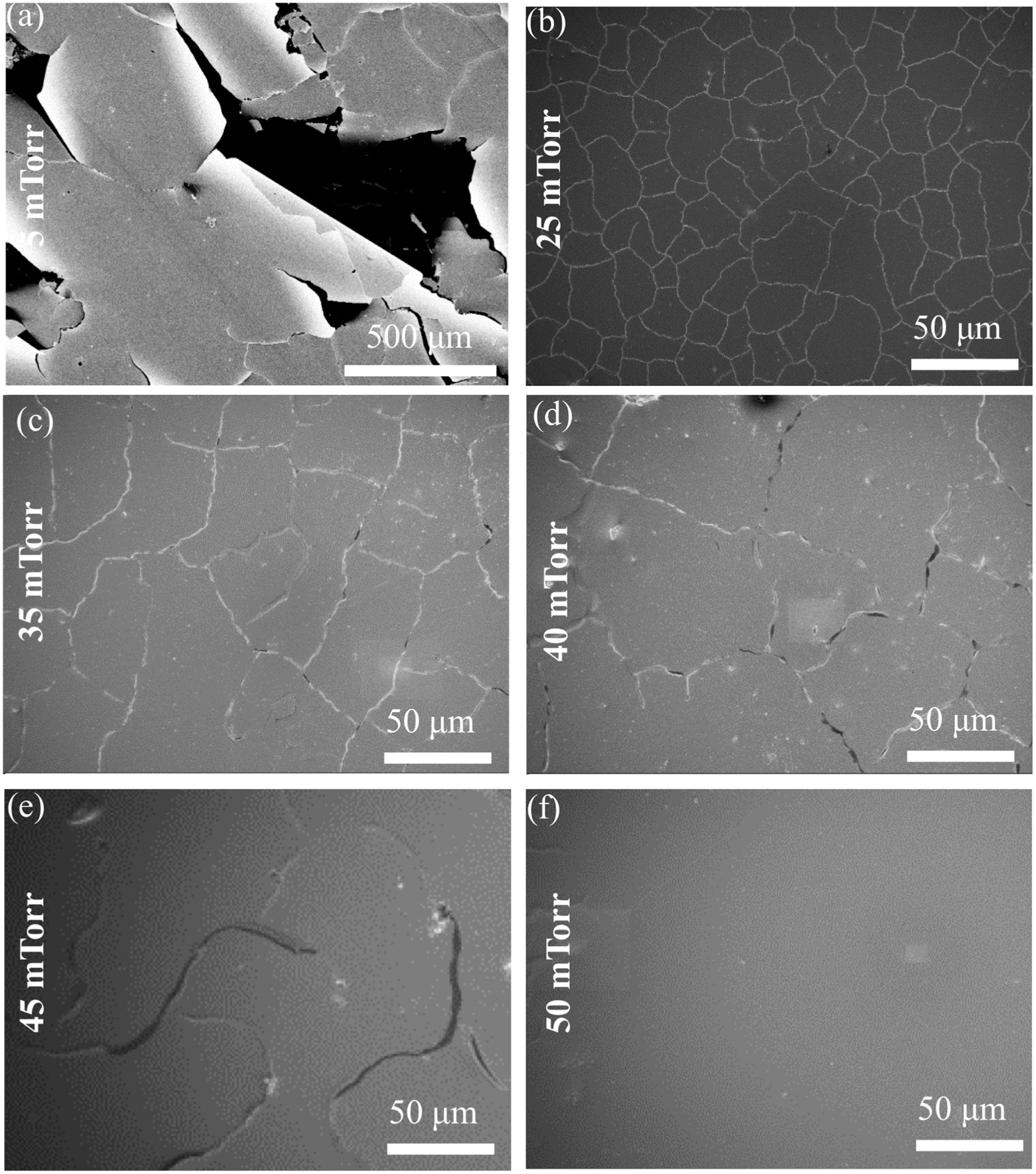 | ||
| Fig. 1 SEM micrographs showing surface images of AZO films deposited directly onto 50 nm poly(3-hexylthiophene) (P3HT) coated glass substrates, (a) evidence of macroscopic damage caused by high energy incident species on the polymer substrate is evident, (b–e) increased oxygen pressure significantly reduces the extent of damage although microscopic cracking is still observed, (f) at an oxygen pressure of 50 mTorr cracking is eliminated. | ||
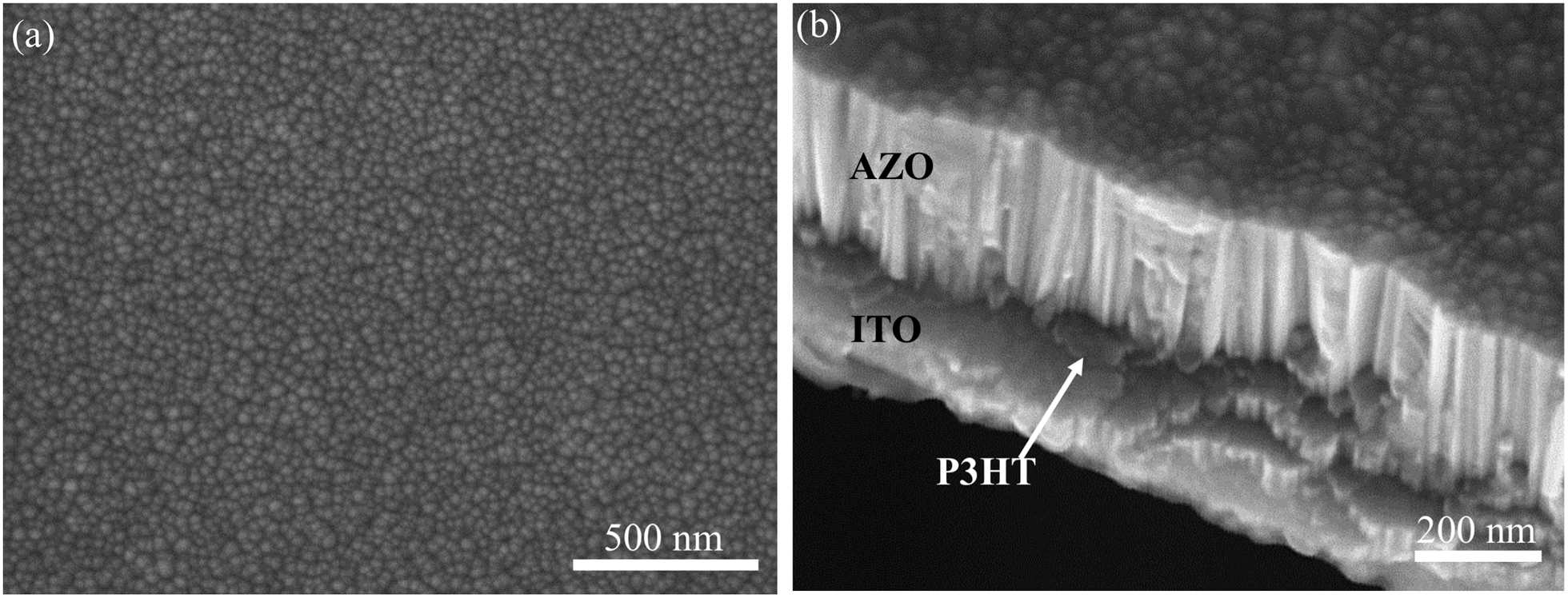 | ||
| Fig. 2 SEM micrographs showing (a) surface and (b) cross sectional view of AZO film deposited onto P3HT coated substrate at an oxygen pressure of 75 mTorr. From the cross sectional image the hexagonal columnar nature of the AZO can be observed in addition to the underlying polymer layer (images are typical for films prepared ≥50 mTorr). | ||
XRD data for an AZO film deposited at 75 mTorr (Ts = 150 °C) is shown (Fig. 3a), the data is typical of all films deposited >50 mTorr. Single-phase ZnO is confirmed with the (0002) and (0004) diffraction peaks observed at 34.4 and 72.3 °2θ respectively. No secondary phases such as Al2O3 or Al are detected, confirming successful incorporation of Al into the growing ZnO films. The influence of Pd is evident on the (0002) diffraction peak, which shifts to higher °2θ as the pressure is increased (Fig. 3b). This indicates a reduction in the c-axis lattice parameter i.e. the oxygen content of the films is increased as Pd increases.28,29 Strain induced by oxygen deficiency30,31 may also contribute to the cracking observed at <50 mTorr (Fig. 1 a–e). The peak position stabilizes (at 34.55 °2θ) when Pd ≥ 50 mTorr, signifying that the ablated species in the plume have fully interacted with the background gas. Despite the reduction in energy caused by this interaction, which increases with Pd, highly crystalline AZO can consistently be prepared at only 150 °C.
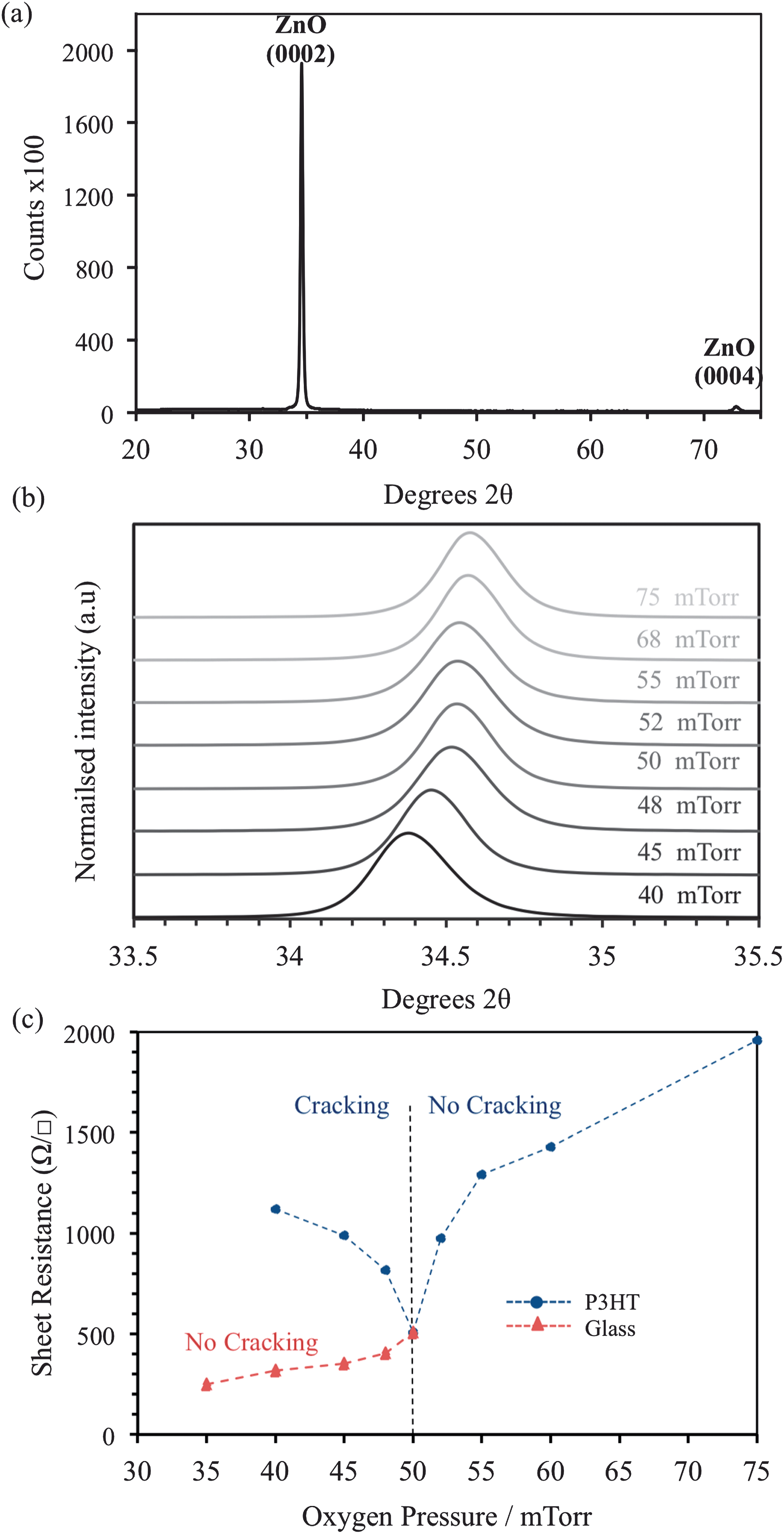 | ||
| Fig. 3 (a) X-ray diffraction pattern of AZO film deposited on P3HT at 75 mTorr, peaks are indexed to undoped ZnO, (b) offset diffraction data showing the shift in the (0002) peak as oxygen pressure is varied, and (c) measured sheet resistance of AZO deposited on glass and P3HT, significant differences in behaviour are observed at oxygen pressures <50 mTorr attributed to cracking in films deposited on P3HT at lower Pd. | ||
Sheet resistance measurements
Sheet resistance (Rs) measurements were obtained for the AZO films deposited at Pd of 35–75 mTorr using a 4-point probe. The severe cracking and delamination of the films grown <25 mTorr on P3HT prevented Rs measurements. The Rs values for films deposited on bare glass and P3HT substrates at 35 ≤ Pd ≤ 75 mTorr are shown in Fig. 3c. As Pd is reduced from 75–50 mTorr identical Rs values are obtained on each substrate. However, at Pd < 50 mTorr the Rs values differ significantly depending on the substrate. On P3HT, a minimum Rs of 509 Ω □−1 was measured at Pd = 50 mTorr, which increases as Pd decreases, this is attributed to the formation of the macroscopic cracks, the severity increases with decreasing Pd (Fig. 1). On glass substrates, no cracking is observed at Pd < 50 mTorr and the Rs continues to reduce, reaching a minimum of 17 Ω □−1 at 5 mTorr. The increase in Rs at elevated Pd can be attributed to increased oxygen incorporation in the growing films. On glass the reduction of Rs at low Pd is anticipated as the concentration of intrinsic defects increases under these conditions. The similarity in Rs values above 50 mTorr is not coincidental, the electronic properties of the AZO and the observed damage to the P3HT film are both influenced by the interaction of the ablated species with the background gas. It is thought that at Pd = 50 mTorr the majority species in the plume become thermalized, owing to multiple collisions with molecular oxygen,27,32 leaving a narrow window of Pd in which the intrinsic conductivity can be controlled whilst maintaining the integrity of the underlying substrate.Variable pressure AZO deposition
To reduce the Rs values of AZO deposited on P3HT, whilst preserving the integrity of the polymer, Pd in the chamber was varied during deposition. In order to protect the polymer from damage from high-energy species (at low pressure), a thin AZO layer was first deposited at Pd > 50 mTorr, after which the Pd was reduced. In the preliminary experiments, the initial layer was deposited at 50 mTorr with either 1000 or 2500 pulses (thickness = 70 or 190 nm) then Pd was reduced to 10–25 mTorr. Under these conditions severe cracking of the AZO occurred, however unlike the cracking described in the previous section, its origin is not due to damage of the P3HT, but rather, due to strain in the AZO. XRD data, Fig. 4a, shows a large shift in (0002) peak position for a multilayer film deposited initially at 50 mTorr then 25 mTorr (34.20 °2θ) compared with AZO deposited on glass at 25 mTorr (34.30 °2θ).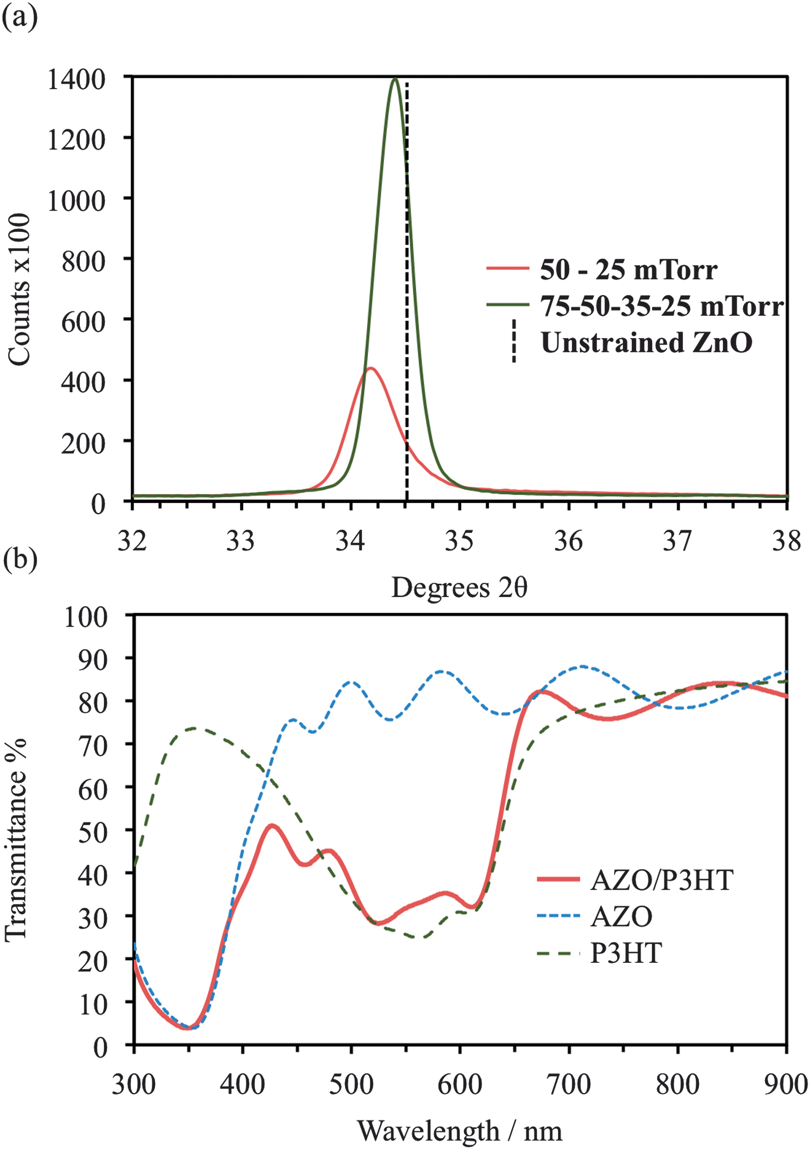 | ||
| Fig. 4 (a) X-ray diffraction patterns showing the (0002) diffraction peak shift caused by strain accumulation in AZO films deposited at different oxygen pressures. Strain is reduced by increasing the number of oxygen pressures used during deposition (vertical line indicates peak position of unstrained lattice) (see Fig. 3b), (b) UV-vis spectra of P3HT, AZO on glass and AZO on P3HT (all AZO deposited at 75–50 to 35–25 mTorr). The interference fringes observed in the AZO films are indicative of sharp interfaces between the layers. | ||
To eliminate the cracking, deposition was carried out with incremental reductions of Pd (75, 50, 35 & 25 mTorr, 2500 pulses each); the measured (0002) peak position was 34.4 °2θ, close to that of unstrained ZnO (Fig. 3a). The resultant 600 nm thick films were continuous across the substrate area with a measured Rs of 46.2 Ω □−1 (2.8 × 10⁻³ Ω cm). UV-vis spectroscopy (Fig. 4b) confirms the deposited films are highly transparent and the absorption bands of the P3HT confirm the molecular ordering of the polymer has not been disrupted by the AZO deposition.33 The fringes in the absorption spectra indicate a sharp interface between the AZO and the glass, these are also observed for the AZO on P3HT films (Fig. 4b) confirming no degradation has occurred at this interface. To demonstrate the flexibility of the deposition process AZO was deposited using this variable pressure method, specifically at 75–50 to 35–25 mTorr (1000 pulses each) onto a photovoltaic-like multilayer consisting glass/ITO/PEDOT:PSS/P3HT:PCBM. The resultant cross sectional TEM micrograph, Fig. 5a, shows a clear, sharp interface between P3HT:PCBM and the AZO. Significantly, the interface between the PEDOT:PSS/P3HT:PCBM can also be easily observed, the lower intensity arising from the increase in density of the PEDOT:PSS. Both sharp interfaces suggest that no intermixing or disordering has occurred during the thermal processing associated with PLD. Fig. 5b shows a high magnification TEM image of the AZO/P3HT:PCBM interface, the highly crystalline nature of the AZO is evident with (0002) lattice fringes highlighted perpendicular to the blend surface. The calculated (0002) lattice spacing is consistent with those calculated from the XRD data.
 | ||
| Fig. 5 (a) TEM micrograph showing in cross-section a multilayer structure consisting glass/ITO/PEDOT:PSS/P3HT:PCBM/AZO (AZO deposited at 75–50 to 35–25 mTorr). The well preserved interface between the AZO and P3HT:PCBM is clearly seen, suggesting no damage has occurred during AZO deposition. Importantly the interface between the PEDOT; PSS/P3HT:PCBM can also be observed signifying no degradation or intermixing has occurred during the low temperature PLD processing, (b) high magnification TEM image showing the organic:AZO interfacial region, the (0002) lattice fringes are highlighted. | ||
Device data
Photovoltaic devices were constructed to give a layer structure similar to that shown in Fig. 5a. AZO top contacts were deposited at 75/50/35/25 mTorr, giving a resultant device configuration of ITO/PEDOTPSS/P3HT:PCBM/AZO. The current density–voltage (J–V) scans under dark and illumination are shown in Fig. 6. The dark curves typically exhibit clear rectification (image inset), indicating the formation of a functional device stack not degraded by AZO deposition. Under illumination, the short-circuit current (Jsc), open-circuit voltage (Voc) and resulting power conversion efficiency (PCE) were 5.67 mAcm−2, 390 mV and 0.51% respectively.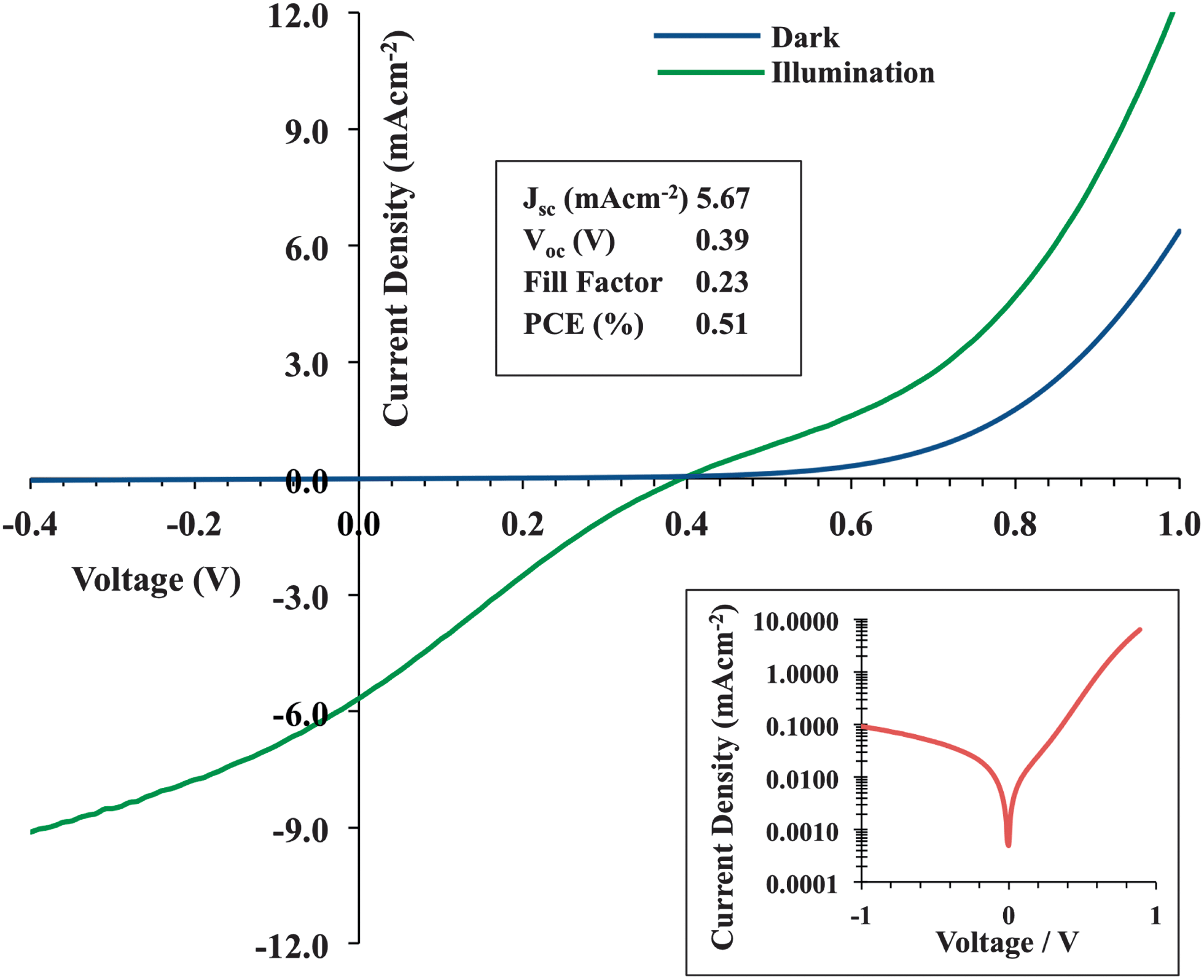 | ||
| Fig. 6 Current density–voltage (J–V) plot for a semi-transparent organic solar cell ITO/PEDOT:PSS/P3HT/PCBM/AZO with measured parameters indicated. Inset shows clear rectification behaviour in the dark. | ||
Deposition by PLD on to organic films necessitates the use of moderate temperatures. Here substrate heating was combined with the necessary thermal annealing of the active layer whereby heating to 150 °C for 25 minutes occurred during AZO deposition.34 The formation of optimised BHJ morphologies is extremely sensitive to processing conditions,35 whereby over-aging of the structure leads to inefficient devices as a result of morphological coarsening.36,37 Control devices annealed under the same conditions with Al top-contacts showed similar s-shaped curves (ESI, Fig. S2†). Owing to the rectification observed in the dark scans we speculate that it is the annealing which leads to an unfavourable active layer morphology and the AZO deposit is not degrading the organic components.
Conclusions
We have demonstrated the deposition of highly transparent, low sheet resistance and crystalline AZO films directly onto conjugated polymer thin films. We have established that the oxygen pressure in the PLD chamber plays an essential role in (i) protecting the polymer from damage induced by ablated species, and (ii) influencing the electrical properties of the AZO. Deposition at a fixed oxygen pressure, 50 mTorr, produces highly transparent and crack free AZO on P3HT with a sheet resistance of ∼500 Ω □−1. Although further reduction of the oxygen pressure is shown to reduce the sheet resistance on glass substrates, this results in catastrophic damage to the polymer substrates, as high-energy species from the plume damaging the organic film. To reduce the sheet resistance of the AZO and compensate for strain-induced delamination, films were deposited at successively lower oxygen pressures; stepped from 75–50 to 35–25 mTorr resulting in AZO films on P3HT with a measured sheet resistance of 46.2 Ω □−1 (2.8 × 10⁻³ Ω cm). To highlight the versatility of the method we have demonstrated a semi-transparent photovoltaic device with an AZO top contact. This work highlights the applicability of directly depositing TCOs onto functional soft materials and offers stimulating possibilities for the growth of organic optoelectronic devices, presenting opportunities for new device architectures and assemblies i.e. metal electrode upwards or the possibility of utilising TCOs for device encapsulation.Experimental
AZO targets were prepared by adding 2.5 wt% Al2O3 powder (99.9%) to ZnO powder (99.999%), both <50 nm particle size (Sigma Aldrich) and ball milled for 24 hours. The homogeneous product was uniaxially pressed (10 kN) and sintered in air at 1000 °C for 10 hours.Substrates (12 × 12 mm) were cleaned by sequential ultrasonic washing in acetone, isopropanol and de-ionized water and dried under a N2 flow. Poly-3-hexylthiophene (P3HT) (Merck regioregular Mw = 60 kg mol−1) in chlorobenzene (12.5 mg ml−1) was spin coated onto heated (150 °C) glass substrates. In the multilayer polymer films, poly(3,4-ethylenedioxythiophene) poly(styrenesulfonate) (PEDOT:PSS) (Clevios 4083 Liquid Formulation) was spin-coated at room temperature and dried at 120 °C prior to P3HT deposition. To prepare device-like structures phenyl-C61-butyric acid methyl ester (PCBM, Solenne) was mixed with P3HT in chlorobenzene in a ratio of 1:1 (15 mg ml−1 of each).
For AZO deposition, substrates were fixed to a resistive heater using silver paint and heated to 150 °C. Temperature was controlled to ±0.5 °C by a Eurotherm unit attached to a thermocouple embedded within the heating block. A base pressure of 3 × 10⁻⁵ Torr (4 × 10⁻³ Pa) was maintained and the background oxygen pressure (Pd) was varied between 5 and 75 mTorr (0.667–10.005 Pa). A KrF laser (248 nm) was used with a pulse duration and laser frequency set at 25 ns and 8 Hz respectively. The resulting energy of the beam in the chamber was measured to be 400 mJ and was focused on an area of 0.16 cm2 on the target surface (2.5 J cm−2). The targets were held at a fixed distance (50 mm) from the substrate surface and the target surface pre-ablated to remove any surface impurities. The substrates were then exposed and the target was subjected to 5000 or 10000 pulses. After deposition the chamber was backfilled with oxygen (600 mTorr) and the samples were cooled to room temperature.
Film morphology was assessed using a LEO Gemini 1525 field emission scanning electron microscope (FE-SEM), operating at 5 kV. TEM cross-sections were prepared using a FEI Helios dual-beam system, with the final thinning performed at 1 kV. TEM images were obtained (Fig. 5a) using a JEOL 2010 operated at 200 kV and (Fig. 5b) an FEI Titan 80–300 with a Cs corrector operated at 300 kV. The average (n = 97) fringe spacing was measured using the line-profile tool in Gatan's Digital Micrograph software. XRD measurements were performed with a PANalytical X'Pert pro MPD diffractometer equipped with an X'celerator detector using CuKα radiation (λ = 1.5418 Å), operating at 40 kV and 40 mA. UV-vis spectroscopy was carried out using a monochromated white light source (300–900 nm) attached to a custom optical bench, controlled by BenWin + software. Thickness measurements were made using a Dektak 150 stylus profilometer with a working accuracy of 0.6 nm (measurements averaged over 5 scans). The J–V characteristics were obtained using an Oriel solar simulator under a xenon lamp with AM1.5G filters and 100 mW cm−2 (1 sun) illumination.
Acknowledgements
The authors are grateful to Sebastian Wood (IC Physics) for his assistance in preparing the polymer substrates. JBF is grateful to KAUST for research funding through the Imperial College Academic Excellence Alliance. JD was supported through the ESPRC first-grant scheme EP/F056362/1.Notes and references
- D. S. Ginley and C. Bright, MRS Bull., 2000, 25, 4 CrossRef.
- H. Liu, V. Avrutin, N. Izyumskaya, U. Ozgur and H. Morkoc, Superlattices Microstruct., 2010, 48, 458–484 CrossRef CAS PubMed.
- S. Logothetidis, Mater. Sci. Eng., B, 2008, 152, 96–104 CrossRef CAS PubMed.
- A. R. Rathmell, S. M. Bergin, Y.-L. Hua, Z.-Y. Li and B. J. Wiley, Adv. Mater., 2010, 22, 3558–3563 CrossRef CAS PubMed.
- R. V. Salvatierra, C. E. Cava, L. S. Roman and A. J. G. Zarbin, Adv. Funct. Mater., 2013, 23, 1490–1499 CrossRef CAS.
- J. Wu, H. A. Becerril, Z. Bao, Z. Liu, Y. Chen and P. Peumans, Appl. Phys. Lett., 2008, 92, 263302 CrossRef.
- J. Gilot, I. Barbu, M. M. Wienk and R. A. J. Janssen, Appl. Phys. Lett., 2007, 91, 113520 CrossRef.
- Y. Jouane, S. Colis, G. Schmerber, P. Kern, A. Dinia, T. Heiser and Y. A. Chapuis, J. Mater. Chem., 2011, 21, 1953–1958 RSC.
- H. Kim, J. S. Horwitz, G. P. Kushto, Z. H. Kafafi and D. B. Chrisey, Appl. Phys. Lett., 2001, 79, 284–286 CrossRef CAS.
- T. Minami, H. Sonohara, T. Kakumu and S. Takata, Thin Solid Films, 1995, 270, 37–42 CrossRef CAS.
- C. Koidis, S. Logothetidis, D. Georgiou, A. Laskarakis, S. Lousinian, I. Tsiaoussis and N. Frangis, Phys. Status Solidi A, 2008, 205, 1988–1992 CrossRef CAS.
- H. Hintz, H. J. Egelhaaf, L. Lüer, J. Hauch, H. Peisert and T. Chassé, Chem. Mater., 2010, 23, 145–154 CrossRef.
- C. H. Peters, I. T. Sachs-Quintana, J. P. Kastrop, S. Beaupré, M. Leclerc and M. D. McGehee, Adv. Energy Mater., 2011, 1, 491–494 CrossRef CAS.
- M. T. Lloyd, D. C. Olson, P. Lu, E. Fang, D. L. Moore, M. S. White, M. O. Reese, D. S. Ginley and J. W. P. Hsu, J. Mater. Chem., 2009, 19, 7638–7642 RSC.
- E. M. Kaidashev, M. Lorenz, H. v. Wenckstern, A. Rahm, H.-C. Semmelhack, K.-H. Han, G. Benndorf, C. Bundesmann, H. Hochmuth and M. Grundmann, Appl. Phys. Lett., 2003, 82, 3901–3903 CrossRef CAS.
- T. Minami, H. Nanto and S. Takata, Appl. Phys. Lett., 1982, 41, 958–960 CrossRef CAS.
- M. N. Kamalasanan and S. Chandra, Thin Solid Films, 1996, 288, 112–115 CrossRef CAS.
- A. N. Banerjee, C. K. Ghosh, K. K. Chattopadhyay, H. Minoura, A. K. Sarkar, A. Akiba, A. Kamiya and T. Endo, Thin Solid Films, 2006, 496, 112–116 CrossRef CAS PubMed.
- K. Ellmer, A. Klein and B. Rech, Transparent Conductive Zinc Oxide Basics and Applications in Thin Film Solar Cells, Springer, 2008 Search PubMed.
- C. Jagadish and S. Pearton, Zinc Oxide Bulk, Thin Films and Nanostructures, Elsevier, 2006 Search PubMed.
- T. Minami, H. Nanto, S. Shooji and S. Takata, Thin Solid Films, 1984, 111, 167–174 CrossRef CAS.
- H. Kim, C. M. Gilmore, J. S. Horwitz, A. Pique, H. Murata, G. P. Kushto, R. Schlaf, Z. H. Kafafi and D. B. Chrisey, Appl. Phys. Lett., 2000, 76, 259–261 CrossRef CAS.
- H. Agura, A. Suzuki, T. Matsushita, T. Aoki and M. Okuda, Thin Solid Films, 2003, 445, 263–267 CrossRef CAS.
- T. Ohshima, Y. Murakami, H. Kawasaki, Y. Suda and Y. Yagyu, Jpn. J. Appl. Phys., 2011, 50 Search PubMed.
- B. Thestrup and J. Schou, Appl. Phys. A, 1999, 69, S807–S810 CrossRef CAS.
- K. Ellmer and R. Mientus, Thin Solid Films, 2008, 516, 4620–4627 CrossRef CAS PubMed.
- J. B. Franklin, J. M. Downing, F. Giuliani, M. P. Ryan and M. A. McLachlan, Adv. Energy Mater., 2012, 5, 528–531 CrossRef.
- J. B. Franklin, B. Zou, P. Petrov, D. W. McComb, M. P. Ryan and M. A. McLachlan, J. Mater. Chem., 2011, 21, 8178–8182 RSC.
- S. Choopun, R. D. Vispute, W. Noch, A. Balsamo, R. P. Sharma, T. Venkatesan, A. Iliadis and D. C. Look, Appl. Phys. Lett., 1999, 75, 3947–3949 CrossRef CAS.
- S. S. Kim and B.-T. Lee, Thin Solid Films, 2004, 446, 307–312 CrossRef CAS PubMed.
- X. Chen, W. Guan, G. Fang and X. Z. Zhao, Appl. Surf. Sci., 2005, 252, 1561–1567 CrossRef CAS PubMed.
- D. B. Geohegan and A. A. Puretzky, Appl. Surf. Sci., 1996, 96–98, 131–138 CrossRef CAS.
- V. Shrotriya, J. Ouyang, R. J. Tseng, G. Li and Y. Yang, Chem. Phys. Lett., 2005, 411, 138–143 CrossRef CAS PubMed.
- M. T. Dang, L. Hirsch and G. Wantz, Adv. Mater., 2011, 23, 3597–3602 CrossRef CAS.
- C. Müller, T. A. M. Ferenczi, M. Campoy-Quiles, J. M. Frost, D. D. C. Bradley, P. Smith, N. Stingelin-Stutzmann and J. Nelson, Adv. Mater., 2008, 20, 3510–3515 CrossRef.
- G. Li, V. Shrotriya, J. Huang, Y. Yao, T. Moriarty, K. Emery and Y. Yang, Nat. Mater., 2005, 4, 864–868 CrossRef CAS.
- X. Yang, J. Loos, S. C. Veenstra, W. J. H. Verhees, M. M. Wienk, J. M. Kroon, M. A. J. Michels and R. A. J. Janssen, Nano Lett., 2005, 5, 579–583 CrossRef CAS PubMed.
Footnotes |
| † Electronic supplementary information (ESI) available. See DOI: 10.1039/c3tc31296h |
| ‡ Current address: Materials Science and Engineering Laboratory, National Institute of Standards and Technology, Gaithersburg, Maryland 20899-8541, USA. |
| This journal is © The Royal Society of Chemistry 2014 |