
A successive photocurrent transient study to probe the sub-band gap electron and hole traps in ZnO nanorods
Dipanwita Sett,
Sanjit Sarkar and
Durga Basak*
Department of Solid State Physics, Indian Association for the Cultivation of Science, Jadavpur, Kolkata 700032, India. E-mail: sspdb@iacs.res.in
First published on 24th October 2014
Abstract
Though persistent photoconductivity and spectral response characteristics corresponding to sub-band gap energies of ZnO as a result of different defects are certainly problematic, study on this is quite useful in the sense that it provides information about the defects levels. A developed understanding of the energetic distributions of sub-band gap electron and hole traps in ZnO nanorods is pre-requisite for device applications and needs to be acquired. Through a study on the simple successive photocurrent transients of as-grown and annealed aqueous chemically grown ZnO nanorods, we have revealed the sub-band gap electron and hole traps responsible for their visible photoresponse. The evolutions in the room temperature photoluminescence properties of ZnO nanorods with annealing temperature have also been investigated critically to correlate the corresponding photocurrent results. As-grown samples show fewer excess O related electron trap states with energy corresponds to (Ec − 1.77 eV). A greater amount of O vacancy related hole traps, as well as fewer O interstitial related electron traps with energy corresponds to (Ec − 2.34 eV) were detected in the as-grown as compared to the annealed samples. These findings also provide general guidelines for probing sub-band gap traps, and engineering the optoelectronic properties of similar oxide semiconducting nanoparticles.
Introduction
Recent progress in the synthesis and characterization of nanosized ZnO particles has been driven by their potential application in fabricating nanoscale optoelectronic and electronic devices, such as short wavelength light emitting and laser diodes, UV photodetectors, solar cells and transistors,1–8 due to their wide and direct band gap of 3.37 eV, large exciton binding energy of 60 meV, high electron mobility, low cost synthesis, and ability to be etched by chemical techniques as compared to other II–VI semiconductors. However, unlike many topics in the field of oxide semiconductors, it seems there is a tangled web of research and opinions when it comes to the properties of ZnO and its defects. Therefore, an understanding of the sub-band gap electron and hole trap levels of ZnO is important and essential in a number of areas of device design.9–13 Two examples are the tailoring of the photo response to particular spectral regions and the use of photocurrent spectroscopy as well as transients (photocurrent growth-decay with time) as strong tools to probe the electronic energy-band structures of other similar useful wide band gap semiconductors such as TiO2 and SnO2.14–17 Despite the above demand, little work has been done on measuring and interpreting the electronic transitions in ZnO nanostructures, particularly using photocurrent spectra, photocurrent transients and derivatives of photocurrent spectroscopic data. In this paper, we present data on optical transitions observed by photocurrent spectroscopy and consecutive trap vacating by variable excitations (first with red, then with green and finally with UV light) in aqueous chemically grown (ACG) ZnO nanorods (NRs). The concept of successive excitation with light of two different wavelengths for probing the sub-band gap defects of ZnO has not been reported earlier, and we believe our work presenting the application of this simple and sensitive technique to probe the traps and correlate them with the emissions in ZnO nanostructures will provide a deep insight in this area. Furthermore, use of the derivative of the photocurrent spectroscopy data helps in locating the transitions and resolving the closely spaced features that are present in ZnO, a material with a very complicated defect band structure. In conjunction with the photocurrent measurements, we first made a careful analysis of the emission evolutions in the photoluminescence (PL) spectra of the as-grown and annealed samples. The ZnO luminescence spectrum consists of a sharp UV band and a broad visible emission band. One or more emission peaks in the visible region are attributed to different types of defects, the origin of which are still confusing when different literatures are compared.18–24 Considering the fact that correlation of the radiative recombination features with the optical transitions is essential for interpreting the optical data,25–28 we first probed the sub-band gap electron hole traps via successive photocurrent transients by exciting ZnO NRs with red, green and UV light, followed by assignment through intricate correspondence between the PL and photoconductivity (PC) features in the as-grown and annealed samples. A qualitative band model has been proposed based on the results.Experimental section
The samples studied were grown on pre-cleaned glass substrates by the ACG method, following a method described elsewhere.29 In brief, at first, a seed layer of ZnO was deposited on the substrates and then the NRs were grown by dipping the substrates in a mixture of zinc acetate and hexamethylenetetramine at 80 °C for 1 hour. The substrates were then removed, cleaned and dried. The ZnO NRs were annealed at 200 °C, 300 °C and 500 °C in air ambient.The structural and morphological confirmations were done by using an X-ray diffractometer (Bruker, model D8) and field emission electron microscopy (JEOL, model JEM2010). A He–Cd laser (Kimmon Koha Co., Ltd.; model KR1801C) with a wavelength of 325 nm was used for the optical excitation of the samples. A high-resolution spectrometer (Horiba Jobin Yvon, Model: iHR 320) together with a photomultiplier tube was used to detect PL emissions from the samples. For the purpose of photocurrent measurements, two gold metal electrodes (40 nm thickness) were deposited in a circular form with a diameter of 1 mm through a shadow mask at a separation of 3 mm on the top surface of the NRs using a thermal evaporator. The photocurrents were measured by illuminating the NRs with a monochromatic light from a 150 W Xenon (model 66902) lamp under 5 V bias conditions using a Keithley source meter (model 2400). The photocurrent spectrum was measured by illuminating the sample for 4 minutes with a light of varying wavelength from 800 nm to 300 nm and recording the corresponding current. Prior to measuring the photocurrent, the samples were brought to equilibrium by keeping them in the dark for many hours.
Results and discussion
Fig. 1 shows the XRD patterns of the as-grown and annealed ZnO NRs. The patterns show the diffraction peaks corresponding to the typical hexagonal wurtzite structure of ZnO. Formation of highly oriented as-grown and annealed ZnO NRs along the C axis on the glass substrate was observed. The XRD patterns further show that there is neither any change in the peak positions of the wurtzite structure after annealing nor any other peaks, suggesting that the ZnO NRs retain similar phase and purity. Interestingly, in contrast to polycrystalline bulk, in this case annealing causes reduction in the intensity of the XRD peaks. This is quite expected for ZnO as the defects segregate just below the crystallite surface of its one dimensional nanostructures with large surface-to-volume ratios, and often become the binding centers for the surface adsorbed species like O2, –OH, H2 etc.30,31 However, these defects increase or decrease depending on the annealing conditions. In the as-grown NRs, due to the segregation of defects on the surface, the bulk forming the inside of the NRs becomes devoid of defects, and thus intense XRD peaks result. After annealing at lower temperatures, –OH desorbs, and a decrease in the XRD peak intensity was observed. At higher temperature, H2 desorbs from the surface making the VZn-type defects mobile, thus making the bulk of the crystallites inferior.32,33 This results in less intense XRD peaks after annealing. There is also a possibility of competitive effects from the various defects, which is not understood at the moment.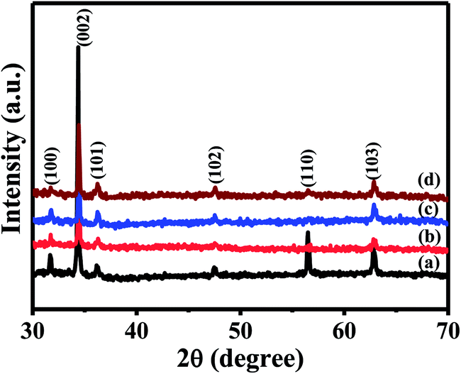 | ||
| Fig. 1 XRD patterns of as-grown (a), and 200 °C (b), 300 °C (c) and 500 °C (d) annealed ZnO NRs. | ||
Furthermore, support of the fact that the undoped and doped ZnO NRs were grown vertically on the substrate was obtained from the inset in Fig. 2(a). The FESEM images show that the NRs have a diameter in the range of 41–44 nm and a length in the range of 300–500 nm for all samples (Fig. 2). There is little change in the morphology of the NRs after the thermal treatment, except that the 300 °C and 500 °C annealed samples show a little agglomeration compared to the as-grown and 200 °C annealed samples. Our NRs are not perfectly vertical but quasi vertical (the inset in Fig. 2(a)). Therefore, the tips touching each other in few places are likely to be joined together upon annealing.
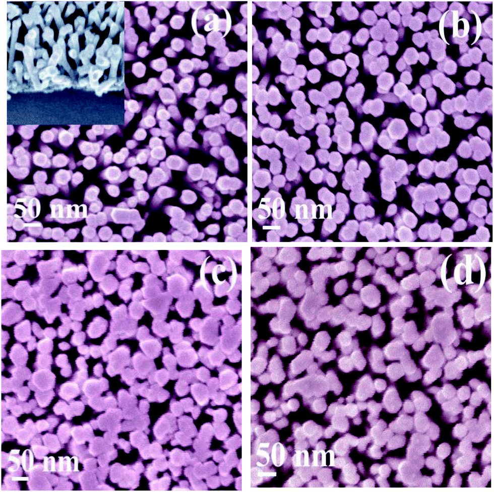 | ||
| Fig. 2 FESEM images of the as-grown (a), and 200 °C (b), 300 °C (c) and 500 °C (d) annealed ZnO NRs. The inset in (a) shows a tilted view of the quasi vertical NRs. | ||
PL and PC are two complementary processes. PL results from radiative recombinations only, while photoconductivity arises due to both radiative and nonradiative optical transitions. Fig. 3 shows the PC spectra of the as-grown and annealed ZnO NRs in the “ordinary” mode. These spectra have not been corrected for the spectral dependence of the source intensity. The spectra in general show a sharp peak below 400 nm due to band gap absorption and generation of photocarriers, and a broad hump at 450–750 nm due to photocarriers being released from different sub-band gap defect states and contributing to the corresponding PCs. The spectrum for the sample annealed at 200 °C shows a lesser current both in the visible and UV regions. With an increase in the annealing temperature, the current also increases in the visible region, especially around 430 nm to 650 nm, indicating formation of more defect states in the ZnO NRs. The ratios of Iph at 370 nm to Iph at 570 nm (Table 1) show that initially there is a tendency for a rise and then a fall in the ratio, which indicates first a betterment and then a degradation in the quality, which is at par with the PL results (discussed later). The features for the near band gap spectral region will not be discussed further, as we are only interested in sub-band gap levels.
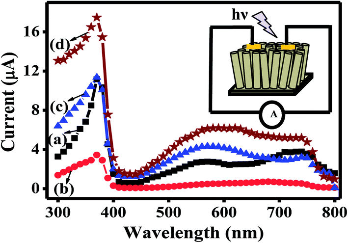 | ||
| Fig. 3 PC spectra of the as-grown (a), and 200 °C (b), 300 °C (c) and 500 °C (d) annealed ZnO NRs. The inset shows a schematic diagram of the photocurrent measurement set-up. | ||
| Annealing temperature | FWHM of UV PL peak | UV/VIS | I370 nm/I570 nm | Gr = Ired/Idc | GUV = IUV/Idc | Nred = (Gr/GUV) × 100 |
|---|---|---|---|---|---|---|
| As-grown | 19.61 | 1.14 | 4.05 | 1.54 × 10² | 2090 | 7.36 |
| 200 °C | 18.31 | 2.21 | 7.16 | 1.47 × 10³ | 16![[thin space (1/6-em)]](https://www.rsc.org/images/entities/char_2009.gif) 515 515 |
8.90 |
| 300 °C | 16.54 | 3.21 | 2.63 | 1.8 × 10³ | 14949 |
12.04 |
| 500 °C | 22.73 | 0.96 | 2.86 | 1.48 × 10³ | 5700 | 25.96 |
All the PC curves in Fig. 3 show two maximum changes in the spectrum (i.e. rises in the PC), one beyond 700 nm and one at around 570 nm. Therefore, to identify the electron traps responsible for these changes, PC transient experiments were performed by exciting the NRs first with 700 nm (red, 1.77 eV) light, then with 540 nm (green, 2.34 eV) light and finally with 360 nm (UV) light, each for 15 min, in order to vacate the traps as per their energy band positions below the conduction band (CB). Fig. 4(a) shows that the PC increases for all the samples as soon as they are exposed to 700 nm red light (1.77 eV). According to the PC spectra, it can be inferred that the carriers are released from the trap levels with energy corresponds to (Ec − 1.77 eV). To estimate this effect, for simplicity, we have assumed that the predominant effect is occurring due to one type of trap. The values of the photo-to-dark current ratios, i.e. PC gains, for red light (Ired/Idc) are 1.54 × 10² for the as-grown, and 1.47 × 10³, 1.8 × 10³ and 1.48 × 10³, respectively, for the annealed NRs (Table 1). These values suggest that maximum release of the trapped electrons occurs in the annealed samples, making the ratio higher as compared to the as-grown samples. Similarly, maximum carrier release under UV excitation after red and green excitation occurs in the as-grown sample. Given the conditions of annealing (atmosphere), excess O and/or Oi (oxygen interstitial) related defects are most likely to be formed. Presumably excess O traps occur with energy corresponds to (Ec − 1.77 eV), which causes the optical transition since the other defect, Oi, is well known to form at a level of 2.28 eV, below the CB.34,35 In agreement with this proposition, the percentage values of the released carriers (proportional to the photocurrent) due to red light excitation (Nred) shows a nonlinear increasing trend as the annealing temperature increases (Table 1).
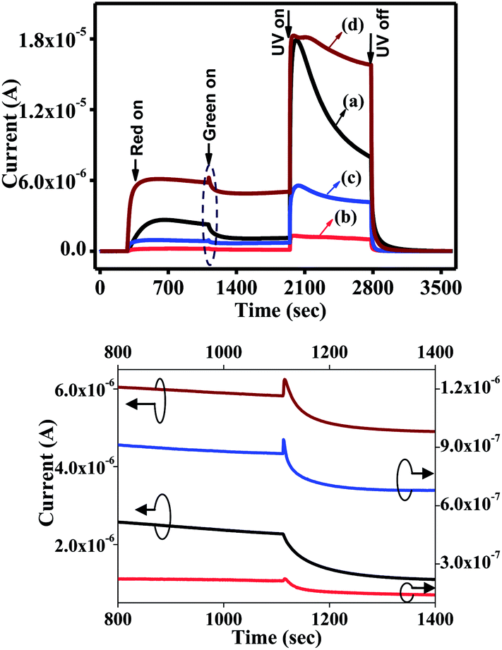 | ||
| Fig. 4 (Top) Transient PC response of the as-grown (a), and 200 °C (b), 300 °C (c) and 500 °C (d) annealed ZnO NRs. (Bottom) Magnified view of the encircled portion of the curves in the top graph. | ||
We found that interesting changes occurred for the samples under steady green light excitation. For the as-grown sample, there is no increase at all under 2.34 eV excitation, rather a fall in the photocurrent was observed (Fig. 4(b)) resulting in a negative change in the PC. This indicates the existence of a sub-band gap hole, as well as an electron trap with energy corresponds to (Ec − 2.34 eV). Trap-assisted recombination occurs when an electron falls and occupies a “trap”, and in a second step, moves into an empty valence band state, thereby completing the recombination process, referred to as Shockley–Read–Hall (SRH) recombination.36 Our transient curve in Fig. 4(a) indicates that these hole traps are much more in number in the as-grown sample, so that the recombinations in these compensates for the reduction by the excitation of holes from traps to the valence band (VB). On the contrary, for the annealed samples, Fig. 4(a) shows an initial increase and then a decrease in the photocurrent forming a ‘kink’ feature, which increases as the annealing is done at higher and higher temperatures (Fig. 4(b)). This indicates that in the annealed samples, the number of hole traps is reduced so that under excitation with 2.34 eV light, initially electrons are released from the levels lying within energy corresponds to (Ec − 1.77 eV) and (Ec − 2.34 eV), but soon hole release dominates resulting in an exponential decay in the current. Since Oi cannot be an electron trap as it is already negatively charged, the electron trap in this case most probably is VOZni i.e. (Ec − 2.16 eV).32 Next, what could be the origin of the hole traps? As the number of hole traps is decreased in the annealed samples, in all possibility, the hole traps may be VO defects (neutral or singly ionized). The explanation is as follows: Oi forms in ZnO as per equation OO = VO + Oi and a VO–Oi pair forms.37 In an annealing process, because of the oxygen ambient and Oi formation, the absorption of O atoms counteracts the formation of VO–Oi pairs and pushes the Oi atoms back to the sites of VO, reducing the number of VO, which is at par with the decrease in hole traps. According to the energy calculations and experimental results, the amount of VO in n-type ZnO is less under equilibrium conditions, as its formation energy is very high.38,39
The PL spectra of the as-grown and annealed ZnO NRs (Fig. 5) mainly consist of a UV emission peak at ∼380 nm and one or more visible bands/peaks. The intensity of the UV peak associated with free-exciton recombination across the band gap is mostly dependent on the visible emission intensity.40 The UV/VIS ratio is 1.14 for as-grown NRs, and the values are 2.21, 3.21 and 0.96, respectively, for the annealed (200 °C, 300 °C and 500 °C) NRs, which means that the UV/VIS ratio increases for the 200 °C and 300 °C annealed samples, but the ratio decreases for the 500 °C annealed sample. The FWHM of the UV peak (Table 1) slightly decreases for 200 °C and 300 °C annealing, while the value increases for 500 °C annealing. Both the changes in the intensity as well as in the FWHM values can be understood easily. The enhancement of the UV peak intensity after annealing at and above 200 °C is probably due to the desorption of hydroxyl groups at ∼150 °C.41 Therefore, by heating at a temperature of 200 °C or 300 °C, all the surface states related to OH groups or Zn(OH)2 disappear, which results in more intense UV emission as compared to the visible emission. The as-grown and 200 °C annealed samples show a broad visible band with a peak at ∼566 nm (yellow emission), which is assigned to be due to the presence of Oi.30 Shift of the peaks towards higher wavelength, i.e. orange components of the emission can be observed after annealing at a temperature of 300 °C. Red shift of the visible peak and an enhancement of its intensity occurs in the 300 °C annealed sample due to radiative recombination via VO defects, which is similar to the findings observed by Djurisic et al.24 These results are in good agreement with the PC results during green excitation, which also indicate the presence of VO-related defects. H2 desorbs at ∼420 °C.42 H2 mainly passivates the zinc vacancy (VZn) type of surface defect and helps to achieve an intense UV emission, so annealing at 500 °C releases adsorbed H2 and VZn defects become mobile within the crystal lattice worsening the FWHM value and the UV intensity.43 When annealing is performed at higher temperature, the green emission dominates, which is the predominant contribution of VZn.44–47 In other words, as per the PC results, VO cannot be the origin of the green emission. Therefore, an orange component at 610 nm appears, probably due to  .48,49
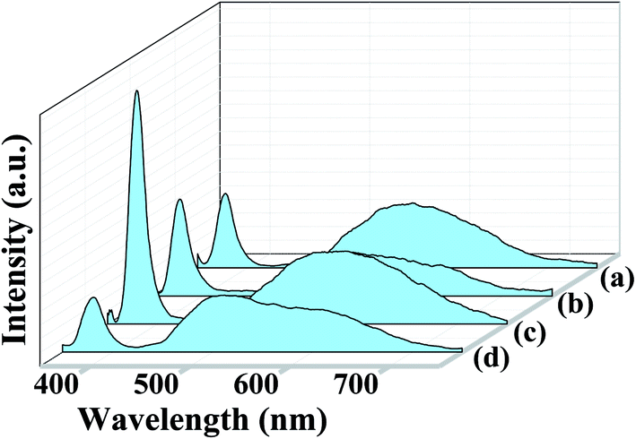 | ||
| Fig. 5 PL spectra of the as-grown (a), and 200 °C (b), 300 °C (c) and 500 °C (d) annealed ZnO NRs. | ||
Remarkably good agreement between the PL and the derivative of the PC (DPC) spectrum clearly identifies the electron and hole traps. The dI/dλ is a useful and sensitive technique to pin optical transition levels. Fig. 6(a) shows that there are three peaks in the PL spectrum at 2.03 eV (orange), 2.25 eV (yellow) and 2.42 eV (green). In the dI/dλ curve of the 500 °C annealed sample, there are ‘dip’ features at 1.93 eV, 2.06 eV, 2.29 eV, and 2.58 eV. The dips indicate either electron trap and/or hole release and/or recombinations. Matching and correlating both PL and DPC, the presence of a hole trap (VO-related) at ∼2.06 eV, and recombination centres at ∼2.25–2.29 eV (Oi) and 2.43–2.58 eV (VZn) are confirmed. The latter two therefore can be correlated to the yellow and green emissions, respectively. Based on the above results, an energy band diagram of these ZnO NRs has been proposed in Fig. 6(b).
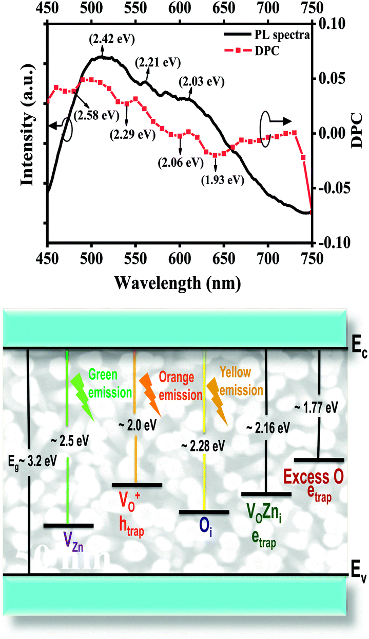 | ||
| Fig. 6 (a) PL spectra and the derivative of PC (DPC) of the ZnO NRs annealed at 500 °C. (b) Qualitative schematic of the energy band diagram of ZnO NRs. | ||
Conclusions
In summary, the sub-band gap photocurrent spectra, successive photocurrent transient spectroscopy and the derivative of the photocurrent transient spectrum of as-grown and annealed ACG ZnO NRs have been analyzed. The as-grown NR samples show fewer excess O related electron traps with energy corresponds to (Ec − 1.77 eV) and a greater number of O vacancy related hole traps, as well as fewer O interstitial related electron traps with energy corresponds to (Ec − 2.34 eV) as compared to the annealed samples. An intricate correlation between the PL and PC features in the as-grown and annealed samples has been done and accordingly a band model has been proposed showing qualitatively the electron and hole traps.Acknowledgements
The authors thank CSIR for funding the work vide project no: 03(1260)/12/EMR-II. The authors D. Sett and S. Sarkar thank CSIR, India for providing fellowships.References
- M. Afsal, C. Y. Wang, L. W. Chu, H. Ouyang and L. J. Chen, J. Mater. Chem., 2012, 22, 8420–8425 RSC.
- M. H. Huang, S. Mao, H. Feick, H. Q. Yan, Y. Y. Wu, H. Kind, E. Weber, R. Russo and P. D. Yang, Science, 2001, 292, 1897–1899 CrossRef CAS PubMed.
- J. J. Qi, X. F. Hu, Z. Z. Wang, X. Li, W. Liu and Y. Zhang, Nanoscale, 2014, 6, 6025–6029 RSC.
- S. Y. Ju, A. Facchetti, Y. Xuan, J. Liu, F. Ishikawa, P. D. Ye, C. W. Zhou, T. J. Marks and D. B. Janes, Nat. Nanotechnol., 2007, 2, 378–384 CrossRef CAS PubMed.
- Y. Qin, X. D. Wang and Z. L. Wang, Nature, 2008, 451, 809 CrossRef CAS PubMed.
- S. F. Varol, D. Sahin, M. Kompitsas and G. Cankaya, RSC Adv., 2014, 4, 13593–13600 RSC.
- H. Shen, C. X. Shan, Q. Qiao, J. S. Liu, B. H. Li and D. Z. Shen, J. Mater. Chem. C, 2013, 1, 234–237 RSC.
- Y. Z. Zheng, J. X. Zhao, H. Zhang, J. F. Chen, W. L. Zhou and X. Tao, Chem. Commun., 2011, 47, 11519–11521 RSC.
- X. L. Wu, S. J. Xiong, Z. Liu, J. Chen, J. C. Shen, T. H. Li, P. H. Wu and P. K. Chu, Nat. Nanotechnol., 2011, 6, 102–105 CrossRef PubMed.
- C. Soci, A. Zhang, B. Xiang, S. A. Dayeh, D. P. R. Aplin, J. Park, X. Y. Bao, Y. H. Lo and D. Wang, Nano Lett., 2007, 7, 1003–1009 CrossRef CAS PubMed.
- F. W. Guo, B. Yang, Y. B. Yuan, Z. G. Xiao, Q. F. Dong, Y. Bi and J. S. Huang, Nat. Nanotechnol., 2012, 7, 798–802 CrossRef CAS PubMed.
- K. Chung, C. H. Lee and G. C. Yi, Science, 2010, 330, 655–657 CrossRef CAS PubMed.
- C. Chen, H. P. He, Y. F. Lu, K. W. Wu and Z. Z. Ye, ACS Appl. Mater. Interfaces, 2013, 5, 6354–6359 CAS.
- D. Flak, A. Braun, B. S. Mun, J. B. Park, M. Parlinska-Wojtan, T. Graule and M. Rekas, Phys. Chem. Chem. Phys., 2013, 15, 1417–1430 RSC.
- C. Richter and C. A. Schmuttenmaer, Nat. Nanotechnol., 2010, 5, 769–772 CrossRef CAS PubMed.
- Y. F. Li, R. Deng, Y. F. Tian, B. Yao and T. Wu, Appl. Phys. Lett., 2012, 100, 172402 CrossRef.
- G. Rahman, N. U. Din, V. M. Garcia-Suarez and E. Kan, Phys. Rev. B: Condens. Matter Mater. Phys., 2013, 87, 205205 CrossRef.
- H. X. Chen, J. J. Ding, W. G. Guo, G. X. Chen and S. Y. Ma, RSC Adv., 2013, 3, 12327–12333 RSC.
- S. Dhara and P. K. Giri, Nanoscale Res. Lett., 2011, 6, 504 CrossRef PubMed.
- M. J. Li, G. C. Xing, G. Z. Xing, B. Wu, T. Wu, X. H. Zhang and T. C. Sum, Phys. Rev. B: Condens. Matter Mater. Phys., 2013, 87, 115309 CrossRef.
- A. Layek, B. Manna and A. Chowdhury, Chem. Phys. Lett., 2012, 539, 133–138 CrossRef.
- J. Kossmann and C. Hattig, Phys. Chem. Chem. Phys., 2012, 14, 16392–16399 RSC.
- P. S. Venkatesh, V. Purushothaman, S. E. Muthu, S. Arumugam, V. Ramakrishnan, K. Jeganathan and K. Ramamurthi, CrystEngComm, 2012, 14, 4713–4718 RSC.
- A. B. Djurisic, Y. H. Leung, K. H. Tam, Y. F. Hsu, L. Ding, W. K. Ge, Y. C. Zhong, K. S. Wong, W. K. Chan, H. L. Tam, K. W. Cheah, W. M. Kwok and D. L. Phillips, Nanotechnology, 2007, 18, 095702 CrossRef.
- S. Dhara and P. K. Giri, J. Appl. Phys., 2011, 110, 124317 CrossRef.
- S. K. Mishra, R. K. Srivastava, S. G. Prakash, R. S. Yadav and A. C. Panday, Opto-Electron. Rev., 2010, 18, 467–473 CAS.
- S. Dhara and P. K. Giri, J. Appl. Phys., 2012, 111, 044320 CrossRef.
- S. Panigrahi and D. Basak, Nanoscale, 2011, 3, 2336–2341 RSC.
- A. Bera, T. Ghosh and D. Basak, ACS Appl. Mater. Interfaces, 2010, 2, 2898–2903 CAS.
- P. P. Das, S. A. Agarkar, S. Mukhopadhyay, U. Manju, S. B. Ogale and P. S. Devi, Inorg. Chem., 2014, 53, 3961–3972 CrossRef CAS PubMed.
- X. Y. Xu, C. X. Xu, Y. Lin, J. T. Li and J. G. Hu, J. Phys. Chem. C, 2013, 117, 24549–24553 CAS.
- K. H. Tam, C. K. Cheung, Y. H. Leung, A. B. Djurisic, C. C. Ling, C. D. Beling, S. Fung, W. M. Kwok, W. K. Chan, D. L. Phillips, L. Ding and W. K. Ge, J. Phys. Chem. B, 2006, 110, 20865–20871 CrossRef CAS PubMed.
- J. J. Zhang, E. J. Guo, L. P. Wang, H. Y. Yue, G. J. Cao and L. Song, Trans. Nonferrous Met. Soc. China, 2014, 24, 736–742 CrossRef CAS.
- S. Kuriakose, B. Satpati and S. Mohapatra, Phys. Chem. Chem. Phys., 2014, 16, 12741–12749 RSC.
- A. B. Djurisic and Y. H. Leung, Small, 2006, 2, 944–961 CrossRef CAS PubMed.
- A. Schenk, Solid-State Electron., 1992, 35, 1585–1596 CrossRef CAS.
- H. B. Fan, S. Y. Yang, P. F. Zhang, H. Y. Wei, X. L. Liu, C. M. Jiao, Q. S. Zhu, Y. H. Chen and Z. G. Wang, Chin. Phys. Lett., 2007, 24, 2108–2111 CrossRef CAS.
- A. Janotti and C. G. Van de Walle, Phys. Rev. B: Condens. Matter Mater. Phys., 2007, 76, 165202 CrossRef.
- F. Tuomisto, K. Saarinen, D. C. Look and G. C. Farlow, Phys. Rev. B: Condens. Matter Mater. Phys., 2005, 72, 085206 CrossRef.
- A. van Dijken, E. A. Meulenkamp, D. Vanmaekelbergh and A. Meijerink, J. Lumin., 2000, 87–89, 454–456 CrossRef CAS.
- Y. F. Yao, C. H. Shen, W. F. Chen, P. Y. Shih, W. H. Chou, C. Y. Su, H. S. Chen, C. H. Liao, W. M. Chang, Y. W. Kiang and C. C. Yang, J. Nanomater., 2014, 756401 Search PubMed.
- R. G. Xie, T. Sekiguchi, T. Ishigaki, N. Ohashi, D. S. Li, D. R. Yang, B. D. Liu and Y. S. Bando, Appl. Phys. Lett., 2006, 88, 134103 CrossRef.
- A. Bera and D. Basak, Appl. Phys. Lett., 2009, 94, 163119 CrossRef.
- A. Janotti and C. G. Van de Walle, Rep. Prog. Phys., 2009, 72, 126501 CrossRef.
- F. Fabbri, M. Villani, A. Catellani, A. Calzolari, G. Cicero, D. Calestani, G. Calestani, A. Zappettini, B. Dierre, T. Sekiguchi and G. Salviati, Sci. Rep., 2014, 4, 5158 CAS.
- Y. H. Leung, X. Y. Chen, A. M. C. Ng, M. Y. Guo, F. Z. Liu, A. B. Djurisic, W. K. Chan, X. Q. Shi and M. A. Van Hove, Appl. Surf. Sci., 2013, 271, 202–209 CrossRef CAS.
- J. P. Lv, C. D. Li and J. J. BelBruno, CrystEngComm, 2013, 15, 5620–5625 RSC.
- A. B. Djurisic, Y. H. Leung, K. H. Tam, L. Ding, W. K. Ge, H. Y. Chen and S. Gwo, Appl. Phys. Lett., 2006, 88, 103107 CrossRef.
- Q. Zhu, C. S. Xie, H. Y. Li, C. Q. Yang, S. P. Zhang and D. W. Zeng, J. Mater. Chem. C, 2014, 2, 4566–4580 RSC.
| This journal is © The Royal Society of Chemistry 2014 |