Qifan Xue‡
,
Zhicheng Hu‡,
Chen Sun,
Ziming Chen,
Fei Huang*,
Hin-Lap Yip* and
Yong Cao
Institute of Polymer Optoelectronic Materials and Devices, State Key Laboratory of Luminescent Materials and Devices, South China University of Technology, Guangzhou 510640, P. R. China. E-mail: msangusyip@scut.edu.cn; msfhuang@scut.edu.cn
First published on 25th November 2014
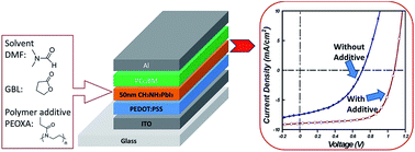
A polymer with tailored chemical functionality was introduced as a processing additive to control the film formation of the CH3NH3PbI3 perovskite structure, leading to enhanced photovoltaic performance in a PEDOT:PSS/perovskite/PCBM-based planar heterojunction solar cell under optimized conditions. By adjusting the polymer doping content and the processing solvent, the grain size, film coverage and the optical properties of the perovskite films can be effectively tuned. At optimized conditions, the planar heterojunction solar cell composed of a thin layer of perovskite–polymer film (∼50 nm) exhibits an average PCE of 6.16% with a Voc of 1.04 V, a Jsc of 8.85 mA cm−2 and a FF of 0.65, which are much higher than those of the control device with a pristine perovskite film. The higher performance was attributed to improved morphology and interfaces of the perovskite–polymer films, which reduced the undesired contact between PEDOT:PSS and PCBM and minimized the shunting paths in the device. In addition, since the fabrication process for the perovskite solar cells can be performed at low temperature, flexible cells built on plastic substrates can therefore be realized with a PCE of 4.35%.
The perovskite semiconductors can also be adopted in various types of solar cell architectures including perovskite-sensitized solar cells, meso-superstructured solar cells and planar p–i–n heterojunction solar cells.1–9 The latter is particularly attractive for potential commercialization due to the simplicity of the device structure, the low-temperature solution processability and the potential of large-scale manufacturing of the perovskite cells using a continuous coating technique on flexible substrates.8,16–18
There are several issues that need to be addressed in order to improve the performance of planar heterojunction perovskite cells. First, interfacial materials with good charge selectivity are required to reduce interfacial charge recombination. In a typical p–i–n planar heterojunction structure, the perovskite thin film is sandwiched between a hole selective layer (e.g. PEDOT:PSS) and an electron selective layer (e.g. PCBM) while a transparent ITO-coated glass substrate and a low work function metal are used as anode and cathode, respectively. (Fig. 1a) This structure is advantageous as both the interlayers can be processed at low temperatures and also have proven processability using large-area coating technique as demonstrated in roll-to-roll manufactured organic photovoltaic devices.20–23
![]() | ||
Fig. 1 (a) Device structure of the hybrid planar heterojunction solar cell and the molecular structure of the solvents and polymer additive used in this study. (b) Schematic drawing of the energy levels and thickness of each layer in the device. The energy levels are taken from literature.15,16,25 |
Second, the quality of the perovskite films including the crystallinity, morphology and coverage also need to be optimized in order to improve the performance of the perovskite solar cells.20,24–28 Snaith et al. showed that the crystallization rate of perovskite films could be controlled using mixed halide such as CH3NH3PbI3−xClx.29,30 Prolonging the crystallization and growth process in mixed halide perovskites provides better processing window to prepare good quality films with high coverage, which is crucial to improve the performance of the solar cells. Adding high boiling point solvent additive to the mixed halide perovskite solution also proved to be an efficient way to modulate the perovskite film morphology.26 However, the relatively long annealing time and the difficulty in controlling the final stoichiometry are the drawbacks for the mixed halide perovskites.14,15,26
CH3NH3PbI3 is structurally more simple but it remains a challenge to control the crystallization process and the quality of the perovskite films.17,18,31 Although several methods including the use of mixed solvents,32 control of precursor concentration and film drying rate,17,31 and a novel two-step deposition process has been developed to improve the morphology and coverage of the CH3NH3PbI3 films,7,8,33,34 there is still considerable room to further improve the perovskite solar cell performance by introducing a new processing strategy to effectively manipulate the perovskite film morphology.
In this work, a polymer additive with tailored chemical functionality was introduced into the CH3NH3PbI3 perovskite structure to control the crystallization process and morphology of the perovskite films. The process–structure–performance relationships of the perovskite solar cells were studied. We found that the performance of the planar heterojunction perovskite solar cells with device structure of ITO/PEDOT:PSS/CH3NH3PbI3 Polymer/PC61BM/Al (Fig. 1a and b) was strongly dependent on the choice of solvents and also the content of polymer additive in the perovskite precursor solutions. At optimized conditions, the best performing planar heterojunction solar cells composed of a thin layer of CH3NH3PbI3 perovskite–polymer composite film (∼50 nm) exhibits a PCE of 6.35% with a Voc of 1.07 V, a Jsc of 8.95 mA cm−2 and a FF of 0.66, which are much higher than those of the control device with a pristine perovskite film. In addition, by taking the advantage of low temperature processes required for the fabrication of the perovskite solar cells, we successfully demonstrated flexible cells on ITO-coated poly(ethylene terephthalate) (PET) substrates.
Current density–voltage (J–V) characteristics for the devices were measured under 100 mW cm−2 air mass 1.5 global (AM 1.5 G) illumination with a solar simulator (Oriel model 91192). The light intensity was calibrated using an National Renewable Energy Laboratory (NREL) calibrated silicon photodiode with a KG5 filter. UV-vis absorption and photoluminescence spectra were recorded on a HP 8453 spectrophotometer and FLS920 spectrofluorimeter (Edinburgh), respectively. The SEM images were obtained using a Zeiss EVO 18 scanning electron microscopy. Atom force microscopy (AFM) measurements were carried out using a Digital Instrumental DI Multimode Nanoscope IIIa in tapping mode. The crystal structure of CH3NH3PbI3–PEOXA films was investigated with an X-ray diffractometer (PANalytical X'pert PRO) equipped with a Cu-Kα X-ray tube. With a scan angle of 1° and a step size of 0.04° as well as a time step of 3 s, we carried out the acquisition in the range of 10–60° in θ–2θ mode.
With increasing content of PEOXA in the perovskite films, the XRD peak intensity of CH3NH3PbI3 films decreased and the peaks were nearly completely diminished after adding 3 wt% of PEOXA. However, the peak positions did not change with the PEOXA content, indicating that the crystal structure remained but only the crystallinity of the film decreased. SEM images revealed that the perovskite films deposited on PEDOT:PSS coated ITO appeared as a form of needle-like crystals randomly distributed on the surface (Fig. 2b). The crystals only partially covered the substrate leaving part of the PEDOT:PSS exposed. Upon adding the PEOXA, the film morphology became more uniform and the coverage increased. The needle-like crystals were also found to break down with increasing PEOXA doping and it became a featureless, smooth film when 3 wt% of PEOXA was added. The change of morphology upon PEOXA addition is in agreement with the XRD data as the crystallinity is decreased with increasing PEOXA content.
Based on the trend observed by XRD and SEM, we conclude that PEOXA can interact strongly with the CH3NH3PbI3 and significantly suppress the growth of the perovskite crystal.
To study the polymer additive effect on the performance of the perovskite solar cells, we fabricated perovskite/fullerene planar heterojunction solar cells based on the structure of ITO/PEDOT:PSS/Perovskite/PCBM/Al and the J–V curves and the performance parameters are shown in Fig. 2c and Table 1, respectively. The solar cells based on the pristine CH3NH3PbI3 film processed from DMF delivered an average PCE of 4.21% with Voc, Jsc and FF equal to 0.82 V, 7.78 mA cm−2 and 0.634, respectively. These results are comparable to that in other reports with similar device structure.18 The device performance deteriorated with increasing content of PEOXA and the PCE dropped to ∼1.5% with lost in all PV parameters. We attribute that to the breakdown of the CH3NH3PbI3 perovskite structure. When the content of PEOXA increased to 3 wt%, no obvious photovoltaic effect could be observed in our solar cells due to the amorphous nature of the perovskite film.
Voc (V) | Jsc (mA cm−2) | FF(%) | PCE(%) | |
---|---|---|---|---|
0 wt% PEOXA | 0.82 ± 0.03 | 7.78 ± 0.24 | 63.4 ± 1.2 | 4.21 ± 0.21 |
0.75 wt% PEOXA | 0.64 ± 0.01 | 4.46 ± 0.11 | 49.1 ± 1.9 | 1.43 ± 0.08 |
1.5 wt% PEOXA | 0.50 ± 0.01 | 4.02 ± 0.19 | 58.7 ± 2.3 | 1.14 ± 0.19 |
Thicker perovskite films are typical required to achieve high Jsc. However, it is challenging to obtain smooth and thick CH3NH3PbI3 films through one-step solution process as the crystal growth process of perovskite is difficult to control. A commonly used approach to overcome this problem is to use mixed halide perovskite such as CH3NH3PbIxCl3−x, which allows to form relative thick and smooth film with enhanced light harvesting property. To study the effect of PEOXA doping on the thicker perovskite films, we introduced smaller amount of PEOXA into the CH3NH3PbIxCl3−x precursor solution with DMF as the solvent. The control device based on the 300 nm pristine mixed halide perovskite film showed an average PCE of 9.47% with Voc, Jsc and FF equal to 0.90 V, 18.21 mA cm−2 and 0.572, respectively. The devices with 0.25 wt% PEOXA doping delivered a lower average PCE of 8.96% with Voc, Jsc and FF equal to 0.87 V, 17.93 mA cm−2 and 0.568 while the one doped with 0.75 wt% PEOXA showed even lower performance. (See ESI: Table S1, Fig. S2 and S3†). These results are in good agreement with the CH3NH3PbI3-based devices. Encouragingly, the standard derivation of the PEOXA doping device performance was lower compared to the reference device.
Considering that the strong interactions among DMF, PEOXA and the perovskite will significantly suppress the crystal growth of the perovskite film, we therefore chose GBL as another processing solvent for our study aiming to reduce the interactions among the solvent, polymer and perovskite and provide better control over the microstructure of the films. In addition, from the environmental aspect, GBL is a less hazardous solvent compared to DMF as it can be biodegradable while DMF is much more toxic.
The SEM images of the perovskite films spun cast on ITO/PEDOT:PSS substrates are shown in Fig. 3b. Different from the needle-like crystals observed in the DMF-processed films, the pristine CH3NH3PbI3 film processed from GBL exhibited disk-like crystal structure with irregular shapes and very rough edges. The crystals were disconnected leaving a large portion of uncovered area with exposed PEDOT:PSS film. The average size of the crystal was about 2 μm. Upon adding the PEOXA additive, the crystal domains became more homogenous and the size of the crystals and also the average uncovered area decreased with increasing content of the PEOXA.
The greater coverage of the CH3NH3PbI3–PEOXA film may reduce the chance of direct contact between PC61BM and PEDOT:PSS layer and minimize the shunting paths in the solar cells. To further evaluate the topography and the height profile of the perovskite–PEOXA films, atomic force microscopy (AFM) study were performed. (Fig. 3c and S1†). The surface of the pristine CH3NH3PbI3 film was relatively rough, with the root-mean-square (RMS) roughness of 27.3 nm. Upon adding the polymer additive, the surface of the CH3NH3PbI3–PEOXA composite films became smoother, with the RMS of 21.5, 20.4, 18.0, 16.7 and 9.9 nm for the films with 1 wt%, 1.5 wt%, 3 wt%, 5 wt% and 7 wt% of PEOXA, respectively. (Fig. S1†) The observed evolution of the morphology of the perovskite films from the AFM study is in good agreement with that observed by SEM. To further study how the PC61BM film form on the perovskite films, we also studied the morphology of the PC61BM film coated on the CH3NH3PbI3–PEOXA (1.5 wt%) film as an example and the corresponding AFM image is shown in Fig. 3c. Instead of forming a flat film, the 25 nm PC61BM homogeneously coated on the composite film with surface topology replicated that of the underneath film but with a smaller RMS roughness of 6.9 nm. The good coverage of PC61BM is important as it allows homojunction formation between the PC61BM buffer layer and the Al cathode and reduces the undesired contact between the perovskite film and the metal cathode.
The optical properties of the perovskite and composite films were studied and their absorption and photoluminescence (PL) spectra are shown in Fig. 4a and b, respectively. A typical absorption spectrum for the pristine CH3NH3PbI3 film was obtained with absorption edge at 780 nm, which corresponds to a bandgap of 1.50 eV and is consistent with previous reports.8,18,31 The absorbance of the perovskite films decreased with increasing content of the PEOXA, while the shape of the absorption curves remained the same. We attribute the decrease in absorbance to the reduced crystallinity of the perovskite in the composite films as observed from the XRD study. The steady-state PL study revealed a very interesting emission property of the studied films. The emission peak of the pristine CH3NH3PbI3 film at ∼780 nm was corresponding to the nanocrystalline perovskite particles as suggested by Choi et al. and other reports.19,32,37,38 Highly crystalline bulk CH3NH3PbI3 is a poor emitter with emission peak over 800 nm that we did not observe in our study.37 Upon introduction of the PEOXA, a blue-shifted PL peak arose at 710 nm and this peak was increased with PEOXA content while the PL peak at 780 nm decreased accordingly. The feature peak at 710 nm has not been reported before and we attribute that to the emission from a more disordered perovskite phase resulted from the strong interaction with the PEOXA. The PL peak intensity at 710 nm increased with the PEOXA content is also in agreement with the fact that the emission property of the perovskite can enhance when the crystallinity decreased.37–40 It is worth noting that despite a distinct emission property was found in the composite films, the similarity in the absorption edge of those films indicated that there is an insignificant change in bandgap.
The performances of the perovskite planar heterojunction solar cells processed from GBL are summarized in Table 2 and Fig. 5. Solar cells based on the pristine CH3NH3PbI3 perovskite film delivered a lower performance compared to that processed from DMF, with a Voc of 0.71 V, a Jsc of 7.47 mA cm−2, a FF of 0.45 and a corresponding PCE of 2.37%. We attribute the lower performance to the reduced coverage of the perovskite film and the presence of large amount of PbI2 phase. However, when a small amount of PEOXA was introduced in the perovskite films, the performance of the solar cells significantly improved with all three photovoltaic parameters improving simultaneously at optimized conditions. In general, the Voc of the devices with PEOXA doping is much higher than that from the pristine perovskite film. It increased with the PEOXA content reaching a maximum Voc of 1.1 V at 3 and 5 wt% doping concentration before decreasing again at higher doping concentration. It is worth to note that typically the Voc for the best solution-processed CH3NH3PbI3/PCBM planar heterojunction solar cells are only in the range of 0.8–0.9 V.17,18,31 A Voc of 1.1 V was only achieved in the high performance Al2O3-based meso-superstructured perovskite solar cells and vapor-deposited perovskite solar cells.4–6,9,41 We attribute the improved Voc not only to the higher coverage of the perovskite–polymer film, but also to the reduced number of contacts between PEDOT:PSS/PCBM as a thin layer of PEOXA may block the undesired PEDOT:PSS/PCBM contact which can act as a charge recombination site.11 A little drop of the Voc at the 7 wt% PEOXA-doped device may be due to the formation of a relatively thick insulating PEOXA layer at the device junction, forming a poor diode as revealed by the low FF of the device. Therefore, the strategy demonstrated here is an important means to further enhance the performance of perovskite/fullerene-based solar cells.
Voc (V) | Jsc (mA cm−2) | FF (%) | PCE (%) | Rs (Ω cm2) | Rp (Ω cm2) | |
---|---|---|---|---|---|---|
0 wt% PEOXA | 0.68 ± 0.02 | 7.27 ± 0.13 | 42.4 ± 2.1 | 2.13 ± 0.28 | 25 ± 4 | 380 ± 30 |
1 wt% PEOXA | 0.90 ± 0.03 | 7.54 ± 0.38 | 66.5 ± 1.7 | 4.65 ± 0.31 | 13 ± 2 | 1024 ± 32 |
1.5 wt% PEOXA | 1.04 ± 0.03 | 8.85 ± 0.15 | 65.2 ± 1.3 | 6.16 ± 0.18 | 7 ± 2 | 1328 ± 101 |
3 wt% PEOXA | 1.08 ± 0.01 | 6.69 ± 0.12 | 60.3 ± 2.5 | 4.49 ± 0.15 | 16 ± 3 | 968 ± 120 |
5 wt% PEOXA | 1.09 ± 0.01 | 6.87 ± 0.22 | 50.5 ± 4.6 | 4.12 ± 0.12 | 22 ± 2 | 1205 ± 301 |
7 wt% PEOXA | 0.98 ± 0.03 | 2.44 ± 0.15 | 40.4 ± 2.3 | 0.91 ± 0.13 | 108 ± 28 | 1009 ± 185 |
In addition to the improvement of Voc, an increase in Jsc and FF were also found when an appropriate amount of PEOXA was added to the perovskite films. The Jsc increased from 7.47 mA cm−2 in the pristine film to 8.95 mA cm−2 at 1.5 wt% PEOXA doping and then plateaued at ∼7 mA cm−2 at higher wt% PEOXA doping before significantly dropping to ∼2.5 mA cm−2 at 7 wt% doping. The increase in Jsc cannot be simply explained by the absorption spectra of the films as the pristine film showed the largest absorbance. Therefore the improved charge generation and extraction at optimized perovskite/PEOXA film may account for the increase in Jsc. To study the spectral response of the different devices. The incident photon to electron conversion efficiency (IPCE) measurement was performed and the result are shown in Fig. 5. The 1.5 wt% PEOXA doped devices showed a marked enhancement of the IPCE with a broad spectral response in the region from the visible to near-infrared and reached a peak of 48% at ∼450 nm.
Considering a relatively thin perovskite film with nominal thickness of ∼50 nm was used, the Jsc and IPCE values are quite high indicating the perovskite is an excellent light absorber. The FF is another parameter that improved with the addition of PEOXA. The FF is governed by both the parasitic series resistance (Rs) and shunt resistance (Rp) of the solar cells.42–44 Typically Rs is determined by the bulk conductivity of the electrodes, active and interfacial layers, and the contact resistance between them while Rp is determined by the quality of the films and their interfaces. In our study the Rs and Rp were extracted by fitting the J–V curves with Lambert W function to help to analyze the FF of different devices and the corresponding data are summarized in Table 2.42,43,45,46 When small amount of PEOXA was added, a high FF over 60% was achieved with both the Rs and Rp improved over the devices with pristine film. Taking the 1.5 wt% PEOXA doped devices as an example, a low Rs of 10 Ω cm2 and a high Rp of 1468 Ω cm2 were achieved while the pristine film showed a relatively high Rs of 29 Ω cm2 and a lower Rp of 410 Ω cm2. We suggest that despite a higher crystallinity found in the pristine film, the very rough edges of the irregular perovskite crystal domains as observed by the SEM study might act as charge scattering centers which affected the charge transport property of the film. While the well-defined crystal domains with smoother edges in the composite films could possess better charge transport properties and therefore accounts for the reduction of Rs. However, at very high PEOXA doping concentration the Rs of the corresponding devices were increased again due to the insulating property of the polymer additive.
Regarding to the Rp, we attribute the improvement of the composite films to the improved selective contact at the anode since a thin layer of PEOXA coated on the PEDOT:PSS could prevent it from directly contact with the PCBM through the uncovered void area of the perovskite film. It was previously reported that such a PEDOT:PSS/PCBM contact can form shunting paths not only affects the diode characteristic but also limits the Voc of the perovskite solar cells.29 The significant increase in the Rp suggested that the charge leaking at the anode interface was efficiently suppressed. The improved diode behavior of the PEOXA-doped devices can also be seen in the reduced dark current at the reversed bias region in the J–V plot as shown in Fig. 5c, resulting in devices with better rectification and FF. With the simultaneous improvement in all the three device-related parameters, the best solar cell performance was achieved at the optimized 1.5 wt% PEOXA doping showing a PCE up to 6.35% with a Voc of 1.07 V, a Jsc of 8.95 mA cm−2 and a FF of 0.66. It is also worth noting that the standard derivation of the device performance is lower when compared to other reported perovskite solar cells,5,8,16 indicating that the device reproducibility can be improved by employing a perovskite–polymer composite film.
Finally, taking advantage of the low temperature processes (<150 °C) required for the fabrication of the perov-skite/fullerene planar heterojunction cells,16,47 we further demonstrated the possibility for making flexible devices on plastic substrates. Flexible hybrid planar heterojunction solar cells were fabricated on ITO-coated poly(ethylene terephthalate) (PET) substrates based on the optimal conditions (CH3NH3PbI3-1.5 wt% PEOXA), giving a PCE of 4.35% with an Voc of 1.05 V, a Jsc of 7.38 mA cm−2, a FF of 0.573 (Fig. 6). Relative to the device performance based on the ITO-coated glass (PCE: 6.35%, Voc: 1.07 V, Jsc: 8.95 mA cm−2, FF: 0.662), Voc remain constant and the lower efficiency may be due to intrinsic limitations of PET plastic substrate including the lower optical transmittance (Fig. S7†) and higher ITO sheet resistance (60 Ω sq−1 vs. 15 Ω sq−1).
Footnotes |
† Electronic supplementary information (ESI) available. See DOI: 10.1039/c4ra11739e |
‡ These authors contributed equally to this work. |
This journal is © The Royal Society of Chemistry 2015 |