Butterfly-scale architecture directed electrodeposition of Ag microband arrays for electrochemical detection

Xingmei Guo, Tang Zhang, Jingwen Li and Tongxiang Fan*
State Key Lab of Metal Matrix Composites, Shanghai Jiaotong University, Shanghai, 200240, P. R. China. E-mail: txfan@sjtu.edu.cn

Received 25th September 2014 , Accepted 4th November 2014

First published on 4th November 2014


Abstract

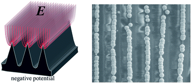
Butterfly scales with various elaborate architectures provide a large pool for structural design of microelectrode array arrangements. Here, the ridge array architecture of Troides aeacus butterfly scales was used as guidance to gather an electric field compactly around the ridge tips when a cathode potential was exerted. This tip effect directed the electrodeposition of Ag into microband arrays, on which effective electrochemical detection of hydrogen peroxide was achieved.


Microelectrode arrays attract a lot of attention due to their fundamental significance and potential applications in the electrochemical arena, such as in electroanalysis and biosensing.1–4 Great advantages including enhanced mass transport, lowered detection limit, improved signal-to-noise ratio, etc. have been demonstrated on microelectrode arrays.1,5,6 However, developing a low-cost and high-throughput technique for widespread fabrication remains a challenge.1,7 For example, modern techniques are often involved for fabricating architectures in micro/nano scale, such as lithography and nanoimprinting, which are usually costly, low-throughput and time-consuming; while the frequently used template assisted methods, such as anodised aluminium oxide templating, can only achieve micro- or nano-ensembles with unsatisfying regularity and limited patterns.1,2,5–12 It is urgently required to develop an efficient and inexpensive way to obtain highly ordered microelectrode arrays with good variety and precise control. Butterfly, nearly 20[thin space (1/6-em)]000 types of which are identified solely by the patterns of their wings, comprises scales with different complex microarchitectures.13,14 This provides a great template warehouse for structural design of microelectrode arrangement.

Microband arrays as a type of microelectrode arrays are designed with one microscopic critical dimension to impart microelectrode behavior, such as enhanced sensitivity, while the other dimension is made larger to assure high signal current.15 The interaction or overlapping of diffusion fields for electrolyte to each individual microband directly determines the electrochemical output of the macro electrode.16 Here, we used a simple electrodeposition method to synthesize Ag microband arrays. Carbonized Troides aeacus butterfly-scales with inverse-V type ridge array architecture were prepared as electrode substrates on which solid Ag was deposited from electrolyte under negative potentials. The formation of microband arrays with precise periodic distance was essentially directed by the uneven electric field intensity (E) around the ridge tips due to high structural curvature, or in other words, the tip effect, which caused accumulated electromigration and easier deposition behavior along the ridges (Scheme 1). Recent effort on synthesizing metal microarrays by electrodeposition is rare and mainly focused on using highly oriented pyrolytic graphite (HOPG) as substrates to deposit Ag, Pd, etc. onto the edge-plane step defects that exhibit relatively high electrochemical activity.17–19 However, the edge-plane steps are not regularly arranged to form highly periodic arrays, and what's more, it is often difficult to entirely exclude the interference of basal-planes as well.20 This work, in contrast, tackled the above mentioned problems. Additionally, the ridge array architecture used here is only one of the elaborate architectures in thousands butterfly species.13 The great variety of butterfly-scale architectures makes possible the design and fabrication of other micro-/nano-arrangements using the electric field driven deposition method.


image file: c4ra11189c-s1.tif
Scheme 1 Schematic diagram showing the process of butterfly-scale architecture directed electrodeposition of Ag microband arrays. The below box: the schematic drawing of the tip effect for electric field intensity (E).

The original composition of butterfly-scales is chitin,21 a carbohydrate which can be easily converted into carbon by vacuum pyrolysis method. As shown in Fig. S1, the architecture of Troides aeacus butterfly-scales is characterized by evenly spaced inverse-V type ridge arrays. The ridge height is about 5.0 μm and the periodic distance between two ridges is about 2.3 μm. After carbonization, as shown in Fig. S2, the ridge array architecture retained perfectly with certain shrinkages compared to original dimension. The ridge height was about 4.0 μm with a periodic distance of about 2.0 μm for the carbonized architecture. XRD patterns in Fig. S3 demonstrates the amorphous carbon character of carbonized butterfly-scales. Raman spectra verified the existence of abundant sp2 bonding in the amorphous sample.22,23 The carbonized wing samples were then fixed onto indium–tin-oxide (ITO) glass slides and used as substrates for electrodeposition using chronoamperometry method. A negative potential was exerted on the ridge array architectured carbon which was immersed in the electrolyte containing [Ag(NH3)2]+ for a certain period to achieve Ag deposition microband arrays. All potentials reported in this work were referred to saturated calomel electrode (SCE). Detailed processes for electrode fabrication and electrodeposition are shown in ESI S1 and S2.

The electrodeposition of Ag comprises two crucial processes: nuclei formation and nuclei growth. The number and size of Ag nuclei here are controlled by the exerted potential, which is expressed by the electrochemical version of Kelvin equation.24

 
image file: c4ra11189c-t1.tif(1)
where r means the critical nucleation radius, |η| the overpotential, σ the specific surface energy, V the atomic volume in the crystal, z the number of elementary charges e0. Eqn (1) reveals that the formation of smaller nuclei needs more negative potential (higher overpotential) which comes with higher current density leading to higher nuclei formation rate.25

Fig. 1 shows the Ag deposition morphology achieved under different potentials for 60 s and 90 s, respectively. It is obvious that the optimum electrodepositing potential to obtain Ag microband arrays was −0.9 V, when large amounts of nuclei formed on the ridge tips in the early stage; then the small particles grew regularly to contact with each other and to form microband Ag along the inverse-V type ridges (Fig. 1e and f). The periodic distance of the microband arrays was 2.0 μm coincide with the ridge array architecture period, and the Ag particle size was about 560 nm after electrodeposition for 90 s. However, irregular growth would occur for longer deposition time (Fig. S4). For less negative potentials at −0.5 V and −0.7 V, Ag particles were too dispersed to form microband arrays, because the overpotential was not big enough to form plenty nuclei in the nucleation stage (Fig. 1a–d). In contrast, however, for more negative potential at −1.0 V, the driving force was too big that dendritic structure formed on the ridge arrays (Fig. 1g and h), which would lead to more random and irregular dendrite morphology at extensive deposition time (Fig. S5). Or in other words, the deposition process became diffusion-controlled at high overpotentials and the sharp concentration drop of [Ag(NH3)2]+ in the electrode vicinity lead to concentration polarization and irregular nuclei growth.25


image file: c4ra11189c-f1.tif
Fig. 1 FESEM images showing the Ag deposition morphology achieved under different conditions. (a and b) −0.5 V for 60 s and 90 s, respectively. (c and d) −0.7 V for 60 s and 90 s, respectively. (e and f) −0.9 V for 60 s and 90 s, respectively. (g and h) −1.0 V for 60 s and 90 s, respectively. Scale bar: 2 μm for all.

The amount of Ag deposited on electrode can be calculated from the charge quantity during the electrodeposition process based on the chronoamperometric curve (Fig. S6). The Ag loading was estimated to be 0.22 mg cm−2 on the electrode surface. Also, Ag microband arrays only occupied 28% of the apparent electrode area which can be easily estimated from the FESEM image (Fig. 1f) considering the high periodicity and regularity. Ag composition was demonstrated by energy dispersive spectra (EDS) (Fig. S7 and S8). To further determine the status of deposited silver, X-ray photoelectron spectrum (XPS) was achieved, as shown in Fig. 2. The peaks of binding energies at 367.9 and 373.9 eV can be assigned to Ag 3d5/2 and Ag 3d3/2, respectively, which are in agreement with metallic silver.26


image file: c4ra11189c-f2.tif
Fig. 2 XPS for Ag deposition.

In order to demonstrate the tip effect for E around the ridge array architecture and verify the electrodeposition behavior along ridge arrays, finite element simulations were further conducted using Comsol Multiphysics 4.2 software. The domain approach was used with a one-ridge period as a domain unit in the modeling and simulating process.27 (See ESI S3 for detailed information) According to Fig. 3a, E was distributed evenly in the bulk solution; however, remarkable high E occurred around the ridge tips of the electrode and the tip effect for E was more obvious at higher overpotentials. Simulated morphology for metal electrodeposition achieved by chronoamperometry for different duration time is displayed in Fig. 3b, which directly demonstrates the preferable metallic nucleation and growth on ridge tips.


image file: c4ra11189c-f3.tif
Fig. 3 (a) Simulated electric field intensity (E) distribution at inverse-V type ridge array architecture and local bulk solution under overpotential of −0.5 V (1), −0.7 V (2), and −0.9 V (3), respectively. (b) Electrolyte concentration profile, isopotential lines, current density streamlines, and deposition morphology under −0.9 V for 30 s (1), 60 s (2), and 90 s (3), respectively.

In order to investigate the electrochemical detection performance on the Ag microband arrays, hydrogen peroxide was chosen as representative object here. According to the cyclic voltammograms shown in Fig. 4a, the Ag deposition had evident electrocatalytic activity for reduction of H2O2. As the potential swept to the negative direction, the reduction current increased obviously until forming a broad bump around −0.35 V. The amperometric result on the Ag microband array electrode with successive addition of different quantity of H2O2 in 0.1 M phosphate buffer solution (PBS) at an applied potential of −0.4 V was shown in Fig. 4b. The response time was less than 3 s to reach 95% of the steady-state current. A wide linear response in the range from 20 μM to 23 mM (R2 = 0.996) and high sensitivity of 27.1 μA (mM−1 cm−2) or 123.2 μA (mM−1 mgAg−1) was achieved. The detection limit estimated as three times of standard derivation of background levels, was found to be 14 μM. This electrochemical detection performance is prominent in terms of linear range, detection limit, and sensitivity compared to previously reported Ag based sensors (Table S1).


image file: c4ra11189c-f4.tif
Fig. 4 (a) Cyclic voltammograms of Ag microband array electrode (solid line) and C substrate (dash line) in 0.1 M PBS with (red) and without (blue) 4 mM H2O2 at 50 mV s−1. (b) Amperometric responses for Ag microband array electrode (red) and C substrate (blue) to the successive addition of H2O2 with the concentration from 20 μM to 24 mM at −0.4 V. (c) Amperometric response to the successive addition of 0.25 mM uric acid (UA), 0.25 mM ascorbic acid (AA), and 0.25 mM glucose (Glu) interfering substances, as well as 0.25 mM H2O2 for Ag microband array electrode at −0.4 V.

As shown in Fig. 4c, successive addition of 0.25 mM uric acid (UA), ascorbic acid (AA), and glucose interfering substances had no obvious influence on the current signal of 0.25 mM H2O2, demonstrating good selectivity. This indicates the feasibility and potential application for practical analysis. Admittedly, Ag is not particularly appealing in many applications because it can usually be oxidized at positive potentials or under improper store. That's why we put it in refrigerator at 4 °C to avoid oxidation. The Ag microband array based sensor showed good reproducibility and stability, retaining 93% of its original reduction signal after one month storage at 4 °C (Fig. S9 and S10).

Furthermore, we would like to mention that Ag and H2O2 are mainly chosen as a representative object here. The primary purpose of this work is to provide a prototype for the structural design of microelectrode arrays. The great variety of butterfly-scale architectures provide a large template warehouse for fabricating various microelectrode arrangement, enabling more comprehensive investigation of microelectrode array effect. This may provide an efficient approach for designing and selecting effective arrangement for electrochemical sensing. Also, this strategy can be extended to other more appealing metals such as gold, platinum, palladium, etc. for various electrochemical sensing applications.

In summary, we used carbonized butterfly-scales with ridge array architecture as substrate to achieve Ag microband arrays with electrodeposition method. Electric field was densely distributed around the ridge tip area, which provided a favorable condition for metal nucleation, and hence caused formation of regularly arranged microband arrays. The Ag microband array exhibited desirable performance for hydrogen peroxide detection, which proved a promising prospect for electrochemical detection applications. This work provides an exemplary strategy of using regularly distributed electric field around elaborate architectures as intangible template to manipulate materials into designed arrangement. In addition to the inverse-V type ridge array architecture, this method may also be extended to other butterfly-scale architectures or other biological configurations as guidance to fabricate more exquisite metal arrangements for various applications.

Acknowledgements

This work is supported by the National Natural Science Foundation of China (51172141), the Shanghai Rising star Program (10Qh1401300) and the Research Fund for the Doctoral Program of Higher Education (20100073110065 and 20110073120036).

Notes and references

  1. H. Li and N. Wu, Nanotechnology, 2008, 19, 275301–275306 CrossRef PubMed.
  2. L. Z. Swisher, L. U. Syed, A. M. Prior, F. R. Madiyar, K. R. Carlson, T. A. Nguyen, D. H. Hua and J. Li, J. Phys. Chem. C, 2013, 117, 4268–4277 CAS.
  3. D. Lantiat, V. Vivier, C. Laberty-Robert, D. Grosso and C. Sanchez, ChemPhysChem., 2010, 11, 1971–1977 CAS.
  4. J. Li, H. T. Ng, A. Cassell, W. Fan, H. Chen, Q. Ye, J. Koehne, J. Han and M. Meyyappan, Nano Lett., 2003, 3, 597–602 CrossRef CAS.
  5. J. Hees, R. Hoffmann, N. Yang and C. E. Nebel, Chem.–Eur. J., 2013, 19, 11287–11292 CrossRef CAS PubMed.
  6. D. W. M. Arrigan, Analyst, 2004, 129, 1157–1165 RSC.
  7. C. Ma, N. M. Contento, L. R. Gibson II and P. W. Bohn, ACS Nano, 2013, 7, 5483–5490 CrossRef CAS PubMed.
  8. M. E. Sandison and J. M. Cooper, Lab Chip, 2006, 6, 1020–1025 RSC.
  9. C. R. Martin, Science, 1994, 266, 1961–1966 CAS.
  10. P. Ugo, L. M. Moretto, S. Bellomi, V. P. Menon and C. R. Martin, Anal. Chem., 1996, 68, 4160–4165 CrossRef CAS PubMed.
  11. Y. H. Lanyon, G. De Marzi, Y. E. Watson, A. J. Quinn, J. P. Gleeson, G. Redmond and D. W. M. Arrigan, Anal. Chem., 2007, 79, 3048–3055 CrossRef CAS PubMed.
  12. F. Liu, J. Y. Lee and W. Zhou, Adv. Funct. Mater., 2005, 15, 1459–1464 CrossRef CAS.
  13. S. Lou, X. Guo, T. Fan and D. Zhang, Energy Environ. Sci., 2012, 5, 9195–9216 CAS.
  14. A. R. Parker and H. E. Townley, Nat. Nanotechnol., 2007, 2, 347–353 CrossRef CAS PubMed.
  15. K. L. Soh, W. P. Kang, J. L. Davidson, Y. M. Wong, D. E. Cliffel and G. M. Swain, Diamond Relat. Mater., 2008, 17, 240–246 CrossRef CAS PubMed.
  16. I. Streeter, N. Fietkau, J. del Campo, R. Mas, F. X. Munoz and R. G. Compton, J. Phys. Chem. C, 2007, 111, 12058–12066 CAS.
  17. R. G. Compton, G. G. Wildgoose, N. V. Rees, I. Streeter and R. Baron, Chem. Phys. Lett., 2008, 459, 1–17 CrossRef CAS PubMed.
  18. F. Favier, E. C. Walter, M. P. Zach, T. Benter and R. M. Penner, Science, 2001, 293, 2227–2231 CrossRef CAS PubMed.
  19. D. Romanska and M. Mazur, Langmuir, 2003, 19, 4532–4534 CrossRef CAS.
  20. R. M. Penner, J. Phys. Chem. B, 2002, 106, 3339–3353 CrossRef CAS.
  21. M. Rinaudo, Prog. Polym. Sci., 2006, 31, 603–632 CrossRef CAS PubMed.
  22. Q. Zhao, T. Fan, J. Ding, D. Zhang, Q. Guo and M. Kamada, Carbon, 2011, 49, 877–883 CrossRef CAS PubMed.
  23. M. A. Tamor and W. C. Vassell, J. Appl. Phys., 1994, 76, 3823–3830 CrossRef CAS PubMed.
  24. E. Budevski, G. Staikov and J. W. Lorenz, Electrochemical Phase Transformation and Growth, Wiley-VCH, Weinheim, 1996, p. 161 Search PubMed.
  25. H. Natter and R. Hempelmann, Electrochim. Acta, 2003, 49, 51–61 CrossRef CAS PubMed.
  26. V. G. Pol, D. N. Srivastava, O. Palchik, V. Palchik, M. A. Slifkin, A. M. Weiss and A. Gedanken, Langmuir, 2002, 18, 3352–3357 CrossRef CAS.
  27. D. Menshykau, I. Streeter and R. G. Compton, J. Phys. Chem. C, 2008, 112, 14428–14438 CAS.

Footnote

Electronic supplementary information (ESI) available. See DOI: 10.1039/c4ra11189c

This journal is © The Royal Society of Chemistry 2014