
Sn-doped TiO2 nanorod arrays and application in perovskite solar cells†
Xiang Zhang‡
,
Zhongqiu Bao‡,
Xiyun Tao,
Hongxia Sun,
Wen Chen and
Xingfu Zhou*
State Key Laboratory of Materials-Oriented Chemical Engineering, College of Chemistry and Chemical Engineering, Nanjing University of Technology, Nanjing 210009, P.R. China. E-mail: zhouxf@njtech.edu.cn; Fax: +86-25-83172270; Tel: +86-25-83172270
First published on 19th November 2014
Abstract
Tin-doped (Sn-doped) TiO2 nanorods arrays were successfully synthesized on a TiO2 seed layer via a mild one-pot hydrothermal method. Sn-doped TiO2 nanorods with high electron mobility were assembled into a solid perovskite solar cell. The study indicated that the introduction of the Sn element led to the change of the TiO2 band gap from 3.0 to 3.04 eV. Electrochemical impedance spectroscopy showed that the resistance of the device based on Sn-doped TiO2 nanorods was lower than that of the undoped device. The PCE of the Sn-doped perovskite device achieved 6.31%, which was almost 67% higher than that of the undoped sample.
Introduction
Recently, extensive research efforts have been devoted to the study of perovskite solar cells because of their high photovoltaic efficiency, improved stability, and low cost of fabrication.1,2 Perovskite solar cells are based on a Ag or Au layer, mesoporous3–9/one-dimensional10–12 metal-oxide (TiO2,3,4,10,11 Al2O3,5,6 ZnO,7,8,12 ZrO2 (ref. 9) etc.) scaffold, organo-metal halide3,13 or perovskite ((RNH3)BM3, R = CnH2n+1,4,14,15 B = Pb,16,10 Sn;15 M = Cl,6 Br,17,18 I13,16) light harvester and hole transport materials (HTM).19,20 A PCE of 19.3% has been reported for a low-temperature processed perovskite solar cell.21 If a perovskite solar cell provides a high open-circuit voltage (Voc) exceeding 1 V, it is possible to achieve a PCE of 20%, which indicates that the organo-metal halide perovskite is an extremely promising solar cell material.22Organo-metal halide perovskites possess a direct band gap, high carrier mobility, and a large absorption coefficient.23,24 These properties render them very attractive for use as light harvesters in perovskite solar cells.25,26 TiO2 as representative photoanode was usually utilized in perovskite solar cells. 1-D TiO2 nanomaterials have been studied as an alternative to particulate nanomaterials in mesoscopic solar cells due to their superior charge transport. According to the literature,10,27 the electron transport and recombination in case of TiO2 nanorod and nanotube is better than TiO2 particles in DSSC. It is expected that perovskite materials with high extinction coefficient will provide an opportunity to fully use the superior transport properties of the 1D material. Liu synthesized single-crystalline rutile TiO2 nanorods on transparent and conductive fluorine-doped tin oxide (FTO) glass substrates by a facile hydrothermal method.28 Park et al.10 employ CH3NH3PbI3 sensitized rutile TiO2 nanorod array and a PCE of 9.4% was obtained. Whereas, Yuan et al.11 got a PCE 6.5% using freestanding TiO2 nanotube array as scaffold. Li et al.29 used Nb doping to improve charge transport in rutile TiO2 nanorods perovskite solar cell, the enhanced charge transport and understanding of electron transport property in 1D material provide the opportunity to adopt 1-D nanomaterials in thick layer perovskite solar cells. In general, metal30,31 or nonmetal3 2 elements are doped into TiO2 to change the material properties and then to improve the PCE of solar cell. Introduction of various elements into TiO2 lattice can also help to achieve remarkable improvements in the visible light region.33
Herein, we successfully prepared Sn-doped TiO2 nanorods array via a one-step route. The introduction of Sn changed the band gap of TiO2 from 3.0 eV to 3.04 eV, the diffuse reflectance spectrum of Sn-doped TiO2 was higher than nondoped TiO2 in visible area from 420 to 700 nm. Sn-doped TiO2 nanorod was employed in a perovskite solar cell. The PCE of Sn-doped device yielded the value of 6.31%, which was almost 67% higher than that of nondoped TiO2 nanorod. Analysis of the result of the EIS revealed that the resistance of device based on Sn-doped TiO2 nanorod was lower than that of nondoped TiO2 nanorod. FESEM was used to investigate the morphology of the prepared Sn-doped TiO2 and the solid state solar cell device.
Results and discussion
Sn-doped TiO2 nanorods array is shown in Fig. 1. Fig. 1A shows that the length and width of Sn-doped nanorod are about 600 nm and 70 nm, respectively. However, the length and width of nondoped TiO2 nanorod is about 550 nm and 100 nm, respectively (Fig. S1†). Fig. 1A exhibits orderly aligned arrays of nanorod with uniformity in the length and the width. Fig. 1B shows CH3NH3PbI3-deposited TiO2 nanorod. A mass of perovskite appears on the top and in the gaps of nanorods which act as a light harvester. Apparently, the perovskite does not completely fill the spaces between nanorods, which are just beneficial for the penetration of HTM solution for obtaining high photovoltaic performance. Fig. 1C demonstrates the infiltration of HTM into the top and in between the gaps of TiO2 nanorods. The Ag layer was deposited on the top of HTM and the thickness is about 80 nm.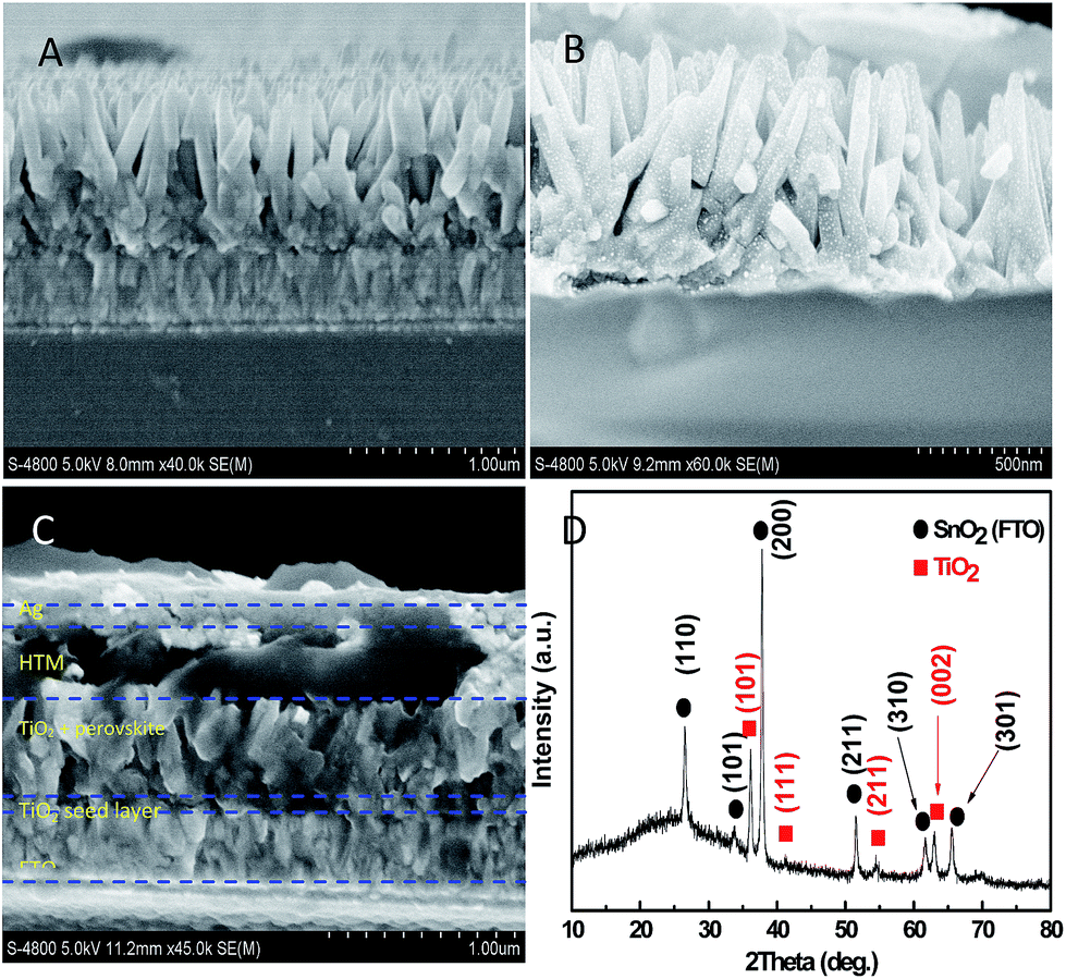 | ||
| Fig. 1 Cross-sectional FESEM images of (A) Sn-doped TiO2 nanorod grown on FTO substrate, (B) perovskite-sensitized Sn-doped TiO2 nanorod, (C) full cell; and (D) XRD as a function of 2-theta for the Sn-doped TiO2 nanorod. | ||
XRD spectrum in Fig. 1D shows vertically oriented Sn-doped TiO2 nanorod grown on FTO substrate. Except peaks of SnO2 (FTO), the other diffraction peaks coincide with the rutile TiO2 phase based on JCPDS 21-1276 standard card. Fig. 1D shows that the (101) diffraction peak intensity of rutile TiO2 is the highest of the other diffraction peaks, which is similar to the results obtained by Kim et al.34–36 Moreover, the (002) diffraction peak intensity is relatively enhanced compared to the standard card of rutile TiO2. The strongest intensity (101) peak reflects that the rutile TiO2 crystal grows with (101) plane parallel to the glass substrate.
X-ray photoelectron spectroscopy (XPS) was performed to confirm the existence and the chemical state of elements. Fig. 2A shows the Ti 2p XPS spectra of the Sn-doped TiO2 nanorod. Compared to standard binding energy of TiO2, these two peaks of Ti 2p spectra reveal a slight positive shift, which is attributed to the interaction among Ti, Sn, and O atoms.37 Moreover, the Sn 3d spectra of Sn-doped TiO2 nanorod shows a negative shift of 0.1 eV toward lower binding energy compared to the standard SnO2, which is likely boil down to the variation in electronegativity of the Ti and Sn elements (Ti = 1.54, Sn = 1.96).38 These changes confirm the formation of Ti–O–Sn structure in the Sn-doped TiO2 nanorod owing to the substitution of Ti4+ by Sn4+.
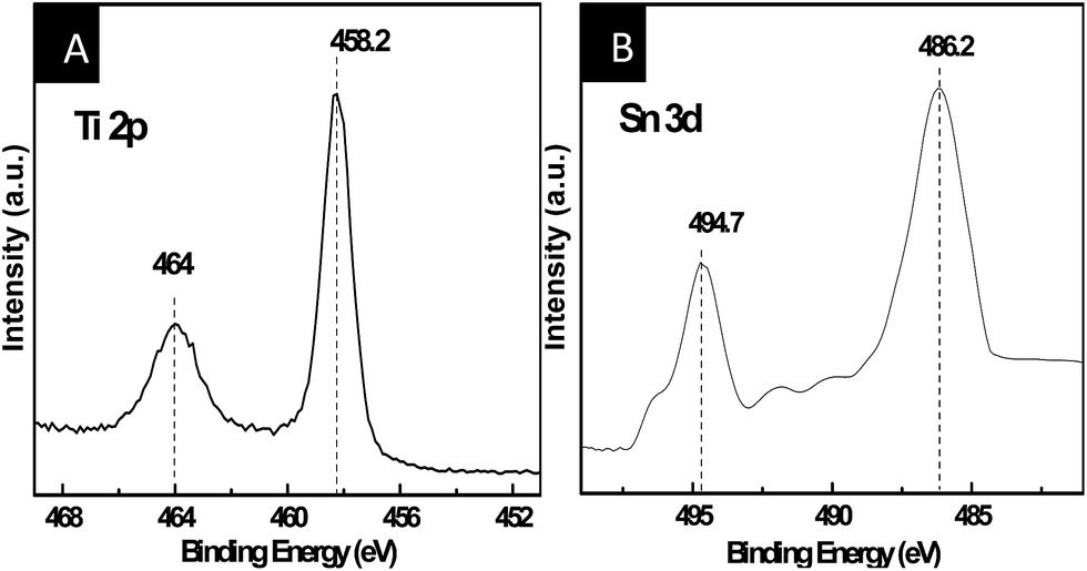 | ||
| Fig. 2 XPS spectra of (A) Ti and (B) Sn in Sn-doped TiO2 nanorod. | ||
Fig. 3A shows UV-Vis diffuse reflectance spectra of TiO2 nanorod with and without Sn doping. The reflectance spectrum of Sn-doped TiO2 nanorod is higher than that of nondoped TiO2 nanorod from 420 to 700 nm. The optical band gaps were directly obtained from the point of the extrapolation of the linear part that meeting the abscissa of Tauc plot and shown in Fig. 3B, which showed a band gap increase from 3.0 eV to 3.04 eV. The subtle change in the band gap may attribute to the substitution of Ti4+ by Sn4+.
 | ||
| Fig. 3 (A) UV-Vis diffuses reflectance spectra of TiO2 nanorods with and without Sn doping and (B) the corresponding optical bandgaps by Tauc plot. | ||
XRD diffraction spectrum in Fig. 4 shows vertically oriented Sn-doped TiO2 nanorod and CH3NH3PbI3 deposited Sn-doped TiO2 nanorod grown on FTO glass.34,35 In Fig. 4, the diffraction peaks marked with green squares represent the rutile TiO2 peaks and the peaks marked with magenta circles represent SnO2 (FTO) diffraction peaks. Other diffraction peaks correspond to the tetragonal phase CH3NH3PbI3. This indicates the successful preparation of CH3NH3PbI3 by the consumption of PbI2.10
 | ||
| Fig. 4 XRD for Sn-doped TiO2 nanorod and perovskite sensitized Sn-doped TiO2 nanorod grown on FTO glass. | ||
Fig. 5 shows the results of photoelectronic performance of doped and undoped TiO2 nanorods based solar cell. The perovskite solar cell based on Sn-doped TiO2 shows a remarkable improvement in photocurrent density and fill factor when compared to nondoped TiO2 (Fig. 5A and Table 1). Perovskite solar cell based on Sn-doped TiO2 nanorod demonstrates short-circuit current density (Jsc) of 14.88 mA cm−2, open-circuit voltage (Voc) of 0.74 V, fill factor (FF) of 0.52 and PCE of 6.31%. Thus, the higher efficiency was observed for Sn-doped TiO2. Although Voc of Sn-doped TiO2 reduced slightly (0.02 V), Jsc significantly increased from 11.26 mA cm−2 to 14.88 mA cm−2, and the FF was also improved (12% increase) for the Sn-doped TiO2 nanorod. Therefore, the PCE was improved from 3.78 to 6.31%. The external quantum efficiency (EQE) for the Sn-doped device achieving 6.31% PCE is shown in Fig. 5B (black line). The device shows higher EQE, the value of the maximum peak exceed 70%, however, the maximum peak value of nondoped TiO2 is only 56%.
 | ||
| Fig. 5 Current density–voltage (I–V) curve of perovskite solar cell based on TiO2 nanorod with and without Sn doping. (B) The external quantum efficiency of these two devices (black line: Sn-doped, red line: nondoped). | ||
| TiO2 | Jsc (mA cm−2) | Voc (V) | FF (%) | η (%) | EQE(max) |
|---|---|---|---|---|---|
| Sn-doped | 14.88 | 0.74 | 52 | 6.31 | 70% (450 nm) |
| Nondoped | 11.26 | 0.76 | 40 | 3.78 | 56% (570 nm) |
Evaluation of the EIS results helps to understand the success and failure of the device. Less internal impedance in cell suggests that the electronic transfer resistance is smaller; therefore, transport and extraction are easier. In contrast, higher value of internal impedance indicates higher electronic transfer resistance which prevents the electronic transport. Nyquist plots of two cells based on Sn-doped TiO2 nanorod and nondoped nanorod are shown in Fig. 6. The test frequency was from 1 to 100 kHz, amplitude of 5 mV. The high frequency semicircle is due to hole transport and extraction in the cathode, which represents the transport and extraction of hole and the corresponding capacitance between the interface of HTM and Ag layer. Comparison of the Sn-doped and nondoped (Fig. 6) devices reveals that the transport resistance of device based on Sn-doped TiO2 nanorod is smaller than that of the nondoped TiO2 nanorod. Small transport resistance is beneficial for the hole transfer.39 The semicircle in the middle frequency represents the synergistic effect of the recombination resistance of electron and hole and the chemical capacitance of films. Simultaneously, the series resistance (Rs) of these two cells was also observed. The value of Rs is the point of intersection between the semicircle and the X-axis in the high frequency section. The value of Rs is less than 45 Ω for the Sn-doped TiO2 nanorod device as shown in the inset of Fig. 6. However, for the nondoped device, the value of Rs increases to 170 Ω. Other sources can also contribute the improved photoelectric activity. For example, the potential difference between TiO2 and SnO2 allows electrons to easily migrate from the TiO2 surfaces to the SnO2 conduction band, which lead to decrease in the radiation combination of photoinduced electrons on the TiO2 surfaces.40 In addition, the possible formation of SnxTi1−xO2 at the interface and associated modulation of electronic properties also facilitates the electron transport through TiO2 interfaces.41
 | ||
| Fig. 6 Nyquist plots of perovskite solid-state device (black for Sn-doped and red for nondoped). | ||
Conclusions
Sn-doped TiO2 nanorod was successfully fabricated on a FTO substrate via a mild one-pot hydrothermal method. Doping of Sn changed the band gap of TiO2 material and enhances the light utilization and capture, which improved the reflectance between 420 to 700 nm. Sn-doped TiO2 nanorod was utilized in a perovskite solid state cell which yielded the PCE of 6.31%. The PCE of Sn-doped (6.31%) was almost 67% higher compared to that of nondoped TiO2 nanorod (3.78%) under the same condition. The results of EIS analysis revealed that the resistance of Sn-doped TiO2 nanorod materials was smaller than that of nondoped TiO2, thus explaining the higher PCE of cell based on Sn-doped TiO2 nanorod materials.Experimental
All the chemicals were analytical grade and used without further purification. Sn-doped TiO2 nanorods were grown on a TiO2 seed layer coated FTO substrates. The seed layers were grown on cleaned FTO glasses according to a procedure reported in the literature.32 The seed layer coated substrates were used to grow the TiO2 nanorods and to prevent direct electrical contact between FTO and HTM. Sn-doped nanorods were prepared via hydrothermal synthesis. Briefly, 20 mL hydrochloric acid (37% wt) was added into the 20 mL deionized water and stirred for about 10 min. Subsequently, Tin(IV) chloride pentahydrate (SnCl4·5H2O, 0.1 g) was added and the contents were stirred until it was completely dissolved. Tetrabutyl titanate (0.75 mL) was added and the mixture was further stirred for 30 min. Several pieces of FTO with seed layer were placed inside an 80 mL Teflon-lined stainless steel autoclave. The above mentioned mixed solution was then transferred into an autoclave, then, placed it into a 150 °C oven for 150 min. After naturally cooling, the as-formed thin film was washed with deionized water and finally dried, then calcined at 500 °C for 30 min.The perovskite sensitizer CH3NH3PbI3 was deposited on the TiO2 nanorod film by a two-step method following the reported procedure, Methylamine (32% in ethanol, 40.5 mL) and hydroiodic acid (57 wt% in water, 30 mL) were taken in a 250 mL flask and allowed to react in an ice bath for 2 h. Subsequently, the solvents were evaporated at 50 °C to produce precipitate. The precipitate was washed three times with ethyl ether and ethanol, filtrated and the product CH3NH3I was isolated. CH3NH3I solution (10 mg mL−1) was prepared by dissolving CH3NH3I in 2-propanol, and PbI2 solution 100 mM was prepared by dissolving PbI2 in γ-butyrolactone at 70 °C for 2 h.
The perovskite CH3NH3PbI3 deposition is conducted in the air with humidity around 40%. PbI2 solution was spin-coated immediately and dried at 70 °C for 30 min. After cooling, the glass was placed into CH3NH3I solution for 30 s and the film turn into black brown color. After drying at 100 °C 15 min, spiro-OMeTAD was spin-coated at 4000 rpm for 20 s. Finally, silver (Ag) was deposited using thermally evaporated on top of the device.
The cross-sectional morphologies of Sn-doped TiO2 and full cell were measured by a Hitachi S-4800 field emission scanning electron microscope (FESEM). The phases of the Sn-doped TiO2 nanorod were investigated by X-ray diffraction (XRD, SmartLab, Rigaku). Photocurrent and voltage were measured by a Keithley 2400 source meter and a solar simulator (Oriel 94023A) equipped with a 450 W xenon lamp (Newport 6279NS). The output power was adjusted to match AM 1.5 global sunlight, which was calibrated by a certified reference silicon solar cell with intensity of 100 mW cm−2 prior to use. A black aperture mask was applied to define the active area during photocurrent and voltage measurement. EIS measurement was performed with alternating current amplitude of 5 mV over the frequency range of 1 Hz to 100 kHz. Ultraviolet-Visble (UV-Vis) spectrum measurements were conducted using a Lambda 950 spectrophotometer.
Acknowledgements
This research was supported by the Natural Science Foundation of China (no. U1162108, no. 51272104); the Natural Science Foundation of Jiangsu Province Office of Education (BK20131409), Natural Science Foundation of the Jiangsu Higher Education Institutions of China (no. 11KJA150002), Qing Lan project of Jiangsu Province, the Financial Foundation of State Key Laboratory of Materials-Oriented Chemical Engineering and A Project Funded by the Priority Academic Program Development of Jiangsu Higher Education Institutions.Notes and references
- T. Moehl, M. Grätzel and J. E. Moser, Nat. Photonics, 2014, 8, 250 CrossRef.
- J. Burschka, N. Pellet, S. J. Moon, P. Gao, M. K. Nazeeruddin and M. Grätzel, Nature, 2013, 499, 316 CrossRef CAS PubMed.
- H. S. Kim, C. R. Lee, J. H. Im, K. B. Lee, T. Moehl, A. Marchioro, S. J. Moon, R. Humphry-Baker, J. H. Yum and J. E. Moser, Sci. Rep., 2012, 2, 591 Search PubMed.
- M. Grätzel and S. I. Seok, Nat. Photonics, 2013, 7, 487 Search PubMed.
- M. M. Lee, J. Teuscher, T. Miyasaka, T. N. Murakami and H. J. Snaith, Science, 2012, 338, 643 CrossRef CAS PubMed.
- J. M. Ball, M. M. Lee, A. Hey and H. J. Snaith, Energy Environ. Sci., 2013, 6, 1739 CAS.
- D. Liu and T. L. Kelly, Nat. Photonics, 2014, 8, 133 CrossRef CAS.
- D. Y. Son, J. H. Im, H. S. Kim and N. G. Park, J. Phys. Chem. C, 2014, 118, 16567 CAS.
- D. Bi, S. J. Moon, L. Häggman, G. Boschloo, L. Yang, E. M. Johansson, M. K. Nazeeruddin, M. Grätzel and A. Hagfeldt, RSC Adv., 2013, 3, 18762 RSC.
- H. S. Kim, J. W. Lee, N. Yantara, P. P. Boix, S. A. Kulkarni, S. Mhaisalkar, M. Gratzel and N. G. Park, Nano Lett., 2013, 13, 2412 CrossRef CAS PubMed.
- X. Gao, J. Li, J. Baker, Y. Hou, D. Guan, J. Chen and C. Yuan, Chem. Commun., 2014, 50, 6368 RSC.
- D. Y. Son, J. H. Im, H. S. Kim and N. G. Park, J. Phys. Chem. C, 2014, 118, 16567 CAS.
- T. Baikie, Y. Fang, J. M. Kadro, M. Schreyer, F. Wei, S. G. Mhaisalkar, M. Graetzel and T. J. White, J. Mater. Chem. A, 2013, 1, 5628 CAS.
- Z. Cheng and J. Lin, CrystEngComm, 2010, 12, 2646 RSC.
- F. Hao, C. C. Stoumpos, R. Chang and M. G. Kanatzidis, J. Am. Chem. Soc., 2014, 136, 8094 CrossRef CAS PubMed.
- Y. Kawamura, H. Mashiyama and K. Hasebe, J. Phys. Soc. Jpn., 2002, 71, 1694 CrossRef CAS.
- A. Kojima, K. Teshima, Y. Shirai and T. Miyasaka, J. Am. Chem. Soc., 2009, 131, 6050 CrossRef CAS PubMed.
- E. Edri, S. Kirmayer, D. Cahen and G. Hodes, J. Phys. Chem. Lett., 2013, 4, 897 CrossRef CAS.
- J. H. Heo, S. H. Im, J. H. Noh, T. N. Mandal, C. S. Lim, J. A. Chang, Y. H. Lee, H. j. Kim, A. Sarkar and M. K. Nazeeruddin, Nat. Photonics, 2013, 7, 486 CrossRef CAS.
- J. A. Christians, R. C. Fung and P. V. Kamat, J. Am. Chem. Soc., 2014, 136, 758 CrossRef CAS PubMed.
- H. Zhou, Q. Chen, G. Li, S. Luo, T. Song, H. Duan, Z. Hong, J. You, Y. Liu and Y. Yang, Science, 2014, 345, 542 CrossRef CAS PubMed.
- N. G. Park, J. Phys. Chem. Lett., 2013, 4, 2423 CrossRef CAS.
- A. Yella, L. P. Heiniger, P. Gao, M. K. Nazeeruddin and M. Grätzel, Nano Lett., 2014, 14, 2591 CrossRef CAS PubMed.
- S. Aharon, S. Gamliel, B. Cohen and L. Etgar, Phys. Chem. Chem. Phys., 2014, 16, 10512 RSC.
- S. Kazim, M. K. Nazeeruddin, M. Grätzel and S. Ahmad, Angew. Chem., Int. Ed., 2014, 53, 2812 CrossRef CAS PubMed.
- P. Docampo, A. Hey, S. Guldin, R. Gunning, U. Steiner and H. J. Snaith, Adv. Funct. Mater., 2012, 22, 5010 CrossRef CAS.
- S. H. Kang, S. H. Choi, M. S. Kang, J. Y. Kim, H. S. Kim, T. Hyeon and Y. E. Sung, Adv. Mater., 2008, 20, 54 CrossRef CAS.
- B. Liu and E. S. Aydil, J. Am. Chem. Soc., 2009, 131, 3985 CrossRef CAS PubMed.
- M. Yang, R. Guo, K. Kadel, Y. Liu, K. Shea, R. Bone, X. Wang, J. Heand and W. Z. Li, J. Mater. Chem. A, 2014, 2, 19616 CAS.
- C. Y. Wang, D. W. Bahnemann and J. K. Dohrmann, Chem. Commun., 2000, 1, 1539 RSC.
- F. Coloma, F. Marquez, C. Rochester and J. Anderson, Phys. Chem. Chem. Phys., 2000, 2, 5320 RSC.
- X. Chen and C. Burda, J. Am. Chem. Soc., 2008, 130, 5018 CrossRef CAS PubMed.
- C. Burda, Y. Lou, X. Chen, A. C. Samia, J. Stout and J. L. Gole, Nano Lett., 2003, 3, 1049 CrossRef CAS.
- H. Pan, J. Qian, Y. Cui, H. Xie and X. Zhou, J. Mater. Chem., 2012, 22, 6002 RSC.
- L. Liu, J. Qian, B. Li, Y. Cui, X. Zhou, X. Guo and W. Ding, Chem. Commun., 2010, 46, 2402 RSC.
- M. Liu, L. Piao, L. Zhao, S. Ju, C. Zhou and W. Wang, Chem. Commun., 2010, 46, 1664 RSC.
- Y. Duan, N. Fu, Q. Liu, Y. Fang, J. Zhang and Y. Lin, J. Phys. Chem. C, 2012, 116, 8888 CAS.
- J. Li and H. C. Zeng, J. Am. Chem. Soc., 2007, 129, 15839 CrossRef CAS PubMed.
- M. Thambidurai, J. Kim, H. Song, Y. Ko, N. Muthukumarasamy, D. Velauthapillai and C. Lee, J. Mater. Chem. A, 2014, 2, 11426 CAS.
- Z. Liu, D. D. Sun, P. Guo and J. O. Leckie, Nano Lett., 2007, 7, 1081 CrossRef CAS PubMed.
- J. Pan, S. M. Huhne, H. Shen, L. S. Xiao, P. Born, W. Mader and S. J. Mathur, J. Phys. Chem. C, 2011, 115, 17265 CAS.
Footnotes |
| † Electronic supplementary information (ESI) available. See DOI: 10.1039/c4ra11155a |
| ‡ These authors are co-first authors; they contributed equally to the work. |
| This journal is © The Royal Society of Chemistry 2014 |