DOI:
10.1039/C4RA08694E
(Paper)
RSC Adv., 2014,
4, 62132-62139
Tunable dielectric constant of polyimide–barium titanate nanocomposite materials as the gate dielectrics for organic thin film transistor applications†
Received
15th August 2014
, Accepted 12th November 2014
First published on 12th November 2014
Abstract
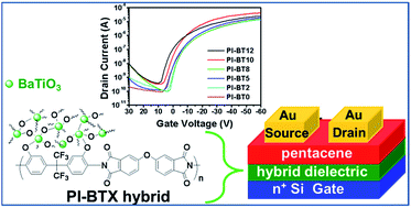
We report on a systematic study of hydroxyl-containing polyimide (PI)–BaTiO3 (BT) nanoparticle (NP) nanocomposite dielectric materials, to determine the effects of BT NPs loadings (X) for X = 0, 2, 5, 8, 10, and 12 wt%, on p-type pentacene organic thin film transistors (OTFTs). A condensation reaction to produce well-dispersed BT NPs within the PI matrix was followed by spin-coating to form a dielectric thin film directly on a silicon substrate. The thermal, optical, surface, dielectric, and electrical properties of the PI–BPX hybrid dielectric composite correlated to BT content for each sample. The hybrid dielectric composites exhibit tunable insulating properties, including high dielectric constant values in the range 5.2–11.3, high capacitances from 3.1 to 27.9 nF cm−2 for a film thickness of approximately 350 nm, and low leakage current densities in the range of 1.85 × 10⁻⁷ to 2.76 × 10⁻⁶ A cm−2 at 2 MV cm−1. Bottom-gate top-contact OTFTs fabricated using various PI–BTX hybrid dielectrics, exhibit low threshold voltages of −4.09–2.62 V, moderately high field-effect mobility rates of 3.36 × 10⁻²∼2.32 × 10⁻¹ cm2 V−1 s−1, and high ON/OFF ratios of approximately 105. This study opens a route towards transparent and highly stable hybrid dielectric materials with tunable dielectric properties, by careful selection of NPs and polymer matrix combinations.
Introduction
Organic thin film transistors (OTFTs) have attracted considerable attention for their unique features, including low fabrication cost, flexibility, and ease of processing in solution, compared to their inorganic counterparts.1–7 Much research effort has been directed at modifying OTFTs structural design to improve their performance in organic and polymeric semiconductors.8–10 Other approaches, such as controlling the deposition of crystalline organic films11–13 and controlling the nature of the interfaces present14–18 have also been developed.
In OTFTs, the interface between gate dielectric and organic semiconductor plays an important role, because charge transport is confined to a thin layer of the semiconductor close to this interface. Smoothing the dielectric surface by using a thin polymer dielectric layer can often reduce the numbers of surface traps, optimize organic semiconductor growth, and control its morphology. However, this approach has the disadvantages of reducing the dielectric constant, resulting in low capacitance and high leakage currents.19–21
Alternatively, a high dielectric constant material such as a metal oxide can induce a greater density of accumulated charge carriers in the channel region for a given electric field, but most of these are based on ceramic materials that generally require high temperature annealing processes and expensive deposition equipment.19–21 Combining organic polymer and inorganic constituents to form a hybrid insulator are an attractive strategy that can provide excellent candidates for OTFTs gates.21,22 The dielectric properties of hybrid dielectrics comprising mixtures of polymers and inorganic nanofillers, including nanoparticles (NPs), nanoclusters, and nanotubes, can be tuned by varying the type and concentration of nanofiller materials, such as by using different inorganic oxides.23–43
Polyimide (PI) is an excellent insulating material for OTFTs applications, and provides good thermal and mechanical stability.44–47 Barium titanate (BaTiO3; BT) NPs have a large dielectric constant and behave similarly to ferroelectric dielectric materials. The production of polymer–BT NPs hybrid thin films by simple solution techniques provides high quality dielectric nanocomposite materials.37,38 Polymer hybrids materials and their production method for the controlled synthesis of hybrid nanostructures were obtained from templating NPs dispersions in continuous polymeric matrix. Fine-tuning the electrical and morphological properties of gate dielectrics based on a stable PI matrix contained within high dielectric constant BT NPs can improve the performance of OTFTs devices.
To prepare solution-processable organic–inorganic hybrid gate dielectric materials for use in OTFTs devices, we synthesized and characterized a series of hybrid PI–BT nanoparticle (PI–BTX) based dielectrics, varying X (BT loading) as 0, 2, 5, 8, 10, and 12 wt% (Scheme 1). Well-dispersed BT NPs in a PI matrix were spin-coated to form hybrid dielectric films. Varying the concentration of BT NPs provides control over the dielectric properties and performance of the pentacene-based OTFTs. We show that these hybrid dielectrics are more electrically effective than neat PI (PI–BT0), and demonstrate the tailoring of dielectric properties through modification of the organic–inorganic composition. Our findings provide insight towards the development of stable transparent dielectric materials for future electronic applications.
 |
| Scheme 1 Synthetic route for PI–BTX hybrid nanocomposite dielectric thin film. | |
Experimental
Materials
2,2-Bis(3-amino-4-hydroxyphenyl)hexafluoropropane (Matrix Scientific, 98%) and 4,4-oxydiphthalic anhydride (Aldrich, 97%), barium titanate (BaTiO3, Seedchem Company PTY. LTD, 99%; particle size of ∼30 nm) were used to prepare the PI–BTX hybrid dielectric films. All solvents, including isoquinoline (95%), tetrahydrofuran (THF, 99.9%), 1-methyl-2-pyrrolidinone (NMP, 99.9%), N,N′-dimethyl acetamide (DMAc, 99.5%), and toluene (99.8%) were provided by Tedia chemicals or Acros Organics. Pentacene, used as an organic semiconductor, was purchased from TCI Co. Ltd. All chemicals and solvents were used as received, without further purification.
General procedures of polymerization
Soluble PI was prepared by the imidization of a polyamic acid (PAA) solution. First, 2,2-bis(3-amino-4-hydroxyphenyl)hexafluoro propane (0.733 g) was placed into a 100 mL three-necked round-bottom flask under nitrogen, and then 8 mL of NMP and 0.476 mL of isoquinoline were added to dissolve the reagents. Next, 4,4-oxydiphthalic anhydride (0.620 g) was slowly added with vigorous stirring. The reaction mixture was stirred for 5 h at room temperature, and then toluene (2 mL) was added to the solution. The prepared PAA solution was thermally imidized at 150 °C for a further 18 h, and then cooled to room temperature. The homogeneous 2,2-bis(3-amino-4-hydroxyphenyl) hexafluoropropane and 4,4-oxydiphthalic anhydride solution was precipitated by the addition of 300 mL of methanol. A white-gray precipitate was recovered and subsequently dried in vacuo at 60 °C for 48 h (yield: 83%).48,49
Scheme 1 shows the general reaction scheme for the preparation of the PI–BTX hybrid solutions, where “X” is a number that refers to the weight percent of BT in the hybrid materials. Taking PI–BT12 as an example, BT (0.0273 g) in 0.5 mL of DMAc was added into a 25 mL round-bottom flask. Then, PI (0.2 g) dissolved in 2 mL of DMAc was added drop wise to the solution by syringe, and the mixture stirred at room temperature for 30 min to obtain the PI–BT12 hybrid solution. To prepare the PI–BT12 hybrid thin film, the precursor PI–BT12 solution was filtered and spin-coated onto a silicon wafer at 2000 rpm for 20 s. The resulting hybrid dielectric film was soft-baked at 60 °C for 20 min, 100 °C for 20 min, then at 150 °C for 1 h.
Characterization
Fourier transformed infrared (FTIR) spectra of the prepared PI–BTX hybrid thin films were acquired using on using a PerkinElmer Spectrum One spectrophotometer. In situ Raman spectroscopy was performed to determine and compare the phase transition temperatures using a Renishaw Invia Raman microscope over a wavenumber range of 150–1000 cm−1 and temperature from 25 to 300 °C. The thermal properties of the PI–BTX hybrids were assessed using a TA Instruments Q50 thermogravimetric analysis (TGA) instrument and Q20/RSC90 differential scanning calorimeter (DSC) at heating rates of 20 and 10 °C min−1, respectively. Contact-angle analysis was performed using an optical contact-angle apparatus with data acquisition software. The transmittances of the hybrid films coated on the quartz substrates were collected using a Jasco V-650 UV/Vis/NIR spectrophotometer. XRD analysis was performed on a PANalytical X'Pert PRO MPD X-ray diffractometer using CuKα radiation. The morphologies of thin films were observed by a high-resolution transmission electron microscope (HRTEM; JEOL, JEM-2100), a scanning electron microscope (SEM; Hitachi H-2400), and an atomic force microscope (AFM; Veeco DI 3100). The thicknesses of the PI–BTX hybrid thin films were analyzed by profilometry (ET-4000, Kosaka Laboratory Ltd).
OTFTs fabrication and characterization
OTFTs were fabricated on Si substrates using bottom-gate top-contact (BGTC) architecture. Heavily doped n+ Si substrates were cleaned with deionized water, acetone, and isopropanol in an ultrasonic bath. After deposition of the hybrid dielectric layer (∼350 nm), the pentacene active layer (∼50 nm) was fabricated by thermal evaporation deposition at the pressure of approximately 10−7 Torr and deposition rate of 0.5 Å s−1. Finally, Au source and drain electrodes were deposited on the active semiconducting layer by vacuum thermal evaporation, to provide source-drain contacts of length (L) = 50 μm and width (W) = 1000 μm. For the metal/insulator/metal (MIM) test structures, 0.6 mm diameter A1 electrodes were deposited directly onto the gate hybrid dielectric/Si films by shadow masking. MIM direct current measurements and OTFTs measurements were performed under ambient conditions using a probe station interface with an Agilent E4980A precision LCR meter (10 kHz to 1 MHz), and Agilent B1500A semiconductor device parameter analyzer.
Results and discussion
PI–BTX hybrid dielectric film fabrication and characterization
The PI–BTX hybrid materials provided the gate dielectric for OTFTs devices. PI is well suited for use as the insulating matrix because of its high thermal and environmental stability and easy chemical modification. We performed two-step polymerization process of PI, involving polyamic acid synthesis and chemical imidization. Hybrid thin films were prepared by spin coating a solution of the appropriate precursor followed by thermal curing, as described in the Experimental section. Thermal treatment results in the formation of links between the prepared functionalized PI via its pendent hydroxyl groups, to the surface-modified BT NPs filler material. The dispersion and aggregation behaviors of the NPs determine the dielectric and film properties of PI–BTX hybrids. The combination of high dielectric constant guest fillers with a stable polymer host can provide solution-processable PI–BTX dielectric materials.
We studied the influence of composition on the structure and properties of dielectric films comprising a purely inorganic BT phase, polymeric material, and inorganic and polymer hybrid components, present in various weight ratios. Three main spectral features of BT ceramics detected by Raman spectroscopy (Fig. 1(a)) at 25 °C are: (1) An intense broad band appearing at 508 cm−1 [A1 (TO)], (2) a broad, weak band at 711 cm−1 [A1 (LO)], and (3) a sharp band at 306 cm−1 [B1, E(TO + LO)], indicating that BT NPs possess coexisting rhombohedral and orthorhombic phases similar to that described in a previous report.50 The structures of treated PI–BTX nanocomposite films were examined by a combination of Raman and FTIR spectroscopies. Fig. 1(a) shows Raman spectra of pure BT, PI (PI–BT0) and several PI–BTX hybrids (PI–BT2, PI–BT5, PI–BT8, PI–BT10, and PI–BT12). The three main BT absorption bands were also present in the spectra of the PI–BTX hybrids. The intensity of these characteristic BT bands increases with BT concentration. Fig. 1(b) and S1 of ESI† show the FTIR spectra for pure BT and for PI–BTX hybrids with various compositions, respectively. Pure PI (PI–BT0) is identifiable during the complete PAA polycyclic-dehydration process, by imide C
O stretching bands at 1788 cm−1 and a C–N–C stretching absorption at 1370 cm−1 and absence of C
O from amid acid at 1680 cm−1. The intense peaks around 3000 cm−1 are attributed to the hydroxyl (–OH) stretching from the side chain of PI, and the intensity of this band is slightly decreased in FTIR spectra when more BT NPs are covalently bonded with PI (from PI–BT0 to PI–BT12). The strong and broad absorption band at approximately 500–700 cm−1 in both figures arises from Ti–O stretching vibrations in BT NPs. The PI–BTX hybrid FTIR spectra are consistent with the presence of both rhombohedral and orthorhombic morphologies. The greater the ratio of the BT in the hybrid sample, the greater the intensity of the Ti–O band appears in the low wavenumber region (500–700 cm−1). The intensity of both Raman and FTIR spectra is proportional in part, to the number of contributing bonds present, thus, these spectra indicate that the introduction of BT nanofillers into the PI matrix results in the formation of PI–BTX hybrids. This evidence also supports the proposed hybrid formation process, in which increases in the numbers of BT moieties in the system results in larger and more numerous BT regions.
 |
| Fig. 1 (a) Raman spectra and (b) FTIR spectra of PI–BTX hybrid nanocomposite thin films. | |
The SEM image in Fig. S2 of ESI† and the AFM image in Fig. 2 show that spin coating of PI and BT NPs mixtures produce smooth and robust PI–BTX dielectric films at low temperature. SEM imaging of the hybrid surface demonstrates that the binding compatibility between PI and BT NPs on Si substrate facilitates the formation of uniform large-scale thin films with homogenous NP distributions, in OTFTs dielectric materials. The tapping-mode AFM height image of the dielectric layer (Fig. 2) reveals that the root-mean-square (rms) roughness values for 2 × 2 μm regions in the PI–BTX dielectric are in the range 0.475–11.924 nm. These AFM images of the hybrid PI–BTX samples show how surface morphology depends on the theoretical BT loading content in the hybrid material. Increases in the BT content of the PI matrix appears to result in increased surface rms roughness. However, all of the hybrid dielectric samples presented pinhole-free surfaces. Overall, our observations suggest that BT nanoparticles effectively disperse in the hybrid dielectric film PI matrix.
 |
| Fig. 2 AFM images dielectric surfaces: (a) PI–BT0, (b) PI–BT2, (c) PI–BT5, (d) PI–BT8, (e) PI–BT10, and (f) PI–BT12. | |
The XRD results (Fig. 3) for the sintered BT sample show the formation of a BT perovskite phase. We assigned the sharp X-ray reflections at 2θ = 23.6°, 32.7°, 40.5°, 46.1°, 52.3°, and 56.5° to (100), (110), (111), (200), (210) and (211) planes, respectively.51 No other diffraction peaks related to BT or significant crystalline phases were present. With the exception of PI–BT12, the PI–BTX thin films only produced broad bands in the XRD spectra, indicating an amorphous structure for BT loadings up to 10%, regardless of the BT hybrid precursor BTX hybrid mixtures, as determined by TGA and DSC. All the thermal properties were summarized in Table 1. The content Fig. S3 of ESI† shows the thermal behaviors of PI-decomposition temperature, defined as the temperature at which 5% loss of mass occurs, increases with increasing BT loading content. For pure PI (PI–BT0) and low BT concentrations (PI–BT2), we attributed the abrupt weight loss to a hydroxyl group, which remained unreacted during the condensation process at low BT content. A degradation observed at approximately 500 °C results from decomposition of the aromatic PI moiety. Sample residues seen in the high temperature region (approx. 800 °C) correlate linearly with the amount of BT incorporated within the PI matrix. The addition of inorganic BT enhances the composite material's thermal stability, for both decomposition temperature and glass transition temperature, suggesting that presence of the inorganic component limits segmental motion, by forming O–BT–O bonds.
 |
| Fig. 3 XRD result for BT and PI–BTX samples. | |
Table 1 Summary of dielectric and film properties for PI–BTX hybrid dielectric film
Dielectric materials |
Thickness [nm] |
Td [oC] |
Tg [oC] |
Water contact angle [°] |
Diidomethane contact angle [°] |
Surface energy [mJ m−2] |
RMS roughness [nm] |
PI–BT0 |
351 |
410 |
280 |
63.4 |
31.1 |
48.1 |
0.475 |
PI–BT2 |
360 |
439 |
302 |
63.6 |
31.3 |
48.0 |
4.147 |
PI–BT5 |
362 |
464 |
315 |
64.3 |
34.2 |
46.8 |
6.675 |
PI–BT8 |
355 |
469 |
326 |
66.7 |
37.6 |
44.8 |
8.684 |
PI–BT10 |
364 |
482 |
348 |
73.7 |
49.2 |
37.9 |
8.943 |
PI–BT12 |
358 |
493 |
352 |
83.5 |
39.8 |
39.8 |
11.924 |
Fig. 4 shows the transmittances of coated hybrid dielectric films over the entire visible region. Even at high BT loading concentration, all of the PI–BTX hybrid dielectric materials exhibit good transmittance (greater than 85% at 500 nm), and are colorless. These properties are beneficial for applications that require transparency such as by a transistor passivation layer used in a high resolution and brightness electronic display. The superior transparency of the PI–BTX hybrid may result from the reduced formation of charge transfer complexes, and limited electronic conjugation along the PI backbone, that arise from the presence of fluorine moieties, the non-coplanar PI geometry, and from the bulky BT substituents present in PI the side chains.52
 |
| Fig. 4 Optical transmittance spectra of PI–BTX hybrid nanocomposite thin films. | |
OTFTs characteristics with PI–BTX hybrids as dielectric
The dielectric properties of the PI–BTX films are strongly dependent on BT content. The MIM capacitor device used for quantitative leakage current/capacitance measurements (Fig. 5) contains various PI–BTX hybrid dielectric layers sandwiched between two Al electrodes. Fig. 5(a) shows leakage current densities for the PI–BTX hybrid gate dielectric films fabricated on Si substrate, with various BT contents, as a function of an applied field. At a field strength of −2 MV cm−1, the of PI–BTX hybrid film leakage current densities are in the range of 1.85 × 10⁻⁷–2.76 × 10⁻⁶ A cm−2, slightly greater than that for pure PI film (1.17 × 10⁻⁷ A cm−2). Thus, the dielectric properties of these hybrid insulators are suitable for the fabrication of highly stable OTFTs. Fig. 5(b) shows a capacitance (C)-frequency (F) plot for a MIM structure fabricated using PI–BTX dielectrics, for various BT loadings. The figure reveals that increasing BT content effectively enhances the hybrid film's capacitance for a given dielectric thickness. PI–BTX hybrid capacitances in the range of 13.1–27.9 nF cm−2 at 10 kHz are readily obtainable, and are much greater than the capacitances of a 350 nm-thick SiO2 layer or of pure PI (PI–BT0) film (∼9.7 nF cm−1). An observed linear correlation between BT loading and frequency response was flat over the range 10 kHz–1 MHz. At lower frequencies, the capacitance increases slightly, possibly because of increase in the response time available for polarization. The dielectric constants (k) were evaluated using the following equation: |
 | (1) |
where, C is the measured capacitance, ε0 is the permittivity of free space, A is the area of the capacitance, and d is the thickness of dielectric layer. Table 2 summarizes the dielectric constants detected at 10 kHz. The measured dielectric constant values for the hybrid materials ranged from 3.9 for PI–BT0 to 5.2, 6.8, 8.0, 9.8, and 11.3 for PI–BT2, PI–BT5, PI–BT8, PI–BT10, and PI–BT12, respectively. The dielectric constant for the hybrid dielectric at 12 wt% is about three times that of pristine PI–BT0, but it does not induce strong phase separation. The hybrid materials' dielectric constant can be raised by increasing the inorganic BT NPs content; the dielectric constant increases with BT NPs content, because of the higher dielectric permittivity of the well-dispersed nanofiller, isolated by the passivating layers of polymer matrix. The BT NPs present in the PI precursor solution undergo a condensation reaction to form the –O–BT–O– network interface that sterically hinders the movement of BT NPs, resulting in the uniform incorporation of BT NPs in the PI phase. The use of this high dielectric constant inorganic nanomaterial within the PI film affords a greater charge density at the interface, and a smooth surface morphology that minimizes current leakage, facilitated by use of sufficiently thick insulators.
 |
| Fig. 5 (a) Leakage characteristics and (b) capacitance vs. frequency plots for the PI–BTX hybrid dielectrics. | |
Table 2 Summary of electrical parameters for MIM device and pentacene OTFTs based on different PI–BTX hybrid dielectrics
Dielectric materials |
Leakage current densitya [A cm−2] |
Capacitanceb [nF cm−2] |
Dielectric constantb [—] |
μ [cm2 V−1 s−1] |
Vt [V] |
ION/IOFF [—] |
At −2 MV cm−2. At 10 kHz. |
PI–BT0 |
1.17 × 10⁻⁷ |
9.7 |
3.9 |
3.95 × 10⁻² |
−3.4 |
1.3 × 10⁵ |
PI–BT2 |
1.85 × 10⁻⁷ |
13.1 |
5.2 |
3.36 × 10⁻² |
−4.1 |
1.1 × 10⁵ |
PI–BT5 |
5.04 × 10⁻⁷ |
17.0 |
6.8 |
5.38 × 10⁻² |
−3.7 |
1.5 × 10⁵ |
PI–BT8 |
7.27 × 10⁻⁷ |
19.6 |
8.0 |
5.43 × 10⁻² |
−4.1 |
1.7 × 10⁵ |
PI–BT10 |
9.89 × 10⁻⁷ |
24.1 |
9.8 |
2.32 × 10⁻¹ |
−0.5 |
1.8 × 10⁵ |
PI–BT12 |
2.76 × 10⁻⁶ |
27.9 |
11.3 |
6.38 × 10⁻² |
2.6 |
6.7 × 10⁴ |
Thus, we prepared hybrid films for OTFTs applications, while exercising control over the film's dielectric constant. BGTC pentacene OTFTs were fabricated, using PI–BTX hybrid films as the gate dielectric. From the accumulated-mode output plots (Fig. S4 of ESI†), all the devices exhibit typical p-type OTFTs behaviors, suggesting that the majority of transporting carriers in the channel are holes. We determined the field-effect mobility (μ) from the transfer curves, by applying the eqn (2) to the saturation region.
|
 | (2) |
where,
Id is the drain current,
Vt is threshold voltage,
W and
L are the channel width and length respectively, and
Ci is the capacitance per unit area of the hybrid gate dielectric. The average field-effect mobility is calculated by plotting the square root of
Id against
Vg.
Fig. 6 shows a representative transfer plot for OTFTs fabricated using
PI–BTX as the dielectric. The OTFTs performance characteristics for these devices as a function of BT concentration are collected in
Table 2. All of these hybrid dielectrics films are quite smooth, and thus device performance is both reproducible and reliable. Devices using the neat polyimide dielectric,
PI–BT0, have a hole mobility of 3.95 × 10
−2 cm
2 V
−1 s
−1, which approaches previously reported values for pentacene-based OTFTs with other PI materials, and that reported for use of conventional SiO
2 as the gate dielectric.
44–47 Greater hole mobility is obtainable for OTFTs with a larger BT loading concentration, mainly because of increased capacitance, which facilitates the accumulation of charge carriers in the channel. Here, the
PI–BT10 dielectric provides the greatest observed mobility of 2.32 × 10
−1 cm
2 V
−1 s
−1. However, an excess of BT sites disrupt the deposition of pentacene, as seen for the
PI–BT12 dielectric based device. Relatively high OTFTs ON/OFF current ratios, of approximately 10
5 are observed for all samples. Interestingly, all the threshold voltages are quite small, even for the neat PIs and samples with low BT loadings; however,
PI–BT12 devices exhibit a more positive threshold voltage. The use of large capacitance hybrid dielectrics is beneficial for reducing threshold voltage, even to a threshold voltage of 0 V, compared to transistor fabricated OTFTs using SiO
2 with a similar thickness. The threshold voltages of OTFTs with
PI–BTX hybrid dielectrics are not significantly altered; it is possible that the prepared hybrid dielectric can annihilate major charge traps during the condensation reaction process. Compared with the
PI–BT0 dielectric, the electrical hysteresis behavior of
PI–BT12 shows a small change when the gate voltage is swept continuously from 20 to −60 V and then returned to 20 V (
Fig. 7). The small hysteresis arises from the unreacted hydroxyl groups that remain in the hybrid gate dielectric.
53 In general, OTFTs exhibit moderately high mobility (>10
−1 cm
2 V
−1 s
−1), have an acceptable ON/OFF current ratio of approximately 10
5, and operate at low threshold voltages, close to 0 V, if the hybrid dielectric capacitance is increased by incorporating BT at concentrations up to 10 wt%.
 |
| Fig. 6 Transfer characteristics of OTFTs based on various PI–BTX hybrid dielectric layers. | |
 |
| Fig. 7 Dual sweep (forward and backward sweep) transfer characteristics of OTFTs based on PI–BT0 and PI–BT12 hybrid dielectric layers. | |
Fig. S5 and S6 of ESI† show contact angle measurements for the surfaces of the PI–BTX hybrid dielectric materials. We quantified the surface energies of the hybrid gate dielectric by calculation, based on the different polarities of deionized (DI) water and diiodomethane.54 Table 1 shows contact angle data and surface energies for the PI–BTX hybrid dielectrics. A low contact angle at the solid surface contact with a water drop means that the surface is hydrophilic with a large surface energy, while a large contact angle suggests a hydrophobic surface with low surface energy.54 The PI–BT0 polymeric film, which lacks added BT, exhibits a small water contact angle of 63.4°. However, hybrid gate dielectrics that incorporated BT show increasing contact angles as the BT content increases. We explain this observation by the fewer hydroxyl groups that are present at greater BT concentrations, because of the condensation reaction between functional PI and the modified BT NPs. Our results also confirm that surface energy reduces to 37.9 mJ m−2 upon in the presence of 10 wt% BT. High dielectric constant BT NPs are surrounded by the low dielectric constant PI matrix, which reduces the NPs surface energy. In most cases, a dielectric surface with low surface energy and high water contact angle provides sites for organic semiconductor chain growth.55
We characterized the morphologies of pentacene thin films grown on PI–BTX hybrid dielectrics by AFM (Fig. 8). Pentacene is inherently hydrophobic, and the PI–BT10 insulator is better matched to the pentacene surface energy and is generally compatible with pentacene growth. The size of pentacene grain domains deposited on hybrid dielectrics increases with BT content in the PI–BTX hybrids, thus, the affinity of the dielectric surface for pentacene determines the semiconductor growth rates, and the BT mobility within the OTFTs device (Tables 1 and 2).56 Reductions in grain size or in the grain boundary between crystallites correlate with the numbers of interfacial trapping sites that may disrupt charge transport. Grain size and charge mobility increase with BT content, from PI–BT0 to PI–BT10. The enhanced mobility observed in pentacene OTFTs based on the PI–BT10 dielectric demonstrate an efficient charge transport process, because of well-connected domains, without significant charge hopping across grain boundaries and without disordered domains. Insertion of the high dielectric constant hybrid film induces the formation of greater charge carrier densities at the dielectric/semiconductor interface, and thus, improves OTFTs performance because of the resulting improvements in mobility and threshold voltage. However, as the concentration of BT content increases further to 12 wt%, device mobility falls. The rougher morphology of the PI–BT12 surface, with its aggregates of BT particles, features traps close to the interface, causing significant interference with the formation of crystalline structures. The greater boundary concentration of small aggregated domains in PI–BT12 restricts charge transport in the semiconductor channel.
 |
| Fig. 8 AFM images of pentacene deposited on dielectric: (a) PI–BT0, (b) PI–BT2, (c) PI–BT4, (d) PI–BT8, (e) PI–BT10, and (f) PI–BT12. | |
In this study, nanocomposite dielectrics composed of PI, with a large fraction of homogenously dispersed large dielectric constant surface-functionalized BT NPs are compared to previously reported direct PI blended nanocomposite materials that do not contain any reactive sites for NPs in their PI matrices.40–42 Our solution-processable hybrid dielectrics produce improved OTFTs characteristics because of an optimized combination of high dielectric constant inorganic oxide NPs and host PI matrix.
Conclusions
In conclusion, a series of novel high dielectric constant PI–BTX hybrid thin films with different inorganic loadings were successfully fabricated for use as a dielectric material in OTFTs. The polymer-inorganic hybrid materials featured a covalently bonded interface, and revealed a high degree of dispersion of BT NPs in the PI matrix. The dielectric constant for the composite material was tunable by varying the weight percent of BT NPs incorporated into the PI matrix, providing significant improvements in the dielectric properties. The device performance (mobility and threshold voltage), and film properties (dielectric constant, morphology, and hydrophilicity/hydrophobicity) showed a strong correlation with BT concentration. These findings suggest that PI–BTX hybrid films can be tailored to meet the requirements of practical applications. Additionally, our PI hybrid materials illustrate a new approach towards the development of transparent, high thermal stability, and environmental safe gate dielectrics for application in the field of transistors and related electronic devices.
Acknowledgements
The authors gratefully acknowledge the financial support provided by the Ministry of Science and Technology of Taiwan (NSC 101-2221-E-131-006-MY3 & 101-2218-E-008-010-MY3).
References
- S. Allard, M. Forster, B. Souharce, H. Thiem and U. Scherf, Angew. Chem., Int. Ed., 2008, 47, 4070 CrossRef CAS PubMed.
- H. Dong, L. Jiang and W. Hu, Phys. Chem. Chem. Phys., 2011, 13, 6286 RSC.
- Y. Guo, G. Yu and Y. Liu, Adv. Mater., 2010, 22, 4427 CrossRef CAS PubMed.
- H. N. Tsao and K. Müllen, Chem. Soc. Rev., 2010, 39, 2372 RSC.
- A. Facchetti, Chem. Mater., 2011, 23, 733 CrossRef CAS.
- J. Sun, B. Zhang and H. E. Katz, Adv. Funct. Mater., 2011, 21, 29 CrossRef CAS.
- C.-a. Dai, F. Zhang and D. Zhu, Adv. Mater., 2013, 25, 313 CrossRef PubMed.
- A. R. Murphy and J. M. J. Fréchet, Chem. Rev., 2007, 107, 1066 CrossRef CAS PubMed.
- C. Wang, H. Dong, W. Hu, Y. Liu and D. Zhu, Chem. Rev., 2012, 112, 2208 CrossRef CAS PubMed.
- J. Mei, Y. Diao, A. L. Appleton, L. Fang and Z. Bao, J. Am. Chem. Soc., 2013, 135, 6724 CrossRef CAS PubMed.
- S. Liu, W. M. Wang, A. L. Briseno, S. C. B. Mannsfeld and Z. Bao, Adv. Mater., 2009, 21, 1217 CrossRef CAS.
- A. A. Virkar, S. Mannsfeld, Z. Bao and N. Stingelin, Adv. Mater., 2010, 22, 3857 CrossRef CAS PubMed.
- Y. Wen, Y. Liu, Y. Guo, G. Yu and W. Hu, Chem. Rev., 2011, 111, 3358 CrossRef CAS PubMed.
- Y. D. Park, J. A. Lim, H. S. Lee and K. Cho, Mater. Today, 2007, 10, 46 CrossRef CAS.
- S. A. DiBenedetto, A. Facchetti, M. A. Ratner and T. J. Marks, Adv. Mater., 2009, 21, 1407 CrossRef CAS.
- C.-a. Dai, Y. Liu, G. Yu and D. Zhu, Acc. Chem. Res., 2009, 42, 1573 CrossRef PubMed.
- H. Wang and D. Yan, NPG Asia Mater., 2010, 2, 69 CrossRef.
- H. Ma, O. Acton, D. O. Hutchins, N. Cernetic and A. K.-Y. Jen, Phys. Chem. Chem. Phys., 2012, 14, 14110 RSC.
- J. Veres, S. Ogier and G. Lloyd, Chem. Mater., 2004, 16, 4543 CrossRef CAS.
- A. Facchetti, M.-H. Yoon and T. J. Marks, Adv. Mater., 2005, 17, 1705 CrossRef CAS.
- R. P. Ortiz, A. Facchetti and T. J. Marks, Chem. Rev., 2010, 110, 205 CrossRef CAS PubMed.
- S. Gross, D. Camozzo, V. D. Noto, L. Armelao and E. Tondello, Eur. Polym. J., 2007, 43, 673 CrossRef CAS PubMed.
- F.-C. Chen, C.-W. Chu, J. He, Y. Yang and J.-L. Lin, Appl. Phys. Lett., 2004, 85, 3295 CrossRef CAS PubMed.
- S. Jeong, D. Kim, S. Lee, B.-K. Park and J. Moon, Appl. Phys. Lett., 2006, 89, 092101 CrossRef PubMed.
- C. Jung, A. Maliakai, A. Sidorenko and T. Siegrist, Appl. Phys. Lett., 2007, 90, 062111 CrossRef PubMed.
- S. Jeong, S. Lee, D. Kim, H. Shin and J. Moon, J. Phys. Chem. C, 2007, 111, 16083 CAS.
- S. Jeong, D. Kim and J. Moon, J. Phys. Chem. C, 2008, 112, 5245 CAS.
- S. Lee, S. Jeong and J. Moon, Org. Electron., 2009, 10, 982 CrossRef CAS PubMed.
- Y. Gan, Q. J. Cai, C. M. Li, H. B. Yang, Z. S. Lu, C. Gong and M. B. Chan-Park, ACS Appl. Mater. Interfaces, 2009, 1, 2230 CAS.
- Y.-g. Ha, S. Jeong, J. Wu, M.-G. Kim, V. P. Dravid, A. Facchetti and T. J. Marks, J. Am. Chem. Soc., 2010, 132, 17426 CrossRef CAS PubMed.
- J. Kim, S. H. Lim and Y. S. Kim, J. Am. Chem. Soc., 2010, 132, 14721 CrossRef CAS PubMed.
- L. Li, W. Hu, L. Chi and H. Fuchs, J. Phys. Chem. B, 2010, 114, 5315 CrossRef CAS PubMed.
- N. T. Tien, T. Q. Trung, Y. G. Seoul, D. I. Kim and N.-E. Lee, ACS Nano, 2011, 5, 7069 CrossRef PubMed.
- Y. Wang and H. Kim, Org. Electron., 2012, 13, 2997 CrossRef CAS PubMed.
- Y. Zhou, S.-T. Han, Z.-X. Xu and V. A. L. Roy, J. Mater. Chem., 2012, 22, 4060 RSC.
- Y. Zhou, S.-T. Han, Z.-X. Xu, X.-B. Yang, H.-P. Ng, L.-B. Huang and V. A. L. Roy, J. Mater. Chem., 2012, 22, 14246 RSC.
- R. Schroeder, L. A. Majewski and M. Grell, Adv. Mater., 2005, 17, 1535 CrossRef CAS.
- P. Kim, S. C. Jones, P. J. Hotchkiss, J. N. Haddock, B. Kippelen, S. R. Marder and J. W. Perry, Adv. Mater., 2007, 19, 1001 CrossRef CAS.
- P. Kim, X. H. Zhang, B. Domercq, S. C. Jones, P. J. Hotchkiss, S. R. Marder, B. Kippelen and J. Perry, Appl. Phys. Lett., 2008, 93, 013302 CrossRef PubMed.
- W.-H. Lee, C. C. Wang, W.-T. Chen and J.-C. Ho, Jpn. J. Appl. Phys., 2008, 47, 8955 CrossRef CAS.
- W.-H. Lee and C. C. Wang, J. Vac. Sci. Technol., B: Microelectron. Nanometer Struct.--Process., Meas., Phenom., 2009, 27, 1116 CrossRef CAS.
- W.-H. Lee, C. C. Wang and S. D. Liu, J. Nanosci. Nanotechnol., 2011, 11, 1968 CrossRef CAS PubMed.
- L. H. Chen, P. Lin, J. C. Ho, C. C. Lee, C. Kim and M. C. Chen, Synth. Met., 2011, 161, 1527 CrossRef CAS PubMed.
- Y. Kato, S. Iba, R. Teramoto, T. Sekitani, T. Someya, H. Kawaguchi and T. Sakurai, Appl. Phys. Lett., 2004, 84, 3789 CrossRef CAS PubMed.
- S. Y. Yang, S. H. Kim, K. Shin, H. Jeon and C. E. Park, Appl. Phys. Lett., 2006, 88, 173507 CrossRef PubMed.
- S. Pyo, Y. Lee, J. Jeon, M. H. Yi and S.-K. Kwon, J. Appl. Phys., 2006, 99, 073711 CrossRef PubMed.
- T. Sekitani, T. Someya and T. Sakurai, J. Appl. Phys., 2006, 100, 024513 CrossRef PubMed.
- G.-S. Liou, P.-H. Lin, H.-J. Yen, Y.-Y. Yu and W.-C. Chen, J. Polym. Sci., Part A: Polym. Chem., 2010, 48, 1433 CrossRef CAS.
- G.-S. Liou, P.-H. Lin, H.-J. Yen, Y.-Y. Yu, T.-W. Tsai and W.-C. Chen, J. Mater. Chem., 2010, 20, 531 RSC.
- V. Torres-Heredia, J. Muñoz-Saldaña, F. J. Espinoza Beltrán, A. Márquez Herrera and A. Zapata Navarro, Adv. Technol. Mater. Mater. Process. J., 2005, 7, 105 CAS.
- S. H. Choi, I. D. Kim, J. M. Hong, K. H. Park and S. G. Oh, Mater. Lett., 2007, 61, 2478 CrossRef CAS PubMed.
- Y.-W. Wang and W.-C. Chen, Mater. Chem. Phys., 2011, 126, 24 CrossRef CAS PubMed.
- S. Lee, B. Koo, J. Shin, E. Lee, H. Park and H. Kim, Appl. Phys. Lett., 2006, 88, 162109 CrossRef PubMed.
- A. J. Kinloch, Adhesion and adhesives: science and technology, Chapman & Hall, 1987, pp. 24–38 Search PubMed.
- W. Y. Chou, C.-W. Kuo, H.-L. Cheng, Y.-R. Chen, F.-C. Tang, F.-Y. Yang, D.-Y. Shu and C.-C. Liao, Appl. Phys. Lett., 2006, 89, 112126 CrossRef PubMed.
- C. Kim, A. Facchetti and T. J. Marks, Science, 2007, 318, 76 CrossRef CAS PubMed.
Footnote |
† Electronic supplementary information (ESI) available. See DOI: 10.1039/c4ra08694e |
|
This journal is © The Royal Society of Chemistry 2014 |
Click here to see how this site uses Cookies. View our privacy policy here.