Investigations on structural and optical properties of ZnO and ZnO:Co nanoparticles under dense electronic excitations

Shiv Kumara, Kandasami Asokanb, Ranjan Kumar Singha, Sandip Chatterjeec, Dinakar Kanjilalb and Anup Kumar Ghosh*a
aMaterials Research Lab. Department of Physics, Banaras Hindu University, Varanasi 221 005, India. E-mail: akghosh@bhu.ac.in; anupkg66@gmail.com
bInter University Accelerator Centre, Aruna Asaf Ali Marg, New Delhi 110 067, India
cDepartment of Applied Physics, Indian Institute of Technology, Banaras Hindu University, Varanasi 221 005, India

Received 6th September 2014 , Accepted 7th November 2014

First published on 12th November 2014


Abstract

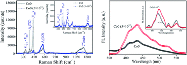
In the present study, the structural, morphological, and optical properties of Co-doped ZnO nanoparticles (NPs) prepared by a sol–gel method before and after dense electronic excitations caused by swift heavy ion irradiation have been reported. The pristine and ZnO:Co NPs were irradiated by using a 200 MeV Ag15+ ion beam at a fluence of 5 × 10¹² ions per cm2. Structural characterization has been performed using X-ray diffraction (XRD) with Rietveld refinement. It shows that the samples are of single phase; grain size and tensile strain has been increased in the ion-irradiated samples. Room temperature Raman spectroscopy measurements show that microscopic structural disorders reduce the translational symmetry giving rise to local distortions in the lattice. Atomic force microscopic (AFM) studies show prominent grain boundaries and suggest that roughness of the irradiated surfaces increases strongly compared to their pristine counterparts. Optical absorption and photoluminescence (PL) studies also reflect the dopant incorporation and swift heavy ion (SHI) irradiation effect on the nanoparticles. UV-Vis absorption measurement has been utilized to estimate the optical bandgap of pristine and irradiated ZnO and Co-doped ZnO nanoparticles. Enhancement in the PL intensity has been observed in the irradiated samples with respect to their pristine counterparts which can be explained on the basis of the increase of different defect states and Zn–O bonds on the surfaces of the irradiated nanoparticles arising from surface modification. Grain boundaries have played an important role in the optical properties (absorption and PL).


Introduction

Diluted magnetic semiconductors (DMSs)1 are compounds in which a very small fraction of non-magnetic ions is replaced by magnetic ions (typically transition metal (TM) ions such as Fe, Mn, Co etc. and rare earth metal ions). In DMSs magnetic ions are randomly distributed and show typical semiconductor behaviour as well as pronounced magnetic properties. The most important feature of DMSs are the co-existence and interaction of two different electronic subsystems namely delocalized conduction band (s-type) and valence band (p-type) electrons and localized (d- or f-type) electrons of magnetic ions.1 The applicability of DMSs has been limited due to the very low value of the Curie temperature (Tc ∼ 170 K). The realization of DMSs having a Curie temperature above room temperature will potentially lead to a new generation of spintronics devices with revolutionary electrical and optical properties.

Theoretical calculations, based on Zener model of magnetism with holes mediated exchange interaction, predicted the possibility of room temperature ferromagnetism in TM doped ZnO (II–VI) and GaN (III–V) or more generally in wide band gap semiconductors.2 In the past decades, ZnO-based DMSs1 are considered to be one of the most promising materials for ultraviolet LEDs,3 laser diodes, spintronics and many other spin-based devices4,5 because of its large band gap (3.36 eV) and high exciton binding energy (60 meV). ZnO is an optically transparent II–VI semiconductor and well-known piezoelectric and electro-optic material having hexagonal wurtzite structure with C6v4 (P63mc) space group. Studies of different physical properties (such as structural, optical, magnetic properties etc.) based on different TM (such as Cr, Mn, Fe, Co etc.) doped ZnO have been explored by various researchers.6–11 Doping of semiconductor with TM elements offers a practicable means of tuning the optical properties as well as the ferromagnetism. Sharma et al.9 demonstrated that 1% Fe doped ZnO samples show diamagnetic character, while weak ferromagnetic nature is observed for 2, 3 and 4% Fe doped ZnO. Kim et al.10 have shown room temperature ferromagnetism (RTFM) in Zn1−xCoxO thin film and suggested that this RTFM was resulted from the impurity in form of Co clusters. The intrinsic ferromagnetism has been observed by Zhang et al.11 in Co-doped ZnO nanoparticles. Though, ferromagnetism in DMSs is a burning topic to be resolved, structural and optical properties are also very important properties for device applications.

On the other hand, ion beam irradiation is one of the important techniques that are being used effectively to create a wide variety of defect states in the materials which induce change in their structural, optical, and many other properties.12–14 These changes are strongly dependent on the mass of the incident ions, irradiation energy loss mechanism of the system and fluence. In this technique ions with energy in the range of keV to a few MeV collide with the target. When a swift heavy ion (SHI) penetrates a solid, it becomes slow via two processes either direct transfer of energy to the target atoms through elastic collision or electronic excitation and ionization of target atoms by the inelastic collision.15,16 The latter one is more dominant in the case of SHI. The energy transfer is mainly due to electronic energy loss if and when the thickness of the targeted medium is much smaller than the range of the projectile ion. This dense electronic excitations transfer electronic energy and leads to the creation of defects7 and generation of heat in the material.14,17 Defects induced by SHI irradiation in DMSs definitely will show some interesting physical properties be studied.

In the present work, we have focused to investigate the effect of 200 MeV Ag15+ ion irradiation on the structural and optical properties (such as optical band gap and photoluminescence) of the undoped and Co-doped ZnO samples. For studies of structural, morphological and optical properties XRD, FT-IR, Raman spectroscopy, AFM, UV-Vis and PL spectroscopy have been employed.

Experimental details

Synthesis of nanoparticles

All the reactants and solvents were analytical grade. Samples of Zn1−xCoxO (x = 0 and 0.02) (named as Co0 and Co2 respectively) were synthesized by using the sol–gel method. Appropriate proportions of metal nitrates Zn(NO3)2·6H2O (99.9% purity) and Co(NO3)2·4H2O (99.9% purity) powders were thoroughly mixed and dissolved in double distilled water. The prepared solution of metal nitrates was poured in aqueous solution of citric acid [C6H8O7] (99.5% purity) while stirring to obtain a homogeneous precursor solution. Citric acid was served as fuel for the reaction. The precursor solution was dried at 80 °C for 3 h to obtain xerogel and the swelled xerogel was kept at 130 °C for 12 h to complete drying. After grinding, the xerogel powders were sintered at 600 °C for 10 h under air atmosphere to get Zn1−xCoxO NPs.

Irradiation experiment

Ion beam irradiation experiments were performed by using 15UD Tandem Pelletron Accelerator at Inter University Accelerator Centre, New Delhi (India) to study the effect of irradiation on structural and optical properties of the samples. The samples were irradiated in the Materials Science beam line chamber under a high vacuum (pressure of ∼10−6 mbar) using 200 MeV Ag15+ ion beams with a beam current of ∼1 pnA (i.e. particle-nanoampere). The ion-beam fluence was measured by integrating the ion charge on the sample ladder, which was insulated from the chamber. The samples were irradiated with the fluence of 5 × 10¹² ions per cm2 at room temperature. A beam of uniform irradiation cover the entire sample surface. Irradiated Zn1−xCoxO samples were named as Co0 (5 × 10¹²) and Co2 (5 × 10¹²) for x = 0 and x = 0.02 corresponding to the pristine samples Co0 and Co2 respectively.

Characterizations

The study of phase purity of pristine and irradiated Zn1−xCoxO (x = 0, 0.02) samples was performed by X-ray diffractometer (model: Miniflex-II, Rigaku, Japan) with Cu Kα radiation (λ = 1.5406 Å) operating at 40 kV and 30 mA. Raman spectra were taken in the range of 200–1250 cm−1 with a Renishaw micro-Raman spectroscope using 514.5 nm Ar+ laser as excitation source. Pellets of the samples have been taken for the Raman spectroscopy measurement. Surface morphology was studied using an atomic force microscope (AFM, Digital Instruments Nanoscope IIIa) in the tapping mode. Fourier transmission infrared (FT-IR) spectra of the samples (as pellets in KBr) were recorded using FT-IR Spectrometer (Spectrum One, Perkin Elmer Instrument, USA) in the range of 4000–400 cm−1. The optical absorption spectra were measured in the range of 300–800 nm by using UV-Vis spectrometer (Perkin Elmer Instrument, Lamda-25, USA). The PL spectra were taken by a Fluorescence Spectrometer (LS-45, Perkin Elmer, USA).

Results and discussion

X-ray diffraction studies

For the structural informations and phase identification, pristine and 200 MeV Ag15+ ion irradiated NPs of undoped and Co-doped ZnO have been studied by X-ray diffraction (XRD) pattern. The Rietveld refinement of XRD patterns of pristine and irradiated undoped-ZnO samples are shown in Fig. 1(a) while those of Co-doped ZnO samples are shown in Fig. 1(b). The Rietveld refinement of XRD data shows that Co-doping does not lead to the appearance or disappearance of any of the wurtzite peaks which confirms that all the samples remain in hexagonal wurtzite structure belonging to the C46v space group (P63mc) (file no. 186). All XRD peaks have been indexed using the standard JCPDS file (no.: 36-1451 shown for ready reference) for ZnO. The open circles correspond to the experimental data points and the solid line through the circles is the results of the Rietveld analysis. The vertical ticks below the curve of Fig. 1(a) and (b) indicate the expected peak positions for the wurtzite phase while the line below the vertical ticks shows the difference pattern of experimental data and calculated profile. All strong peaks have small shift towards lower angle for the Co-doped pristine ZnO compared to undoped pristine ZnO. It may be due to the incorporation of dopant ions (Co ions) into the lattice of the host material18,19 and strain developed in the lattice. Broadening of the XRD peaks is decreased with Co-doping which may be due to increase of grain size.20 All the strong peaks in the XRD pattern for the irradiated samples have been shifted towards lower angle with respect to its corresponding pristine samples. The values of interplanar spacing (d-value) calculated from XRD data for (100), (002) and (101) planes show that d-value increases due to SHI irradiation. This observation can be explained on the basis of distortion of the tetrahedron. The distortion of the tetrahedron, arising from the variation of bond lengths and bond angles between atoms, develops the lattice strain.20,21 According to Bragg's law, the Bragg angle should either decrease or increase if the spacing of the crystallographic planes changes. Hence, the tensile stress increases the d-spacing which causes a shifting of peak towards lower 2θ values whereas compression stress decreases the d-spacing which results the shifting of peaks towards higher 2θ values in the XRD pattern. Lattice parameters ‘a’ and ‘c’ and interplanar spacing of different planes have been estimated with the help of Rietveld refinement analysis. Values of different bond angles and bond lengths have been calculated following Morkoç and Özgür22,23 [see ESI-1].
image file: c4ra09937k-f1.tif
Fig. 1 Rietveld refinement of the X-ray diffraction patterns (a) pristine and irradiated pure ZnO and (b) pristine and irradiated Co-doped ZnO samples. The inset (i) and (ii) of figures (a) and (b) are the fitted curve of (101) plane for the corresponding pristine and irradiated samples.

The crystallite size, D, of the samples are estimated from XRD line width of (101) peak by using Scherrer's equation:24,25

 
image file: c4ra09937k-t1.tif(1)
where, λ is the wavelength of radiation used (λ = 1.5406 Å), θ the Bragg angle and βhkl is the full width (instrumental corrected breadth of the reflection located at 2θ) at half maxima (FWHM) given by:21
βhkl = [βhkl measured2βinstrumental2]1/2

It should be pointed out that XRD peaks are symmetric in shape and can be well fitted by the Pseudo Voigt and Gaussian functions which have shown in the inset of Fig. 1(a) and (b) for (101) plane of the corresponding samples.

A better estimation of the average crystallite size and strain parameters have been achieved from ‘size–strain plot’ (SSP)26 by using the following equation:

 
image file: c4ra09937k-t2.tif(2)
where, dhkl is the interplanar spacing and ε is the average strain produced in the lattice. βhkl, λ and D are described as earlier, k is the Scherrer constant (= 0.9).

The average crystallite size (D) and average strain (ε) have been estimated from the slope and the intercept of the linear fit of the image file: c4ra09937k-t3.tif vs. image file: c4ra09937k-t4.tif plot respectively [see ESI-2] (Table 1).

Table 1 The crystallite size and average strain
Sample Crystallite Size (nm) Strain
Scherrer formula Size–strain plot Size–strain plot
Co0 39 42 1.6 × 10⁻³
Co0 (5 × 10¹²) 42 45 2.0 × 10⁻³
Co2 46 49 1.5 × 10⁻³
Co2 (5 × 10¹²) 49 51 1.8 × 10⁻³


Raman spectroscopy

The room temperature Raman spectra of pristine and irradiated ZnO and Zn0.98Co0.02O samples are obtained in the backscattering geometry. According to the group theory, ZnO in the wurtzite structure (having 4 atoms per unit cell) belongs to C6v4 space group with all atoms occupying C3v sites. Wurtzite ZnO have the total number of 12 phonon modes namely, one longitudinal-acoustic (LA), two transverse-acoustic (TA), three longitudinal-optical (LO), and six transverse-optical (TO) branches. The zone-center optical phonons of the wurtzite structure of ZnO can be classified according to the irreducible representation as:27 Γopt = A1 + 2B1 + E1 + 2E2. Both the A1 and E1 modes are polar and can be split into transverse optical (TO) and longitudinal optical (LO) phonons with all being the Raman and infrared active. Non-polar E2 modes are Raman active while the B1 modes are silent in Raman scattering. The vibration of oxygen sublattice gives rise to high-frequency E2 mode [viz. E2 (high) or E2H] which is the strongest mode and characteristic of the wurtzite structure whereas that of heavy Zn sublattice gives rise to the low-frequency E2 [viz. E2 (low) or E2L] mode.28,29 The wurtzite ZnO NPs have six Raman-active phonon modes reported at 101 cm−1 (E2 low), 381 cm−1 (A1 TO), 407 cm−1 (E1 TO), 437 cm−1 (E2 high viz. E2H), 574 cm−1 (A1 LO), and 583 cm−1 (E1 LO) respectively.29,30 Fig. 2 shows the room-temperature Raman spectra of pristine and irradiated ZnO and Zn0.98Co0.02O (inset) samples in the range of 200–1400 cm−1. The positions of phonon vibrational frequencies and their assignments have been summarized in Table 2. Most of the prominent peaks of pristine ZnO are also observed in pristine Co-doped NPs. However, most of the Raman modes become relatively less intense (weak) without appreciable shifting and broadening in frequency for Co-doped NPs (pristine) sample compared to pristine ZnO samples. This is due to the fact that Co-doping did not change the crystal structure (wurtzite) of ZnO lattice. The peak observed at 329 cm−1 is related to the single-crystalline nature of ZnO29,31 and has been assigned as a difference mode between the E2-high and E2-low frequencies,32,33 viz. (E2H − E2L). The fundamental optical modes in the pristine ZnO are E1(TO) at ∼408 cm−1 (very weak peak) and A1(LO) at ∼576 cm−1 (ref. 34) An another peak has been observed at 585 cm−1 [E1(LO) mode]. The intensity of A1(LO) mode has decreased in Co-doped ZnO as compared to pristine ZnO. The broad shoulder appears at ∼658 cm−1 for ZnO may be due to the two-phonon process.35 It has also been noticed that the shoulder centered at ∼658 cm−1 (second-order mode for ZnO) shifts toward higher frequency (682 cm−1) for Co-doped pristine samples (see Table 2). The other second-order mode at ∼1142 cm−1 for ZnO has not changed appreciably (∼1148 cm−1) for Co-doped ZnO (pristine). It should be noted here that we have assigned the modes as second order, whose frequency is close to the double of any first-order mode. After irradiation (both pure and Co-doped samples) the intensity of the non-polar E2H mode decreases and shift towards higher frequency while the intensity of (E2H − E2L) mode did not change after irradiation. The shifts in higher frequency may due to the tensile strain induced36,37 in the irradiated samples than the pristine one. This corroborates the result obtained from the XRD measurement. The intensity of peaks around 490, 575 and 705 cm−1 has been increased which may be due the fact that ion irradiation induces a microscopic structural disorder and gives rise to local distortions in the lattice. To quantify these variations, the ratios of some of the Raman peak-intensities have been calculated (ESI-3).
image file: c4ra09937k-f2.tif
Fig. 2 Room-temperature micro-Raman spectra of pristine and irradiated ZnO nanocrystals. Inset shows those of Zn0.98Co0.02O nanocrystals.
Table 2 Raman modes of pristine and irradiated samples
Vibration frequency (cm−1) Assignments Process
Co0 Co0 (5 × 10¹²) Co2 Co2 (5 × 10¹²)
329 330 329 331 E2H − E2L Second order
379 378 A1(TO) First order
408 E1(TO) First order
434 435 434 438 E2H First order
486 491 Eg Dopant related
576 572 547 550 A1(LO) First order
585 575 576 E1(LO) First order
658 694 682 707   Second order
1142 1138 1148 1138   Second order


Surface morphology

The surface topography of the pristine and irradiated ZnO and Co-doped ZnO have been studied using Atomic Force Microscopy (AFM) in the tapping mode. AFM data analysis gives the quantitative information about the surface morphology. 2-Dimensions (2D) and 3-dimensions (3D) AFM micrographs of pristine and irradiated pure ZnO [Fig. 3] and Co-doped ZnO [Fig. 4] samples clearly show that the obtained samples are indeed nano-grained and contain, very developed grain boundaries and free surfaces. It has been recently demonstrated that the physical properties of pure and doped nano-grained ZnO strongly depend on the presence of defects like inter-phase boundaries and grain boundaries38 and on the presence of doping atoms in the inter-facial and inter-granular layers.39 Therefore, it is expected that these developed grain boundaries and free surfaces will also play an important role for the physical properties of our samples. The AFM study also shows the change in surface morphology due to the swift heavy ion beam irradiation. Roughness of the pellets was estimated with Nanoscope 5.31r1. Scans over 2 × 2 μm2 were taken for measuring the surface roughness of the pellets. The root-mean-square roughness (RRMS) has been estimated by using the formula:40
 
image file: c4ra09937k-t5.tif(3)
where hi and [h with combining macron] represents the height value at each data point and the profile mean value of the surface respectively; N is the number of data points in the analyzed profile. The standard roughness or the arithmetic average roughness-height, represents the arithmetic mean of the deviations in height from the profile mean value, where the profile mean value is defined as:40
 
image file: c4ra09937k-t6.tif(4)

image file: c4ra09937k-f3.tif
Fig. 3 2D [(a) and (b)]- and 3D [(c) and (d)]-AFM images of pristine and irradiated ZnO nanocrystals.

image file: c4ra09937k-f4.tif
Fig. 4 2D [(a) and (b)]- and 3D [(c) and (d)]-AFM images of pristine and irradiated Co-doped ZnO nanocrystals.

The root-mean-square roughness (RRMS) estimated for the pellets of Co0 and Co0 (5 × 10¹²) are 19 and 30 nm respectively while those for the doped samples viz. Co2 and Co2 (5 × 10¹²) are found to be ∼16 and ∼28 nm respectively. The AFM study shows that the roughness (RRMS) increases after the irradiation. Similar observation was reported eariler.41,42 This increase in the surface roughness may be due to the damage and defects created by the Ag ions on the surface of the nanoparticles.41,42

FT-IR spectroscopy

FT-IR spectroscopy has been employed to study the functional group present in the compound, inter- or intra-molecular interactions, molecular geometry, the vibrational bands due to Zn–O bond, and the changes due to Co substitution in its structure before and after irradiation at room temperature. The KBr pellet technique has been used to record the spectra. Fig. 5 represents the FT-IR spectra of pristine and irradiated pure and Co-doped ZnO nanoparticles. The sharp absorption peak at around 475 cm−1 and relatively weak absorption peak at ∼670 cm−1 are assigned to stretching modes of Zn–O in the tetrahedral and octahedral coordination respectively.43–45 From Fig. 5 it is observed that the tetrahedral coordination (in both pristine and irradiated samples) is stronger and dominating as compared with its octahedral counterpart. Due to Co-doping, the peak ∼670 cm−1 (octahedral coordination) does not change significantly which implies that the Co-ions do not enter into the octahedral sites. Moreover, octahedral coordination has not been changed after irradiation also. After irradiation of both the pure ZnO and Co-doped ZnO samples some new peaks have been arisen at around 805 cm−1, 1050 cm−1, and 1260 cm−1. These also may be assigned to C–O out of plane and CH3 rocking mode, arising due to the surface modification due to chemical synthesis of the samples. However, since all the samples are synthesized by the same route by using the same batch of chemicals, it is unlikely to get C–O out of plane and CH3 rocking mode only in the irradiated samples. Hence, these new peaks are definitely be related to the Co–O bond vibrations. More study is required to identify the nature of these modes. A broad absorption band at ∼3460 cm−1 has been assigned to the stretching vibration mode of hydroxyl group. The band at ∼1630 cm−1 has been marked to the first overtone of fundamental stretching mode of –OH.46,47 These vibrations designate the presence of bound H2O on the surface of the sample.48 The peak around 2345 cm−1 is due to CO2 molecules present in the citrate and in air. Another new peak around 2964 cm−1 has been observed in irradiated samples. All the vibrational bands have been assigned (ESI-4).
image file: c4ra09937k-f5.tif
Fig. 5 FT-IR spectra of pristine and irradiated pure and Co-doped ZnO nanocrystals.

UV-Vis spectroscopy

UV-visible absorbance spectra of pristine and irradiated ZnO and Co-doped ZnO are shown in Fig. 6(a) and (b) respectively. The optical absorption measurements of the pristine and irradiated samples have been carried out by making thin layer of the samples on glass slide. The optical band gap has been evaluated using the relation:49,50
 
(αhν)2 = A(Eg) (5)
where A is a constant, h is the Planck's constant, ν is the frequency of light, and Eg is the band gap of the material. The direct transitions in this system have been confirmed from the linear fitting of the (αhν)2 vs. hν plot (inset figures). The optical band gap (Eg) has been estimated from the intercept of the linear portion of the plot to (αhν)2 = 0. The band gap measured for the pristine ZnO and Co-doped ZnO NPs close to the energy ∼3.10 eV and ∼3.15 eV respectively. The result shows that bandgap has increased due to Co-doping. This blue shift behavior or broadening in the band gap for Co2 sample with respect to the Co0 (ZnO) may be due to the 4s–3d and 2p–3d orbital electrons interactions in which decrease of Zn 3d electron density and the increase of Co 3d electron density below the valence band leads to higher binding energy of the valence band maximum giving rise to the larger bandgap.20,51 This blue shift behaviour or broadening in the bandgap may also be due to the Burstein–Moss band filling effect.52,53 After irradiation bandgap is decreased which may be due to the fact that ion irradiation has created some new localized energy states (defect states) above the valence band. It is a well known fact that the SHI beam induces point defects and extended defects on the target surface.54 High fluence of ion-irradiation may create the huge number of defect states which act as trapping centers for charge carriers present in ZnO nanocrystals, leading to band bending near the surface.55 It should be pointed out that the exponential edge (Urbach edge)50 has been observed for all the samples (Fig. 7(a) and (b)) which is generally related to the structural properties, impurity concentration, defect states, and preparation technique etc.50,56 In the present case the grain boundaries38,39 of the non-grained particles (confirmed from AFM study) has played a significant role for the exponential edge. The exponential edge has been increased after the irradiation compared to its pristine counterpart (both for pure and doped samples) because of the fact that more defects have been created due to irradiation.

image file: c4ra09937k-f6.tif
Fig. 6 (a) Optical absorption spectra of pristine and irradiated ZnO nanoparticles. The inset shows the (αhν)2 vs. hν plot of those nanoparticles. (b) Optical absorption spectra of pristine and irradiated Co-doped ZnO nanoparticles. The inset shows (αhν)2 vs. hν plot of those nanoparticles.

image file: c4ra09937k-f7.tif
Fig. 7 (a) PL spectra of pristine and irradiated pure ZnO nanocrystals excited at λex = 320 nm and (b) those of Co-doped ZnO nanocrystals. Inset of (a) and (b) shows the de-convoluted PL intensity of the pure ZnO (pristine and irradiated) and Co-doped ZnO (pristine and irradiated), respectively.

Photoluminescence (PL) spectroscopy

Photoluminescence (PL) spectra of pristine and irradiated pure ZnO nanocrystals under excitation of wavelength (λex) of 320 nm are shown in Fig. 7(a) and those of Co-doped ZnO nanoparticles are shown in Fig. 7(b). Inset of Fig. 7(a) and (b) shows the de-convoluted PL intensities. Fig. 7(a) and (b) show several peaks in PL spectra which are not sharp and found to be broad. This is may be because of the presence of several recombination sites, different impurities, grain boundaries and defects. The PL spectra (Fig. 7) show six peaks occurring around 380 nm, 406 nm, 432 nm, 461 nm, 485 nm and 525 nm. The first one is in the ultraviolet (UV) region, while other five correspond to violet, violet-blue, blue, blue-green and green respectively are in visible region. Typical PL spectra of pristine and irradiated ZnO sample exhibits UV emission at 380 nm. But since the defect-related emissions dominate, this near band-edge emission (NBE) at ∼380 nm is poorly reveled. Moreover, NBE diminishes after irradiation because of the fact that more defect states have been introduced due to ion irradiation.57 The UV emission band can be explained by a near band edge (NBE) transition originates from the recombination of carriers bound within excitons. For ZnO nanoparticles at room temperatures (T ≥ 150 K), it is mostly due to recombination of the donor-bound excitons.58 The energy gap between the bottom of the conduction band and the Zn vacancy (VZn) level is ∼3.06 eV. So the violet emission around 406 nm (∼3.06 eV) may be related to Zn vacancies.59 The energy gap between interstitial Zn level (Zni) and the valence band is ∼2.90 eV which is consistent with the energy of the violet-blue emission observed at 432 nm (∼2.87 eV) in our experiment. The violet-blue and blue emission around 432 and 461 nm may also be attributed to the defect-related positively charged Zn vacancies.60 It is observed from Fig. 7(a) and (b) that the intensity of the emissions at 432 nm, 461 nm, 485 nm, and 525 nm (which are mainly related to the defect states) has been increased in irradiated samples compared to its pristine counterparts. In other words, ion irradiation has created the number of defect levels as has been reported earlier.57

Conclusion

In conclusion, nanocrystals of Co-doped ZnO have been synthesized using a sol–gel technique. XRD spectra indicate successful incorporation of cobalt ion in the ZnO lattice without any secondary phase. The pristine and Co-doped ZnO NPs were irradiated by using 200 MeV Ag15+ ion beam at fluence of 5 × 10¹² ions per cm2. Optical absorption (UV-Vis) and PL properties also support dopant incorporation and effects of SHI irradiation on the nanoparticles. Due to irradiation, surface roughness increases from 19 to 30 nm in case of pristine ZnO and 16 to 28 nm for 2% Co-doped ZnO nanoparticles. Increase in surface roughness may be due to the damage or defect created by the Ag15+ ions on the surface of the nanoparticles. AFM study shows prominent grain boundaries which played an important role in the optical properties (absorption and PL). Modifications in optical band gap were also observed as a result of the SHI irradiation which could be associated with the fact that ion irradiation may create some new localized energy states (defect states) above the valence band. This study demonstrates that SHI irradiation increases the photoluminescence intensity of the irradiated samples as compare to their pristine counterparts.

Acknowledgements

AKG is thankful to DAE-BRNS, India and CSIR, India for financial support (Grant no.: 2011/37P/11/BRNS/1038-1 and 03(1302)/13/EMR-II respectively), and to the Bio-Physics lab, Dept. of Physics for FT-IR UV-Vis and PL facilities.

References

  1. J. K. Furdyna and J. Kossut, Diluted Magnetic Semiconductors, (Semiconductors and Semimetals), Academic Press, New York, 1988, vol. 25 Search PubMed.
  2. T. Dietl, H. Ohno, F. Matsukura, J. Cibert and D. Ferrand, Science, 1998, 281, 951–956 CrossRef.
  3. J. T. Chen, W. C. Lai, C. H. Chen, Y. Y. Yang, J. K. Sheu, K. W. Lin and L. W. Lai, Opt. Express, 2012, 20, 19635–19642 CrossRef CAS PubMed.
  4. S. A. Wolf, D. D. Awschalom, R. A. Buhrman, J. M. Daughton, S. von Molnar, M. L. Roukes, A. Y. Chtchelkanova and D. M. Treger, Science, 2001, 294, 1488–1495 CrossRef CAS PubMed.
  5. Y. Ohno, D. K. Young, B. Beshoten, F. Matsukura, H. Ohno and D. D. Awschalom, Nature, 1999, 402, 790–792 CrossRef CAS PubMed.
  6. S. K. Mandal, A. K. Das, T. K. Nath and D. Karmakar, Appl. Phys. Lett., 2006, 89, 144105 CrossRef PubMed.
  7. S. Kumar, K. Asokan, R. K. Singh, S. Chatterjee, D. Kanjilal and A. K. Ghosh, J. Appl. Phys., 2013, 114, 164321 CrossRef PubMed.
  8. S. Kumar, S. Chatterjee, K. K. Chattopadhyay and A. K. Ghosh, J. Phys. Chem. C, 2012, 116, 16700–16708 CAS.
  9. P. K. Sharma, R. K. Dutta, A. C. Pandey, S. Layek and H. C. Verma, J. Magn. Magn. Mater., 2009, 321, 2587–2591 CrossRef CAS PubMed.
  10. J. H. Kim, H. Kim, D. Kim, Y. E. Ihm and W. K. Choo, J. Appl. Phys., 2002, 92, 6066 CrossRef CAS PubMed.
  11. Z. H. Zhang, X. Wang, J. B. Xu, S. Muller, C. Ronning and Q. Li, Nat. Nanotechnol., 2009, 4, 523–527 CrossRef CAS PubMed.
  12. S. O. Kucheyev, J. S. Williams, C. Jagadish, J. Zou, C. Evans, A. J. Nelson and A. V. Hamza, Phys. Rev. B: Condens. Matter Mater. Phys., 2003, 67, 094115 CrossRef.
  13. D. K. Shukla, R. Kumar, S. Mollah, R. J. Choudhary, P. Thakur, S. K. Sharma, N. B. Brookes and M. Knobel, Phys. Rev. B: Condens. Matter Mater. Phys., 2010, 82, 174432 CrossRef.
  14. A. Kumar, M. K. Jaiswal, D. Kanjilal, R. K. Joshi and T. Mohanty, Appl. Phys. Lett., 2011, 99, 013109 CrossRef PubMed.
  15. J. F. Ziegler, J. P. Biersack and U. Littmark, The Stopping and Range of Ions in Matter, Pergamon, New York, 1985 Search PubMed.
  16. M. Nastasi, J. Mayer and J. Hirvonen, Ion-Solid Interactions-Fundamentals and Applications, Cambridge University Press, Cambridge, 1996 Search PubMed.
  17. D. C. Agarwal, A. Kumar, S. A. Khan, D. Kabiraj, F. Singh, A. Tripathi, J. C. Pivin, R. S. Chauhan and D. K. Avasthi, Nucl. Instrum. Methods Phys. Res., Sect. B, 2006, 244, 136–140 CrossRef CAS PubMed.
  18. J. B. Cui and U. J. Gibson, Appl. Phys. Lett., 2005, 87, 133108 CrossRef PubMed.
  19. K. Ueda, H. Tabata and T. Kawai, Appl. Phys. Lett., 2001, 79, 988–990 CrossRef CAS PubMed.
  20. S. Kumar, S. Basu, B. Rana, A. Barman, S. Chatterjee, S. N. Jha, D. Bhattacharyya, N. K. Sahoo and A. K. Ghosh, J. Mater. Chem. C, 2014, 2, 481–495 RSC.
  21. A. K. Zak, W. H. A. Majid, M. E. Abrishami and R. Yousefi, Solid State Sci., 2011, 13, 251–256 CrossRef PubMed.
  22. H. Morkoç and Ü. Özgür, Zinc Oxide-Fundamentals, Materials and Device Technology, WILEY-VCH Verlag GmbH, Germany, 2009 Search PubMed.
  23. Ü. Özgür, Y. I. Alivov, C. Liu, A. Teke, M. A. Reshchikov, S. Doğan, V. Avrutin, S.-J. Cho and H. Morkoç, J. Appl. Phys., 2005, 98, 041301 CrossRef PubMed.
  24. B. D. Cullity, Elements of X-Ray Diffraction, Addison-Wesley, MA, 1978 Search PubMed.
  25. A. L. Patterson, Phys. Rev., 1939, 56, 972–977 CrossRef CAS.
  26. E. Prince and J. K. Stalick, Accuracy in Powder Diffraction II, NIST Special Publication, 1992, vol. 597 Search PubMed.
  27. L. W. Yang, X. L. Wu, G. S. Huang, T. Qiu and Y. M. Yang, J. Appl. Phys., 2005, 97, 014308 CrossRef PubMed.
  28. D. G. Mead and G. R. Wilkinson, J. Raman Spectrosc., 1977, 6, 123–129 CrossRef CAS.
  29. J. M. Calleja and M. Cardona, Phys. Rev. B: Condens. Matter Mater. Phys., 1977, 16, 3753–3761 CrossRef CAS.
  30. X. Wang, J. Xu, X. Yu, K. Xue, J. Yu and X. Zhao, Appl. Phys. Lett., 2007, 91, 031908 CrossRef PubMed.
  31. S. Singh and M. S. Ramachandra Rao, Phys. Rev. B: Condens. Matter Mater. Phys., 2009, 80, 045210 CrossRef.
  32. J. Serrano, A. H. Romero, F. J. Manjo'n, R. Lauck, M. Cardona and A. Rubio, Phys. Rev. B: Condens. Matter Mater. Phys., 2004, 69, 094306 CrossRef.
  33. R. Cusco, E. A. Llado, J. Ibanez, L. Artus, J. Jiméenez, B. G. Wang and M. J. Callahan, Phys. Rev. B: Condens. Matter Mater. Phys., 2007, 75, 165202 CrossRef.
  34. X. B. Wang, C. Song, K. W. Geng, F. Zeng and F. Pan, J. Phys. D: Appl. Phys., 2006, 39, 4992–4996 CrossRef CAS.
  35. T. C. Damen, S. P. S. Porto and B. Tell, Phys. Rev., 1966, 142, 570–574 CrossRef CAS.
  36. P. K. Giri, S. Bhattacharyya, D. K. Singh, R. Kesavamoorthy, B. K. Panigrahi and K. G. M. Nair, J. Appl. Phys., 2007, 102, 093515 CrossRef PubMed.
  37. X. W. Fu, Z. M. Liao, R. Liu, J. Xu and D. Yu, ACS Nano, 2013, 7, 8891–8898 CrossRef CAS PubMed.
  38. B. B. Straumal, S. G. Protasova, A. A. Mazilkin, T. Tietze, E. Goering, G. Schütz, P. B. Straumal and B. Baretzky, Beilstein J. Nanotechnol., 2013, 4, 361–369 CrossRef PubMed.
  39. B. B. Straumal, A. A. Mazilkin, S. G. Protasova, P. B. Straumal, A. A. Myatiev, G. Schütz, E. Goering and B. Baretzky, Phys. Met. Metallogr., 2012, 113, 1244–1256 CrossRef.
  40. M. Ulmeanu, A. Serghei, I. N. Mihailescu, P. Budau and M. Enachescu, Appl. Surf. Sci., 2000, 165, 109–115 CrossRef CAS.
  41. B. N. Dash, P. Mallick, P. Dash, R. Biswal, J. Prakash, A. Tripathi, D. Kanjilal and N. C. Mishra, Bull. Mater. Sci., 2003, 36, 813–818 CrossRef.
  42. J. Prakash, A. Tripathi, G. B. V. S. Lakshmi, V. Rigato, J. Tripathi and D. K. Avasthi, Adv. Mater. Lett., 2013, 4(6), 408–412 CAS.
  43. P. D. Cozzoli, M. L. Curri, A. Agostiano, G. Leo and M. Lomascolo, J. Phys. Chem. B, 2003, 107, 4756–4762 CrossRef CAS.
  44. Y. Guo, X. Cao, X. Lan, C. Zhao, X. Xue and Y. Song, J. Phys. Chem. C, 2008, 112, 8832–8838 CAS.
  45. R. D. Waldron, Phys. Rev., 1955, 99(6), 1727–1735 CrossRef CAS.
  46. Y. M. Hao, S. Y. Lou, S. M. Zhou, R. J. Yuan, G. Y. Zhu and N. Li, Nanoscale Res. Lett., 2012, 7, 100 CrossRef PubMed.
  47. J. B. Paul, R. A. Provencal, C. Chapo, K. Roth, R. Casaes and R. J. Saykally, J. Phys. Chem. A, 1999, 103, 2972–2974 CrossRef CAS.
  48. G. H. Ning, X. Zhao and J. Li, Opt. Mater., 2004, 27, 1–5 CrossRef CAS PubMed.
  49. J. I. Pankove, Optical Processes in Semiconductors, Dover, New York, 1975 Search PubMed.
  50. J. Tauc, Amorphous and Liquid Semiconductors, Plenum, New York, 1974 Search PubMed.
  51. S. J. Gilliland, J. A. Sans, J. F. Śanchez-Royo, G. Almonacid, B. Garćıa-Domene, A. Segura, G. Tobias and E. Canadell, Phys. Rev. B: Condens. Matter Mater. Phys., 2012, 86, 155203 CrossRef.
  52. E. Burstein, Phys. Rev., 1954, 93, 632–633 CrossRef CAS.
  53. F. K. Shan and Y. S. Yu, J. Eur. Ceram. Soc., 2004, 24, 1869–1872 CrossRef CAS.
  54. P. K. Kulriya, B. R. Mehta, D. K. Avasthi, D. C. Agarwal, P. Thakur, N. B. Brookes, A. K. Chawla and R. Chandra, Appl. Phys. Lett., 2010, 96, 053103 CrossRef PubMed.
  55. B. J. Morgan and G. W. Watson, Phys. Rev. B: Condens. Matter Mater. Phys., 2009, 80, 233102 CrossRef.
  56. A. K. Ghosh, K. K. Som, S. Chatterjee and B. K. Chaudhuri, Phys. Rev. B: Condens. Matter Mater. Phys., 1995, 51, 4842–4848 CrossRef CAS.
  57. S. O. Kucheyev, J. S. Williams, C. Jagadish, J. Zou, C. Evans, A. J. Nelson and A. V. Hamza, Phys. Rev. B: Condens. Matter Mater. Phys., 2003, 67, 094115 CrossRef.
  58. V. A. Fonoberov, K. A. Alim, A. A. Balandin, F. Xiu and J. Liu, Phys. Rev. B: Condens. Matter Mater. Phys., 2006, 73, 165317 CrossRef.
  59. B. Lin, Z. Fu and Y. Jia, Appl. Phys. Lett., 2001, 79, 943–945 CrossRef CAS PubMed.
  60. T. Kataoka, Y. Yamazaki, Y. Sakamoto, A. Fujimori, F.-H. Chang, H.-J. Lin, D. J. Huang, C. T. Chen, A. Tanaka, S. K. Mandal, T. K. Nath, D. Karmakar and I. Dasgupta, Appl. Phys. Lett., 2010, 96, 252502 CrossRef PubMed.

Footnote

Electronic supplementary information (ESI) available: ESI-1: the lattice parameter a and c; interplanar spacing (d100, d002, and d101); unit cell volume (V); u (length of the bond parallel to the c axis, in units of c); bond distance (R) and bond angles calculated from XRD data, ESI-2: the liner fit (dβ[thin space (1/6-em)]cos[thin space (1/6-em)]θ/λ)2 vs. (d2β[thin space (1/6-em)]cos[thin space (1/6-em)]θ/λ2) plot of the samples to estimate crystallite size and strain, ESI-3: intensity ratios of some of the Raman modes, ESI-4: different vibrational modes of FT-IR study. See DOI: 10.1039/c4ra09937k

This journal is © The Royal Society of Chemistry 2014
Click here to see how this site uses Cookies. View our privacy policy here.