DOI:
10.1039/C4RA07976K
(Paper)
RSC Adv., 2015,
5, 41-50
Optical properties of P and Al doped silicene: a first principles study
Received
1st August 2014
, Accepted 3rd November 2014
First published on 7th November 2014
Abstract
Here we study the optical properties of two dimensional pure, as well as doped, buckled silicene nanosheets using density functional theory in the long wavelength limit. Optical properties were studied by varying the concentration of substituted aluminium (Al), phosphorus (P) and aluminium–phosphorus (Al–P) atoms in silicene nanosheets. It has been observed that unlike graphene, no new electron energy loss spectra (EELS) peak occurs irrespective of doping type for parallel polarization. However, for perpendicular polarization two new, small yet significant, EELS peaks emerge for P doping. The origin of these new EELS peaks may be explained through the buckling effect of stable silicene. In addition, the calculations have revealed that the maximum values of the absorption coefficient of the doped system are higher than the pristine one. The study on reflectivity modulation with doping concentration has indicated the emergence of some strong peaks having the robust characteristic of a doped reflective surface for both polarizations of the electromagnetic field. Moreover, for all doped systems, the reflectivity modulation is restricted to low energy (<4 eV) and high energy (>8 eV) for parallel and perpendicular polarization respectively. Although no significant changes are noticed in the maximum values of optical conductivity with doping concentration in perpendicular polarization, a sudden jump appears for the Al–P codoped system at an 18.75% doping concentration. All these theoretical observations are expected to shed light on fabricating opto-electronic devices using silicene as the block material.
1 Introduction
In the world of nanomaterials, by having at least one dimension in the nanometre scale and only one dimension restricted, we get a layered shape or 2D nanomaterials. Naturally, size as well as dimensionality are the two important parameters, apart from the material, in tailoring the physical properties of materials. Recently, scientists have been searching for intriguing 2D layered materials that have properties better than graphene1,2 which could easily be integrated to the current nanoelectronic industry. All these layered structures possess strong in-plane bonding and weak van der Waals (vdW) bonding in a direction perpendicular to the plane.3 Being a zero band gap material, graphene is not compatible with the nanoelectronic industry. Beyond graphene, many 2D inorganic materials such as metal oxides, hydroxides etc.4 have been proposed as materials with intriguing physical properties. Out of these, silicene, a two-dimensional buckled honey-comb stable structured allotrope of silicon, has emerged as an alternative to graphene.5 In contrast to the conventional wisdom that there is an absence of crystalline order in two dimensions,6 the stability of these two dimensional crystals7,8 have been argued on the basis of short range structures consisting of transverse atomic displacements. Besides, the first principles calculations on the vibrational properties of silicene have indicated the appearance of a characteristic Raman G-like peak9 between 570–575 cm−1. In fact, recently, theoretical DFT based calculations have pointed out the importance of tip-enhanced Raman spectroscopy (TERS) to characterize the buckling distortion in silicene.10 The electron transport properties of silicene are found to be similar to those of the graphene.11 Also silicene has an added advantage over graphene in that it can be easily interfaced/integrated with the present micro or nanoelectronic devices. It is interesting to note that planar silicene is gapless and analogous to zero-mass like Dirac fermions while optimized buckled silicene shows a bandgap of 25 meV at K-point from local density approximation (LDA) calculations.12 Moreover, the charge carriers in such a system can move with less scattering. The compatibility of silicene has also been proved both theoretically and experimentally.2,13–15,17–29 The band structure of silicene is found to be similar to that of the graphene.17 Although free standing silicene is still difficult to synthesize to date, it has been grown successfully on several metal surfaces such as silver (Ag).15 However, silicon sheets have been synthesized16 from chemical exfoliation of hexagonal layered calcium disilicide (CaSi2).
The ionic radius of Si is larger than that of C. So sp3 hybridization is favourable in silicene rather than the sp2 hybridization seen in graphene. As a consequence, a mixing of sp2 and sp3 hybridization in silicene30 results in buckling.17 The advantage of having a buckled structure in silicene is that the band gap can be tuned by applying a transverse external static electric field.31–34 Jose and Datta35,36 demonstrated the characteristic chemical and structural properties of silicene in comparison to graphene. Like B and N doping in graphene,37–41 the natural choices for doping in the network of silicene are aluminium (Al) and phosphorous (P). This has two major advantages, one is that the atomic radii of Al and P are close to that of the Si atom, so the lattice deformation is small in these kinds of doping. Another advantage is, by Al–P co-doping substitution, the system remains iso-electronic. Besides, because of the presence of buckling in silicene in contrast to graphene, one may expect a higher reactivity towards Al and P. Recently magnetism42,43 has been demonstrated in silicene under mono-vacancy, di-vacancy, tri-vacancy and substituted atoms such as Al and P. In particular, it has been observed43 that with a single phosphorus atom as the dopant, the spin polarized magnetism is zero according to local density approximation (LDA) but non-zero (0.13μB) in the generalized gradient approximation (GGA) computation of density functional theory (DFT). However, for two P atoms in a hexagonal unit cell, both LDA and GGA give exactly a zero magnetic moment. While for silicene doped with a single Al atom, a non-zero magnetic moment is obtained both by LDA and GGA. Besides, a significant magnitude of 0.21μB is noticed when doped with 2 Al atoms. All these results essentially point out the importance of Al and P doping in the network of silicene. Whilst electron energy loss spectroscopy (EELS) and optical absorption are two convenient methods for studying optical properties, EELS study will indicate the effective collective mode (plasmon) of excitation of the system. Recently, a prominent change of EELS of multilayer silicene has been observed with variation of the thickness of Ag.44 In the low energy regime, the EELS spectra have been calculated for free standing α-silicene and β-silicene in the framework of semi-empirical tight binding model.46 In this calculation,46 the associated peaks in the spectra have been identified with the corresponding electronic transitions between the various k-points in the band structure. Recent calculations on monolayer silicene by Mohan et al.47 have pointed out the anisotropic signature in the interband transition in dielectric and EELS study for in-plane polarizations and out-of-plane polarizations. The intriguing relationship between the absorption spectra and the dielectric function for free silicene has also been reported in the ab initio calculations.45 First principles calculations of silicene and other group IV honeycomb crystals have indicated48 that the optical absorption peaks are blue-shifted due to quasi-particle corrections. Also, studying optical properties is very important for designing and characterizing various opto-electronic devices. Motivated by the new structure of silicene and the important results obtained in the study of magnetism for single/double Al and P doping/s in its network, we are interested here to study the optical properties of doped silicene with various doping concentrations of Al (AlS), P (PS) and Al–P (AlPS).
2 Computational details
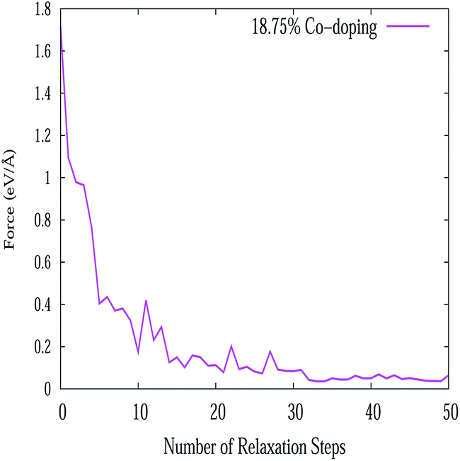
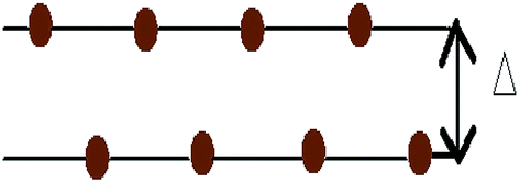
In this work, all the calculations have been performed within the framework of DFT,49–51 using the GGA according to the Perdew–Burke–Ernzerhof (PBE)52 parametrization as implemented in the SIESTA53–55 code. Here we have used the well tested Troullier–Martin56 norm conserving pseudopotentials, in a fully separable form of Kleinman and Bylander for silicon. The double ζ plus polarized basis set is employed through out the whole range of the systems. The Brillouin zone (BZ) has been sampled by using a 20 × 20 × 1 Monkhorst–Pack (MP)57 of k points. A 300 Ry mesh cutoff has been used for the reciprocal space expansion of the total charge density. The diagonalization method is used to perform all the simulations. For constructing the doped system, the Si atoms of the buckled (0.4350 Å) structure are substituted by Al, P and pair of Al–P atoms. In the pristine silicene system three types of substituted atom concentrations have been varied up to 15.62% for AlS and PS systems i.e., 5 dopants in a 32 atom supercell. For the AlPS system, the adatom concentration is varied up to 31.25%, i.e., 5 pairs of dopant atoms in a 32 atom supercell. Throughout the whole calculation we have considered supercells with 32 Si atoms. All these doped structures along with appropriate concentrations are shown in Fig. 1. Structures are optimized by minimizing the forces on individual atoms below 0.02 eV Å−1 using the standard conjugate-gradient (CG) technique. The convergence criteria for the energy of the Self-Consistent Field (SCF) cycle is chosen to be 10−4 eV. The typical force convergence of a given structure with 18.75% co-doping with relaxation time steps is shown in Fig. 2. The specific doping sites for Al, P and Al–P in the silicene network were chosen by considering the configuration with the lowest energy and are consistent with other calculations.58 All the 2D systems were simulated with 15 Å of vacuum in the direction perpendicular to the 2D crystal surface in order to avoid artificial interaction between the artificial images of the 2D sheet. The unit cell of pristine silicene has two Si atoms (A and B) and the space group is P3m1. After the relaxation procedure, the Si–Si, Si–Al and Si–P bond lengths are found to be 2.22, 2.382 and 2.269 Å respectively. It is interesting to note that the geometry of 2D pristine silicene can be visualized as a bipartite lattice consisting of two interpenetrating triangular sublattices of silicon atoms. However, because π bonds between Si atoms are weaker than that of C atoms, the planar structure becomes destabilized,59 and as a consequence, two Si planes are buckled with a height of Δ = 0.4350 Å consistent with the values available in literature (Δ = 0.44–0.45 Å) as shown in Fig. 3.
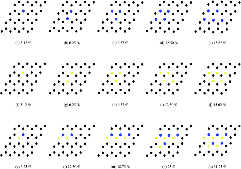 |
| | Fig. 1 Different structures of the doped 32 atom silicene supercells. Black, blue and yellow balls respectively indicate Si, Al and P atoms. (Top) (a)–(e) Different structures of Al doped silicene. (Middle) (f)–(j) Different structures of P doped silicene. (Bottom) (k)–(o) Different structures of Al–P doped silicene. | |
 |
| | Fig. 2 Variation of force convergence with relaxation time steps. | |
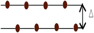 |
| | Fig. 3 Side view of pristine silicene with buckling Δ = 0.4350 Å. | |
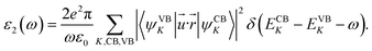
The dielectric properties are calculated by using first-order time dependent perturbation theory. In this procedure dipolar transition matrix elements between occupied and unoccupied single electrons are computed and implemented in the SIESTA code within the formalism of Kohn–Sham (KS).53–55 To calculate the optical properties, sufficient numbers of unoccupied states above the Fermi level have been used. The self-consistent ground state DFT energies and eigenfunctions have been plugged into the dipolar matrix elements to introduce the exchange and correlation effect. In this way the imaginary part of the dielectric function (ε2) has been calculated. The real part (ε1) is calculated with the help of the Kramers–Kronig (KK) transformation.60,61 Optical calculations were done by using a 10 × 10 × 1 optical mesh and 0.2 eV optical broadening. For perpendicular polarization, the direction of the electric field is chosen to be incident perpendicular to the plane of the silicene nanosheet, whereas for parallel polarization, it is chosen to be parallel to the plane of the silicene nanosheet.
The modification of the optical properties with respect to three kinds of impurities have been studied. Optical properties of any system62–64 are in general calculated with the help of a frequency dependent complex dielectric function: ε(ω) = ε1(ω) + iε2(ω). The imaginary part is calculated as mentioned earlier with the help of a time dependent perturbation theory in the simple dipole approximation. In the long wavelength limit (q → 0) the imaginary part of the dielectric function40,53–55,65 is given by,
| |
 | (1) |
In the above expression (1), ω is the frequency of the electromagnetic (EM) radiation in energy units. Ω represents the volume of the supercell and ε0 is the free space permittivity. CB and VB represent the conduction band and the valence band respectively. ![[u with combining right harpoon above (vector)]](https://www.rsc.org/images/entities/i_char_0075_20d1.gif) and
and ![[r with combining right harpoon above (vector)]](https://www.rsc.org/images/entities/i_char_0072_20d1.gif) denote the polarization vector and position vector of the EM field respectively. The real part and the imaginary part of the complex dielectric functions are connected to each other by the KK relation.
denote the polarization vector and position vector of the EM field respectively. The real part and the imaginary part of the complex dielectric functions are connected to each other by the KK relation.
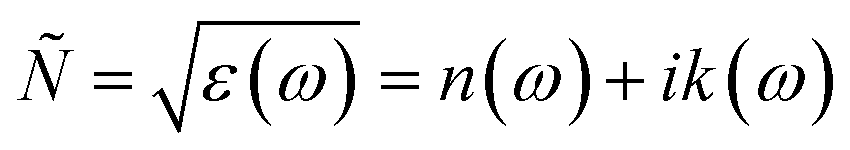
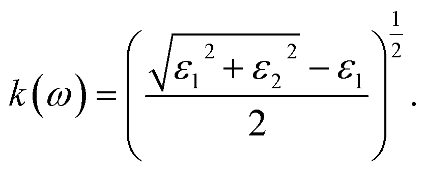
For calculating the optical properties, ε2(ω) data is produced by the SIESTA code. Using this set of data, the complex refractive index (Ñ) of any material can be computed by the relationship 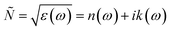 , where,
| |
 | (2) |
| |
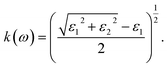 | (3) |
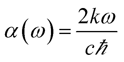
The absorption coefficient can be obtained by using the formula,
| |
 | (4) |
where
c represents the speed of light in vacuum and
ω is in the energy unit.
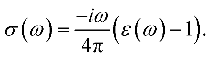
The optical conductivity (σ(ω)) of any material can be calculated by the relation,
| |
 | (5) |
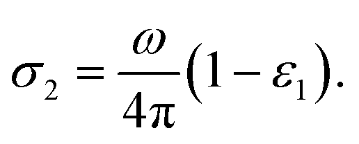
The real and the imaginary part of the optical conductivity is respectively given then by,
| |
 | (6) |
| |
 | (7) |
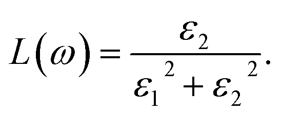
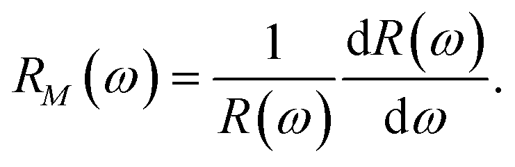
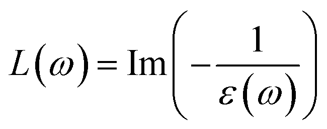
The direct measure of the collective excitation is the quantity called EELS. It is given by the relationship  or in terms of ε1 and ε2,
| |
 | (8) |
The typical energy of the plasmons of a system can be estimated by looking at the peak positions of any loss function. EELS (L(ω)) attain the maximum value when ε1(ω) → 0 and ε2(ω) < 1. All the optical property calculations have been performed in the long wavelength limit q → 0 of the EM wave.
3 Results and discussion
3.1 Formation energy
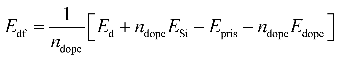
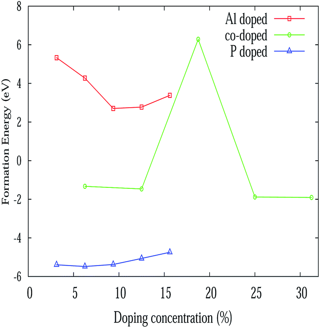
Before studying the optical properties of doped silicene, we studied the defect formation energy of all the structures. The defect formation energy per dopant is defined as
where ndope is the number of dopants, Edf, Ed, ESi, Epris and Edope represent defect formation energy per dopant, total energy of the doped system, energy of a single silicon atom, energy of the pristine silicene system and energy of a single dopant atom respectively. The defect formation energy for Al and P atoms is consistent with the recent binding energy calculation from ab initio calculations for adsorption and absorption in silicene.58 The variation of the defect formation energy per dopant with defect concentration is illustrated in Fig. 4. It is seen from the figure, that P doping is more stable than Al and Al–P doping. Also P doping is exothermic in nature, whereas Al doping is found to be endothermic in nature. The higher stability of the P atoms in contrast can be rooted to the fact that the P–Si bond is slightly shorter while Al–Si bond length is larger by 0.1 Å when compared to the Si–Si bond length.58 This slight increase of Al–Si bond length is due to the lower electronegativity of Al compared to Si. Besides, it has been argued58 that Al substitution reduces the buckling of silicene while P doping restores its buckling character. In fact, P atoms act as acceptors while Al atoms are donors for silicene. For mixed doping, it is observed that the process is exothermic but at an 18.75% co-doping concentration, it suddenly becomes endothermic.
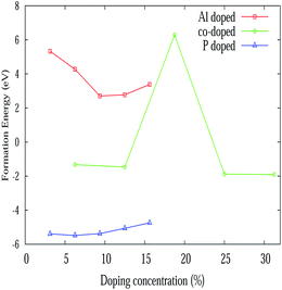 |
| | Fig. 4 Variation of formation energy with various doping concentrations. | |
3.2 Dielectric function
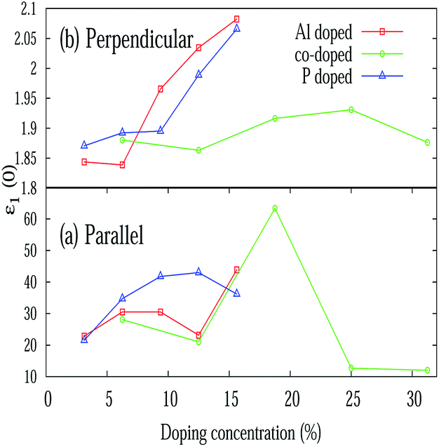
Different optical properties of pristine silicene are depicted in Fig. 5. Fig. 5(a) and (b) respectively depicted the real and imaginary part of the dielectric function of pristine silicene with both parallel (E∥) and perpendicular (E⊥) polarization of the electric field vector of the external EM field in the long wavelength limit (q → 0). The static value of the real part of the dielectric function (ε1(0)) for pristine silicene is respectively given as 5.41 and 1.64 for E∥ and E⊥. The structure peaks in ε2 related to the inter-band transitions, as observed in Fig. 5(b), for parallel (E∥) and perpendicular (E⊥) polarization are situated at 1.01 eV, 3.91 eV, 5.16 eV and 6.18 eV, 8.86 eV respectively. Some of these peaks (3.91 eV and 8.86 eV) are in agreement with the observation in LDA based calculations.47 In addition, the peaks below 3 eV are known47 to be connected with π–π* transitions along the M–K direction while those above 3 eV with σ–σ* transitions along the M–K and Γ–K directions. The variation of ε1(0) with Al, P and Al–P doping is depicted in Fig. 6. In the case of E⊥, for both the AlS and PS systems, we observe an overall increasing tendency, but for the AlPS system, we can see an overall constant behavior. For E∥, in the case of the AlS system, the parabolic shape of the graph is observed. For the PS system, after a slight increase, again it starts decreasing and reaches the minima at 12.50% of doping then again it starts increasing. It would be interesting to see the behavior for even higher P doping concentrations. For the AlPS system of doping, a zigzag behavior is observed with a maximum value at 18.75% co-doping.
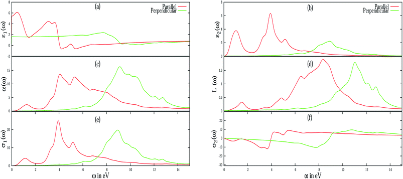 |
| | Fig. 5 Different frequency dependent optical properties of pristine silicene have been illustrated for both E∥ (red line) and E⊥ (green line) of the electric field vector. (a) Real part of ε(ω), (b) imaginary part of ε(ω), (c) absorption coefficient, (d) EELS function, (e) real part of σ(ω), (f) imaginary part of σ(ω). | |
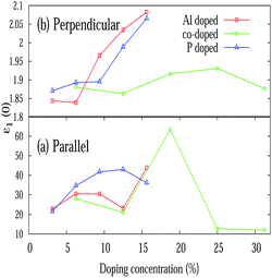 |
| | Fig. 6 Variation of the static value of the real part of the dielectric function (ε1(0)) with various doping concentrations for E∥ and E⊥. | |
3.3 Electron energy loss spectra (EELS)
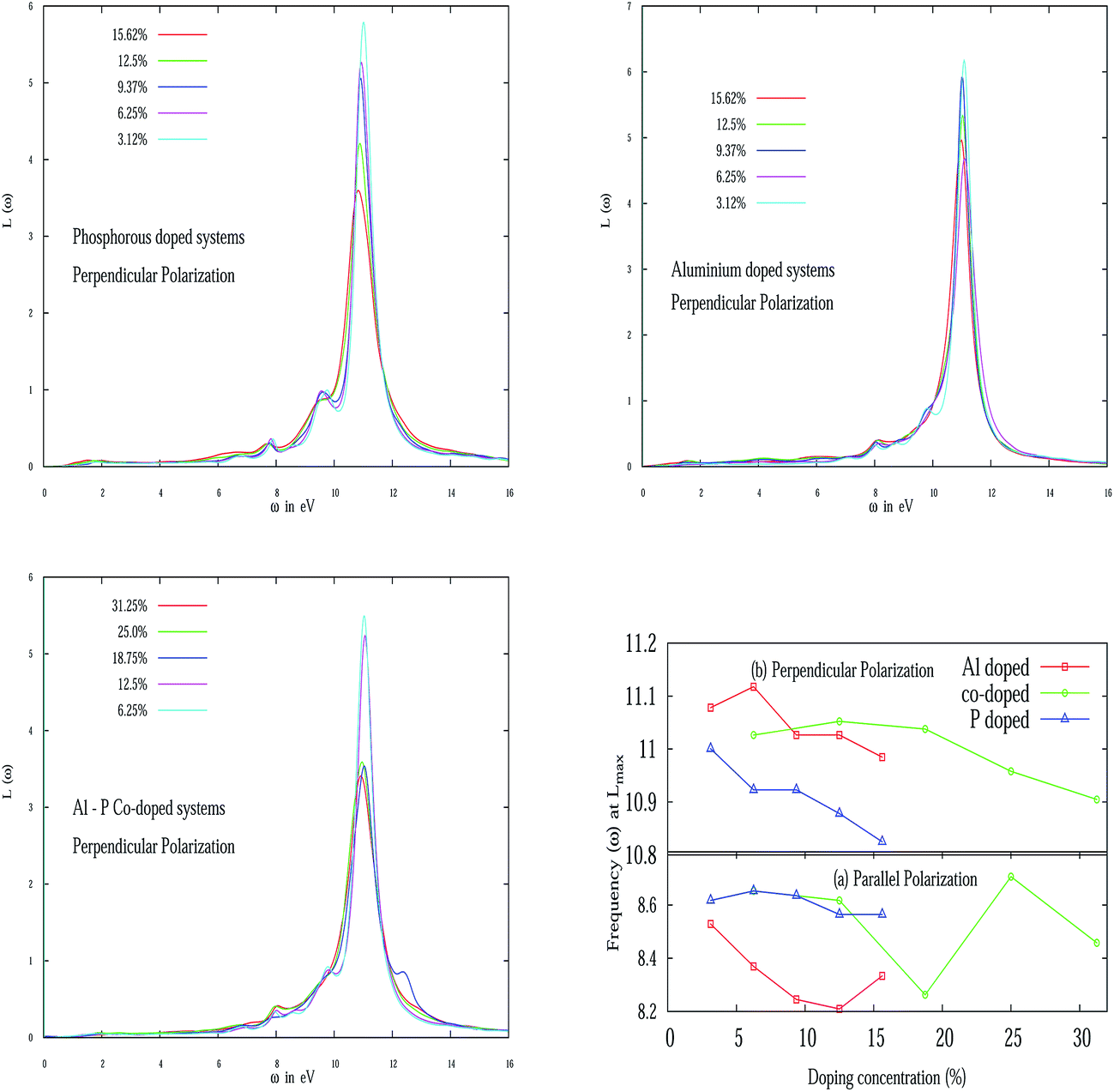
Electron energy loss spectroscopy (EELS) of pristine silicene is depicted in Fig. 5(d). From the figure it is evident that pristine silicene has two plasmon peaks in parallel polarization, one is around 2 eV which is due to the π plasmon and the other is around 9 eV which is due to the π + σ plasmon. In particular, the peak at 2 eV is caused by the transition between π and π* bands around the M and Γ point in the band structure. However, the other peak at 9 eV can be ascribed to the transition between the 4th valence band and the π* conduction band. The peak at 11 eV in perpendicular polarization of pristine silicene can be identified with a third valence band and conduction band in α-silicene. These observations are consistent with the tight-binding calculation of the band structure and the calculation of the dielectric function in the random phase approximation (RPA) for β-silicene45,46 and LDA based calculations.47 For Al and P doped systems, in spite of the presence of some additional peaks in the EELS spectra, it has been observed (not shown in the figure) that the major peaks in parallel polarizations are red-shifted while for perpendicular polarizations, they are blue-shifted when compared to pristine silicene. However, with an increase of doping concentration, all the peaks are red-shifted irrespective of the nature of polarization. The blue-shifting of the peaks in perpendicular polarization is due to the bucking introduced in the silicene nanosheet.
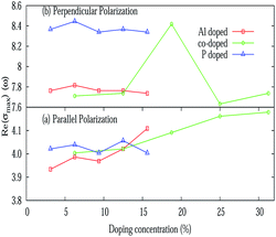
The variation of the EELS peak in perpendicular polarization for various doping concentrations of Al, P and Al–P co-doped systems are presented in Fig. 7. Fig. 7 (top panel left) illustrates the EELS spectra for various P doping concentrations for E⊥. It is to be noted from the figure that two new small peaks appear near 8 eV and 9.5 eV in addition to the large peak around 11 eV. The origin of these two small peaks is possibly due to out of plane plasmon excitation. For parallel polarization, in the Al–P co-doped system, the 2 eV peak in pristine silicene at 6.25% shifted to 2.22 eV. With a further increase in doping concentration, it is shifted to a low energy regime. One of the major peaks around 8 eV is shown in Fig. 7 for various doping concentrations of Al–P. However, for perpendicular polarization apart from the strong peaks around 11 eV and 8 eV, the two small new peaks emerge around 9.78 eV at 6.35% and 12.5%. It is interesting to note that unlike graphene, silicene possesses a small buckling due to Jahn–Teller distortion. Due to this buckling17 it is natural to expect out-of-plane plasmon excitations in silicene and the rich complex structure in EELS as noted recently in the case of pristine silicene.46 We summarize the variation of the maximum EELS peak nature with doping concentration of Al, P and Al–P co-doping in Fig. 7 (bottom panel right). In particular, we schematically plot the frequencies at which EELS attain maximum values with increasing doping concentration. From the figure it is evident that in the case of E⊥ for all three types of doping, an overall decreasing tendency in frequency is observed. But for E∥, for the AlS and PS systems, initially it slightly increases but then again starts decreasing up to 12.50% doping. After that it again starts increasing. Again it would be interesting in the future to see the frequency shift for even higher Al and P doping concentrations. For the AlS and PS systems again a zigzag behavior is observed like the previous case.
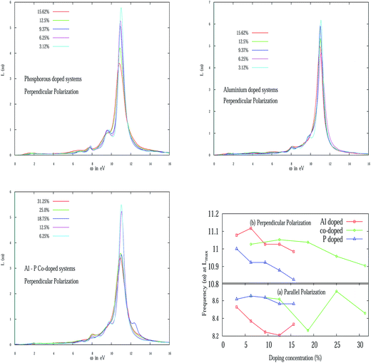 |
| | Fig. 7 (Top panel left) depicts the EELS for some P doped systems for E⊥. (Top panel right) Schematic variation of EELS for the Al doped system. (Bottom panel left) Al–P co-doped system. (Bottom panel right) Variation of frequencies (in eV) of the maximum values of EELS function with various doping concentrations for E∥ and E⊥. | |
3.4 Optical absorption
The absorption coefficient (α(ω)) of pristine silicene is depicted in Fig. 5(c). The maximum value of the absorption coefficient for pristine silicene is 13.55 at an energy of 4.07 eV for E∥ which is within the ultraviolet range and 16.35 at an energy of 9.11 eV for E⊥ which is also in the ultraviolet energy range. For the doped system, the value of the absorption coefficient is higher than the pristine silicene. For parallel polarization, the maximum absorption coefficients are blue-shifted when compared to the pristine system irrespective of doping concentration. While for perpendicular polarization it is interesting to note that for the PS and AlPS systems we observe a red-shift of the maximum absorption coefficients. For the AlS system, depending on the concentration, there is both blue as well as red shift of the maximum value of the absorption coefficients. Fig. 8 illustrates the variation of αmax(ω) with doping concentration. For E⊥, irrespective of the type of doping, all show a decreasing tendency towards high doping concentration. For the PS system, the maximum value of α(ω) is noticed to be within the frequency range of 8–9 eV irrespective of doping concentration. Similarly for the AlS system this value is around 9–10 eV. For AlPS doping this value lies within 9 eV. In the case of E∥, this value is around 4.5 eV, 5 eV and 5–9 eV for the PS, AlS and AlPS systems respectively. Irrespective of doping and polarization, beyond the frequency range of around 15 eV, a very low value of absorption coefficient is observed.
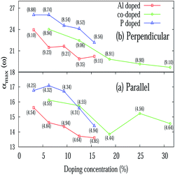 |
| | Fig. 8 Variation of the maximum value of the absorption coefficient (α(ω)) with various doping concentrations for E∥ and E⊥ with frequency measured in eV. | |
3.5 Optical conductivity
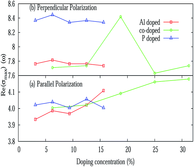
The real (σ1(ω)) and imaginary (σ2(ω)) parts of the frequency dependent optical conductivity of the pristine silicene are depicted in Fig. 5(e) and 3(f) respectively. In the case of pristine silicene the maximum value of the real part is noticed around 4 eV and around 9 eV for E∥ and E⊥ respectively. The maximum value of σ1(ω) for various doping concentrations is illustrated in Fig. 9. For E⊥, more or less constant behavior is observed for both the AlS and PS systems. Whereas for the AlPS system, a sudden jump in the conductivity is observed for an 18.75% doping concentration. For E∥, a characteristic feature is noticed for different types of doping. For the PS system, zigzag behavior is observed, for the AlS system, an increasing tendency is seen and for the AlPS system an overall increasing behavior is observed. So it can be concluded that the optical conductivity of silicene can be controlled by appropriate doping with Al, P or both Al–P. It is worthy to note that the variation of σ1(ω) is consistent with that of the imaginary part of the dielectric function. This naturally serves as a cross-check to our numerical computation. This can shed light for the possible use of silicene in opto-electronic devices.
 |
| | Fig. 9 Variation of the maximum value of the real part of the optical conductivity (σ(ω)) with various doping concentrations for E∥ and E⊥. | |
3.6 Reflectivity modulation
To analyze the spectra of reflectivity, it is desirable to concentrate on the reflectivity (R) modulation with energy (ω) given by,
In fact, reflectivity modulation is a convenient way to analyze the characteristic feature of the reflectivity spectrum of any material.66 It is interesting to note that although R(ω) by its very definition is always positive, RM(ω) can be of any sign. The modulation data for all the doped systems with energy for both type of polarizations are depicted in Fig. 10. The anisotropic features associated with the two polarizations are quite evident from the figure. In particular, for all doped systems, the reflectivity modulation is restricted within low energy (<4 eV) and high energy (>8 eV) for E∥ and E⊥ respectively. For AlS in E∥, the peak below 1 eV with an increase of doping concentration shifts slightly towards a higher energy with varying amplitudes. The same signature continues to exist even for a peak near 2 eV. However, the peak at 8 eV in E⊥ remains robust in its energy position with a small variation of its amplitudes. In E∥ of the PS system, for three different concentrations 3.12%, 6.24% and 9.37% the peak near 2 eV shifts slightly to a higher energy and this peak vanishes with a higher concentration of P. However, the prominent peak near 8 eV in E⊥ sustains its feature till 9.37%. The other significant peak at 10 eV in this system is noticed to change its amplitude very slightly keeping its position fixed with an increase of doping concentration of P. This peak can be identified as one of the characteristic signals of any PS system. For AlPS systems, the existence of two significant peaks at 8 and 10 eV in E⊥ is important for all concentrations. The presence of multiple peaks in E⊥ at high energy and E∥ at low energy is again an indication of buckling in the silicene system.
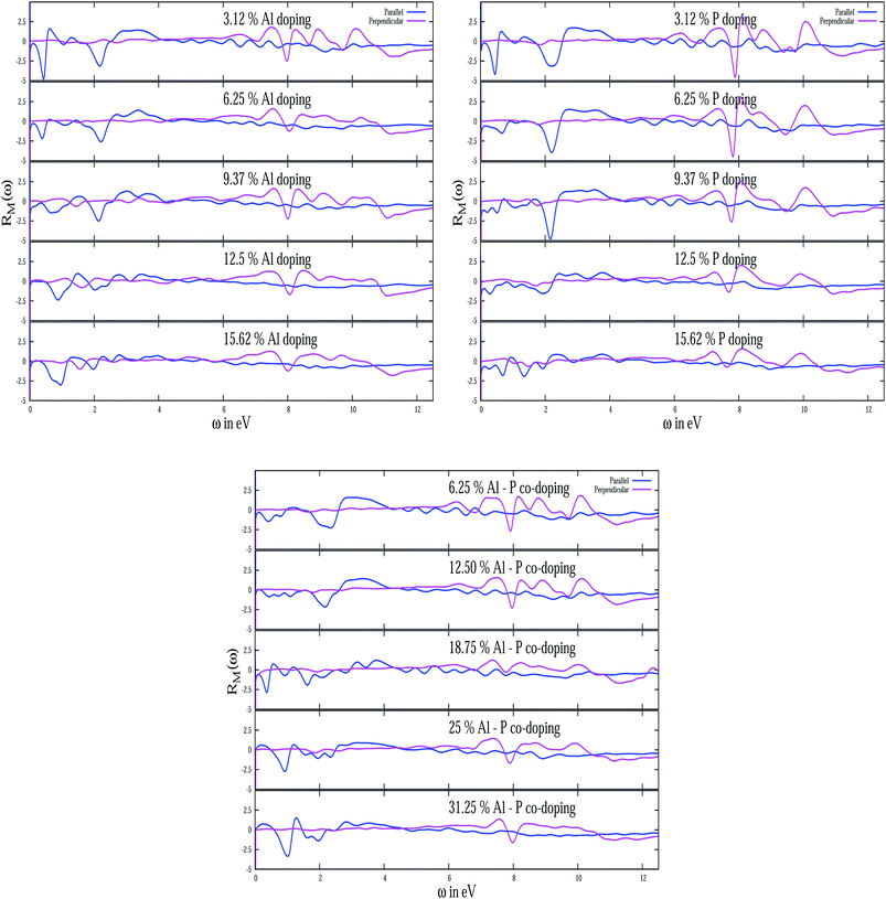 |
| | Fig. 10 The reflectivity modulation with energy for various doping concentrations of Al, P and Al–P co-doped for both type of polarizations. | |
4 Conclusions
In summary, the optical properties of free standing silicene with various concentrations of Al, P and Al–P co-doping have been performed in the framework of DFT in the long wavelength limit. It is demonstrated from the formation energy that structures with P doping are more stable compared with other doped ones. With an increase of doping concentration, the peaks in EELS spectra are red-shifted irrespective of the nature of polarization. At particular P doping concentrations, a new additional significant EELS peak is observed in perpendicular polarization. It is also noted that for doped systems the value of the absorption coefficient is higher than the pristine silicene and is restricted within the ultraviolet range. Although no significant changes are indicated at the maximum values of optical conductivity with doping concentration in perpendicular polarization, however, a sudden jump appears for the Al–P codoped system at 18.75% doping concentration. For all doped systems, the reflectivity modulation is restricted within low energy (<4 eV) and high energy (>8 eV) for E∥ and E⊥ respectively. The presence of multiple peaks in the modulation can be related to the buckling of the silicene. Although the above theoretical results are obtained with GGA and 32 atoms, we believe that these predicted results may give a strong indication to expected results in an experimental situation with Al and P doped silicene systems. All these theoretical observations are expected to shed light on fabricating opto-electronics devices using silicene as the block material.
Acknowledgements
This work is partially supported by DST-FIST, DST-PURSE, Government of India. Two of the authors (RD and SC) gratefully acknowledge DST, Government of India for providing financial assistance through the DST-INSPIRE Fellowship scheme. The authors would also like to take this opportunity to thank two anonymous reviewers for their critical comments and suggestions.
References
- A. K. Geim and I. V. Grigoriera, Nature, 2013, 499, 419 CrossRef CAS PubMed.
- M. Xu, T. Liang, M. Shi and H. Chen, Chem. Rev., 2013, 113, 3766 CrossRef CAS PubMed.
- V. Nicolosi and M. Chhowala, et al., Science, 2013, 340, 1226419 CrossRef.
- R. M. Balleste and C. G. Navarro, et al., Nanoscale, 2011, 3, 20 RSC.
- L. C. L. Y. Voon and G. G. G. Veri, MRS Bull., 2014, 39, 366 CrossRef CAS . See also: G. G. G. Veri and L. C. L. Y. Voon, Phys. Rev. B: Condens. Matter Mater. Phys., 2007, 76, 75131 CrossRef.
- N. D. Mermin, Phys. Rev., 1968, 176, 250 CrossRef.
- H. O’Hare, F. V. Kusumartsov and K. I. Kugel, Nano Lett., 2012, 12, 1045 CrossRef PubMed.
- N. J. Roome and J. D. Caret, ACS Appl. Mater. Interfaces, 2014, 6, 7743 CAS.
- E. Scalise, M. Houssa and G. Pourtois, et al., Nano Res., 2013, 6, 19 CrossRef CAS.
- D. Jose, A. Nijamudheen and A. Datta, Phys. Chem. Chem. Phys., 2013, 15, 8700 RSC.
- W.-F. Tsai, C.-Y. Huang, T.-R. Chang, H. Lin, H.-T. Jeng and A. Bansil, Nat. Commun., 2013, 4, 1500 CrossRef PubMed.
- H. Behera and G. Mukhopadhyay, A Comparative computational study of the electronic properties of planar and buckled silicene, arXiv:1201.1164.
- A. Kara, et al., J. Supercond. Novel Magn., 2009, 22, 259 CrossRef CAS.
- B. Aufray, et al., Appl. Phys. Lett., 2010, 96, 183102 CrossRef PubMed.
- D. E. Padova and C. Quaresima, et al., Appl. Phys. Lett., 2011, 98, 081909 CrossRef PubMed.
- H. Nakano and T. Mitsuoka, et al., Angew. Chem., 2006, 118, 6451 CrossRef.
- S. Lebgue and O. Eriksson, Phys. Rev. B: Condens. Matter Mater. Phys., 2009, 79, 115409 CrossRef.
- H. Sahin, S. Cahangirov, M. Topsakal, E. Bekaroglu, E. Aktrk, R. T. Senger and S. Ciraci, Phys. Rev. B: Condens. Matter Mater. Phys., 2009, 80, 155453 CrossRef.
- S. Cahangirov, M. Topsakal, E. Aktrk, H. Sahin and S. Ciraci, Phys. Rev. Lett., 2009, 102, 236804 CrossRef CAS.
- S. Wang, J. Phys. Soc. Jpn., 2010, 79, 064602 CrossRef.
- M. Houssa, G. Pourtois, V. V. Afanasev and A. Stesmans, Appl. Phys. Lett., 2010, 97, 112106 CrossRef PubMed.
- B. Lalmi, H. Oughaddou, H. Enriquez, A. Kara, S. Vizzini, B. Ealet and B. Aufray, Appl. Phys. Lett., 2010, 97, 223109 CrossRef PubMed.
- P. Vogt, P. D. Padova, C. Quaresima, J. Avila, E. Frantzeskakis, M. C. Asensio, A. Resta, B. Ealet and G. L. Lay, Phys. Rev. Lett., 2012, 108, 155501 CrossRef.
- N. Y. Dzade, K. O. Obodo, S. K. Adjokatse, A. C. Ashu, E. Amankwah, C. D. Atiso, A. A. Bello, E. Igumbor, S. B. Nzabarinda, J. T. Obodo, A. O. Ogbuu, O. E. Femi, J. O. Udeigwe and U. V. Waghmare, J. Phys.: Condens. Matter, 2010, 22, 375502 CrossRef PubMed.
- D. Jose and A. Datta, Phys. Chem. Chem. Phys., 2011, 13, 7304 RSC.
- M. J. S. Spencer, T. Morishita, M. Mikami, I. K. Snook, Y. Sugiyama and H. Nakano, Phys. Chem. Chem. Phys., 2011, 13, 15418 RSC.
- T. H. Osborn, A. A. Farajian, O. V. Pupysheva, R. S. Aga and L. C. L. Y. Voon, Chem. Phys. Lett., 2011, 511, 101 CrossRef CAS PubMed.
- P. D. Padova, C. Quaresima, C. Ottaviani, P. M. Sheverdyaeva, P. Moras, C. Carbone, D. Topwal, B. Olivieri, A. Kara, H. Oughaddou, B. Aufray and G. L. Lay, Appl. Phys. Lett., 2010, 96, 261905 CrossRef PubMed.
- A. Kara, H. Lneiquez and A. P. Seitsonen, et al., Surf. Sci. Rep., 2012, 67, 1 CrossRef CAS PubMed.
- E. Cinquanta, E. Scalise and D. Chiappe, et al., J. Phys. Chem. C, 2013, 117, 16719 CAS.
- C. Kamal, http://arxiv.org/abs/1202.2636. See also: C. Kamal, A. Chakrabarti, A. Banerjee and S. K. Deb, J. Phys.: Condens. Matter, 2013, 25, 085508 CrossRef CAS PubMed.
- Z. Ni, Q. Liu, K. Tang, J. Zheng, J. Zhou, R. Qin, Z. Gao, D. Yu and J. Lu, Nano Lett., 2012, 12, 113 CrossRef CAS PubMed.
- N. D. Drummond, V. Z. Lyomi and V. I. Falko, Phys. Rev. B: Condens. Matter Mater. Phys., 2012, 85, 075423 CrossRef.
- M. Ezawa, New J. Phys., 2012, 14, 033003 CrossRef.
- D. Jose and A. Datta, J. Phys. Chem. C, 2012, 116, 24639 CAS.
- D. Jose and A. Datta, Acc. Chem. Res., 2014, 47, 593 CrossRef CAS PubMed.
- P. Nath, D. Sanyal and D. Jana, Physica E, 2014, 56, 64 CrossRef CAS PubMed.
- P. Rani and V. K. Jindal, RSC Adv., 2013, 3, 802 RSC.
- P. Rani and V. K. Jindal, Stability and electronic properties of isomers of B/N co-doped graphene, Appl. Nanosci., 2013, 4, 989, DOI:10.1007/s13204-013-0280-3.
- P. Nath, S. Chowdhury, D. Sanyal and D. Jana, Carbon, 2014, 73, 275 CrossRef CAS PubMed.
- D. Jana, P. Nath and D. Sanyal, Modifications of Electronic properties of Graphene by Boron (B) and Nitrogen (N) substitution, To appear as a chapter in CRC Press/Taylor & Francis, 2014 Search PubMed.
- V. O. Özcelik and S. Ciraci, Phys. Rev. B: Condens. Matter Mater. Phys., 2012, 86, 155421 CrossRef.
- A. Majumdar, S. Chowdhury, P. Nath and D. Jana, RSC Adv., 2014, 4, 32221 RSC.
- L. Rast, and V. K. Tewary, Electron Energy Loss Function of Silicene and Germanene Multilayers on Silver, 2013, arxiv: 1311:0838v1.
- K. Chinnathambi, A. Chakrabarti, A. Banerjee and S. K. Deb, Optical Properties of Graphene-like Two Dimensional Silicene, 2012, arXiv:1205.5099 [cond-mat.mes-hall].
- L. M. Priede and L. Meza-Montes, Electron-Energy-Loss Spectra of Free-Standing Silicene, 2014, arXiv:1405.4205 [cond-mat.mes-hall].
- B. Mohan, A. Kumar and P. K. Ahluwalia, Physica E, 2013, 53, 233 CrossRef CAS PubMed.
- L. Matthes, O. Pulici and F. Bechstedt, J. Phys.: Condens. Matter, 2013, 25, 395305 CrossRef PubMed.
- P. Hohenberg and W. Kohn, Phys. Rev., 1964, 136B864 Search PubMed.
- W. Kohn and L. J. Sham, Phys. Rev., 1965, 140, A1133 CrossRef.
- W. Kohn, Rev. Mod. Phys., 1999, 71, 1253 CrossRef CAS.
- J. P. Perdew, K. Burke and M. Ernzerhof, Phys. Rev. Lett., 1996, 77, 3865 CrossRef CAS.
- P. Ordejon, E. Artacho and J. M. Soler, Phys. Rev. B: Condens. Matter Mater. Phys., 1996, 53, R10441 CrossRef CAS.
- D. Sanchez-Portal, P. Ordejon, E. Artacho and J. M. Soler, Int. J. Quantum Chem., 1997, 65, 453 CrossRef.
- J. M. Soler, E. Artacho, J. D. Gale, A. Garca, J. Junquera, P. Ordejon and D. Sanchez-Portal, J. Phys.: Condens. Matter., 2002, 14, 2745 CrossRef CAS ; see also http://www.uam.es/siesta.
- N. Troullier and J. L. Martins, Phys. Rev. B: Condens. Matter Mater. Phys., 1991, 43, 1993 CrossRef CAS.
- H. J. Monkhorst and J. D. Pack, Phys. Rev. B: Condens. Matter Mater. Phys., 1976, 13, 5188 CrossRef.
- J. Sivek and H. Sahin, et al., Phys. Rev. B: Condens. Matter Mater. Phys., 2013, 87, 085444 CrossRef.
- H.-X. Luan, C.-W. Zhang, F.-B. Zheng and P. Wang, J. Phys. Chem. C, 2013, 117, 13620 CAS.
- G. D. Mahan, Many Particle Physics, New York, Plenum Press, 1990 Search PubMed.
- M. Dressel and G. Gruner, Electrodynamics of Solids, Cambridge University Press, Cambridge, 2002 Search PubMed.
- D. Jana, L.-C. Chen, C. W. Chen, S. Chattopadhyay and K. H. Chen, Carbon, 2007, 45, 1482 CrossRef CAS PubMed.
- D. Jana, A. Chakraborty, L.-C. Chen, C. W. Chen and K. H. Chen, Nanotechnology, 2009, 20, 175701 CrossRef PubMed.
- S. Chowdhury, R. Das, P. Nath, D. Sanyal and D. Jana, Electronic and Optical properties of Boron and Nitrogen functionalized graphene nanosheet, accepted by CRC Publications, Taylor & Francis, 2014 Search PubMed.
- D. Jana, C. L. Sun, L.-C. Chen and C. H. Chen, Prog. Mater. Sci., 2013, 58, 565 CrossRef CAS PubMed.
- P. Y. Yu and M. Cardona, Fundamentals of Semiconductors Physics and Materials Properties, Springer Publication, 4th edn, 2010, ch. 6 Search PubMed.
Footnote |
| † Present address: University of Saskatchewan, Saskatoon, Canada S7N 5A1. |
|
| This journal is © The Royal Society of Chemistry 2015 |
Click here to see how this site uses Cookies. View our privacy policy here. 


 , where,
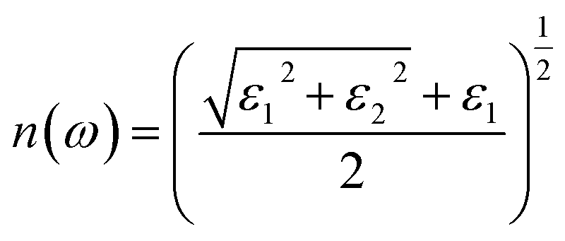

 or in terms of ε1 and ε2,