
Photoinduced synthesis of Ag nanoparticles on ZnO nanowires for real-time SERS systems
Hyun Wook Kangab,
Juyoung Leema and
Hyung Jin Sung*a
aDepartment of Mechanical Engineering, KAIST, 291 Daehak-ro, Yuseong-Gu, Daejeon 305-701, Korea. E-mail: hjsung@kaist.ac.kr
bDepartment of Mechanical Engineering, Chonnam National University, 77 Yongbong-ro, Buk-gu, Gwangju 500-757, Korea
First published on 1st December 2014
Abstract
We developed a photoinduced synthesis method for fabricating metal nanoparticles (NPs) embedded on the surfaces of metal oxide nanowires (NWs) to form hierarchical nanostructures. The process consisted of two steps: (1) the preparation of a metal oxide NW backbone structure, and (2) the photoinduced synthesis of metal NPs on the backbone structure. ZnO NWs were first prepared and reduced to form metal oxide NWs. UV light was used to generate electron–hole pairs at the metal oxide NW surface. The excited electrons successfully reduced Ag ions in solution to form Ag NPs on the ZnO NW surfaces without introducing contamination or side-reactions. The surface-enhanced Raman spectroscopy (SERS) properties of the hierarchical materials were investigated for various Ag nanostructure morphologies. The SERS activity revealed an outstanding enhancement factor of 6.36 × 10¹¹. A range of glucose solution concentrations was detected using the SERS method in conjunction with the hierarchical materials. The hierarchical materials were deployed in a microfluidic system to sequentially detect distinct molecules as they flowed through the channel. The photoinduced synthesis process required only simple, low-cost, and environmentally benign fabrication conditions.
1 Introduction
The identification of specific molecules or trace indicators is essential for many application areas in medicine, pharmacology, genetics, analytical chemistry, and biology.1–5 The detection of concentration variations in a chemical or biomaterial is required in certain contexts as an extension of the analytical capabilities.6–10 The detection of low concentrations or small quantities of an analyte requires highly sensitive detection techniques for reproducibility and accuracy. Raman spectroscopy provides fingerprint spectra, even under extremely low analyte concentration conditions, without the need for labeling steps.11 Despite its advantages, the intensity of a Raman spectrum is typically too small to be applied as a sensing technique; therefore, surface-enhanced Raman spectroscopy (SERS) techniques were developed using the active materials in an effective arrangement.12–14Continuous SERS detection techniques is achieved when SERS method is integrated with microfluidic systems, which offer rapid, sensitive, in situ real-time sensing.15–20 For microfluidic SERS device, metals such as gold (Au), silver (Ag), or copper (Cu) are prepared in microstructured film which is called SERS-active substrate.21–24 Among these materials, Ag nanostructures have provided the best SERS activity due to its optical and electronic properties which results from localized surface plasmon resonance (LSPR) effects.25,26 LSPR effects are governed by the shape of the metal nanostructures and the gap distance between the adjacent nanostructures. Typically, ∼1 nanometer gaps between 100 nanometer metal structures provide the best resonance conditions.27–29 Most SERS-active substrates have been fabricated using metal thin film deposition techniques, such as physical vapor deposition30,31 of thermal and electron beam evaporation32,33 with post-thermal treatment to generate a nanostructure. Despite the advantages of well-defined and easy fabrication processes, these methods have required high-vacuum and high temperature conditions, and have provided limited SERS efficiencies due to the restriction of plasmon resonances within a two-dimensional plane.
Recently, three-dimensional hierarchical structures have been examined for additional Raman enhancement. Metal NPs were deposited onto anisotropic micro- or nano-structures to increase the number of NPs per unit area. Ag NPs were used to decorate glass nanopillar arrays, which enhanced the SERS sensing signal by a factor of 10 relative to the enhancement achieved using Ag NPs on a planar surface. The controllable anisotropic structure of the glass nanopillars generated a high detection volume and more hot spots that could enhance the Raman signal.34 Metal (Au and Ag) NP-coated single wall carbon nanotubes (SWCNTs) were developed as a SERS-active material to investigate DNA and study cells.35 Silver-metallized reactive ion-etched silicon nanopillars have provided a high SERS enhancement factor on the order of 1011.28 These fabrication methods tend to require complex pretreatment processes, such as physical or chemical etching, and they are limited to select materials that can present obstacles to integration with useful systems, such as microfluidic channels.
This study describes a fabrication strategy for preparing metal NPs embedded onto metal oxide nanowires (NWs) integrated into a microfluidic system for continuous SERS detection. Patterned ZnO NWs were prepared as a backbone structure using low-temperature hydrothermal synthetic processes.36,37 After the ZnO NWs had been prepared, AgNO3 was dissolved in deionized (DI) water to form a Ag precursor. ZnO NWs were immersed in the Ag precursor and exposed to ultraviolet (UV) to induce the formation of Ag NPs on the ZnO NW surfaces.38 The UV exposure energy could be controlled to tune the Ag nanostructure morphology, and the resulting SERS enhancement was examined. Finally, the Ag NPs embedded on the ZnO NWs were integrated into a microfluidic channel to provide a real-time SERS platform for efficient continuous biomolecule sensing.
2 Results and discussion
2.1 Photoinduced synthesis of Ag NPs embedded onto ZnO NW surfaces
The photoinduced synthesis of NPs embedded onto the surfaces of NWs, forming a hierarchical structure, was conducted using electrons to reduce metal ions to the metal. Semiconductor metal oxide materials with an appropriate band gap, here, ZnO NWs, were used as the electron provider. UV irradiation of the semiconductor materials generated an electron–hole pair by exciting the peripheral electrons. Inside the metal ion solution, the electrons generated at the semiconductor material surface encountered the metal ions and reduced them to a metal. In addition to providing an electron source under irradiation, the ZnO NWs also provided a backbone structure onto which the silver ions were reduced to silver NPs. The photoinduced synthesis of metal NPs embedded on the surfaces of metal oxide NWs consisted of two steps: (1) preparation of a metal oxide NW backbone structure, and (2) UV exposure for the synthesis of metal NPs on the backbone structure. A schematic illustration of the photoinduced synthesis process is shown in Fig. 1a–c.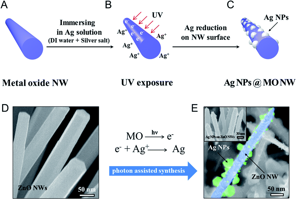 | ||
| Fig. 1 Schematic diagram illustrating the photoinduced synthesis process for preparing nanoparticles (NPs) on metal oxide nanowires (NWs). (A) The NWs were prepared, and (B) immersed into a silver ion solution (deionized water + silver salt (AgNO3)). As a result, (C) a hierarchical structure consisting of Ag NPs embedded on the NW surfaces was achieved. The corresponding SEM images of (D) the ZnO NWs and (E) the Ag NPs embedded on the ZnO NW surfaces. | ||
Vertically aligned ZnO NWs were synthesized using hydrothermal methods to form the metal oxide NW backbone material. The Ag NPs embedded on the ZnO NW surfaces were prepared using a 0.1 M AgNO3 aqueous solution (Ag precursor). The ZnO NW substrate was then immersed into the Ag precursor and exposed to UV. During the UV exposure process, photons induced electron excitation on the oxide NW surface. The excited electrons met the Ag ions in the solution and reduced the Ag ion to Ag NPs at the ZnO NW surfaces. The wavelength of UV was 312 nm and the power was 15 mW (UV source from Midas System, MDS-60MS). Based on Planck's equation, required wavelength for electron generation in ZnO NWs must be less than 368 nm (in the UV region). The UV irradiation (λ ∼ 312 nm) generated electrons in the ZnO NWs that reduced the Ag ions to form Ag,
 | (1) |
During the synthesis, Ag NPs are generated only on ZnO NW surfaces because UV stimulates electron generation inside of ZnO NWs. Microchannel fabrication for the application became easier due to this generation of Ag NPs in selective regions. Fig. 1d and e show scanning electron microscopy (SEM) images of, respectively, bare ZnO NWs and the successful embedding of Ag NPs on ZnO NW surfaces.
The surface morphologies were analyzed quantitatively using transmitted electron microscopy (TEM), energy-dispersive X-ray spectroscopy (EDX), and X-ray diffraction (XRD) studies. Fig. 2a shows a TEM image of Ag NPs embedded on ZnO NWs. Ag NPs 2–10 nm in diameter were homogeneously synthesized on ZnO NWs. The high-resolution transmitted electron microscopy (HRTEM) image shown in Fig. 2b revealed a high-quality crystalline structure of the interface region between the ZnO NW surfaces and the Ag NPs, and the ZnO NW structure remained intact. The NPs grew on the [001] face of the ZnO NWs, with lattice spacing of 0.52 nm, and on the [111] face, with lattice spacing of 0.23 nm.
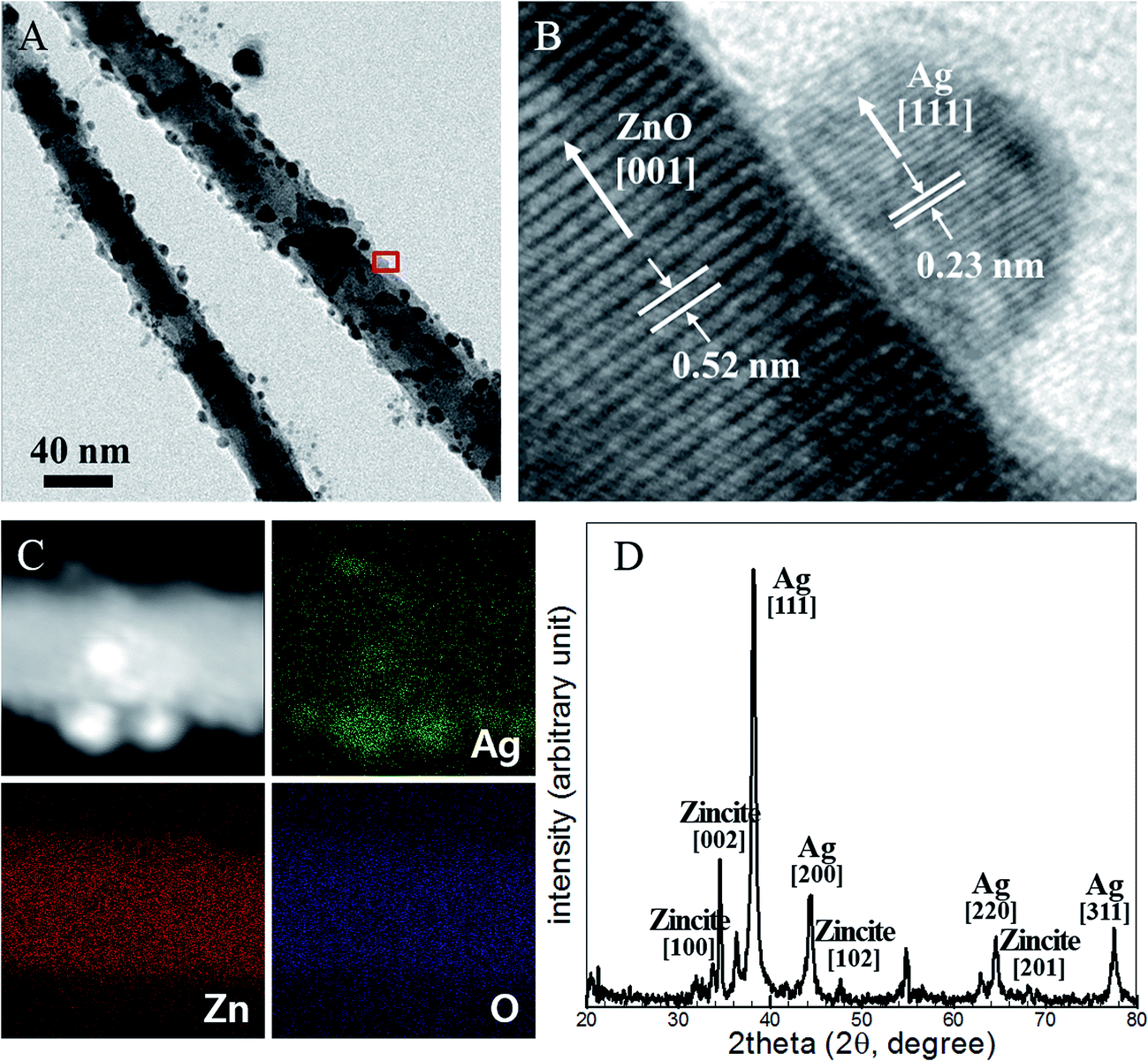 | ||
| Fig. 2 (A) TEM and (B) HRTEM images of the Ag NPs embedded on the ZnO NW surfaces. (C) High-angle annular dark field scanning transmission electron microscopy (HAADF-STEM) image of the Ag NP-embedded hierarchical structure-embedded ZnO NW surface, and the corresponding TEM-EDS elemental maps of Ag, Zn, and O. (D) XRD patterns collected from the Ag NPs and ZnO NW hierarchical structures. | ||
Fig. 2c shows high-angle annular dark field scanning transmission electron microscopy (HAADF-STEM) and EDX images that demonstrate the high purity of the Ag NPs following their photoinduced synthesis. The EDX maps of elemental silver (Ag), zinc (Zn), and oxide (O) revealed that diffusion into or chemical reactions with the Ag NPs did not occur during the synthetic process. The XRD analysis indicated that the synthesized NPs were composed predominantly of Zn and Ag, as shown in Fig. 2d. The higher XRD intensity of the Ag signal compared to the Zn signal was due to the high surface distribution of Ag NPs, which attenuated the X-ray illumination prior to entry into the ZnO NWs and reflected the signal. The Ag NPs were successfully generated at the ZnO NW surfaces and they form ZnO NW/Ag NP hierarchical structure. The single crystalline Ag NPs were attached directly on the ZnO NW surfaces without the need for additional components and without introducing damage. The process described here is easily performed and requires a light source, room-temperature conditions, and ambient pressure conditions. These advantages enable this process to be utilized for flexible substrate-based electronic and photonic devices. The process can reduce production costs by permitting roll-to-roll mass production.
2.2 Geometry control over the Ag NPs
Controlling the size and morphology of the Ag NPs was essential because Raman enhancement depends on the particle size as well as gap distance between adjacent particles. Various Ag NP geometries were achieved using the photoinduced synthesis method by controlling the total amount of UV exposure energy during the synthetic process. Fig. 3 shows the various Ag NP geometries, depending on the UV exposure energy, adjacent to the corresponding SEM analysis. Ag NPs prepared via exposure to 5 J UV irradiation were characterized by 10–20 nm diameters, and the Ag NP surface coverage density was around 50%. As the UV exposure energy increased, both the average diameter of the Ag NPs and the surface coverage density increased. An increase in the Ag NP size did not change over the energy range of 5–20 J, although the average diameter increased slightly from 15 to 20 nm. On the other hand, the surface coverage density increased dramatically from 50 to 100%. At this coverage density, the average gap distance increased the SERS performance. UV exposure energies exceeding 25 J yielded a surface coverage density of 100%. The surface morphology, however, changed as the thin film formed, and the Ag NPs did not maintain their particulate morphology. The surface roughness decreased as the exposure energy increased, as shown in Fig. 3e and f, because Ag reduction proceeded as the thin film formed.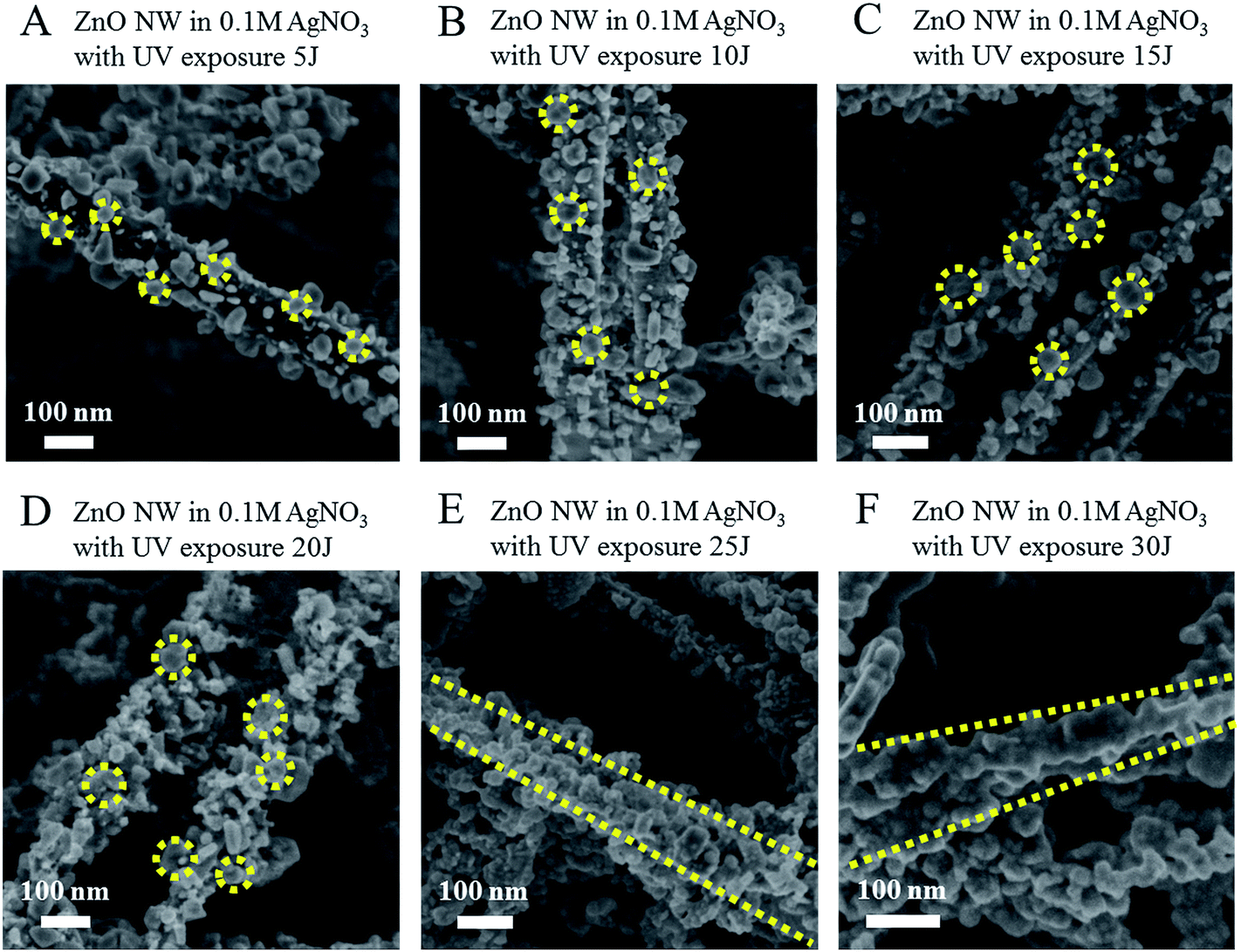 | ||
| Fig. 3 SEM images of the Ag NPs embedded on the ZnO NW surfaces prepared by immersing ZnO NWs in a 0.1 M AgNO3 DI solution, with UV irradiation energies of (A) 5 J, (B) 10 J, (C) 15 J, (D) 20 J, (E) 25 J, and (F) 30 J. | ||
2.3 Measurements of the SERS properties
The Raman signal intensities of the Ag NPs fabricated on the ZnO NWs were measured as a function of the total UV exposure energy. The results are shown in Fig. 4. The Raman signal intensity increased as the UV exposure energy increased over the range 5–20 J. On the other hand, the Raman signal intensity decreased to a greater extent when the UV exposure energy exceeded 25 J. This effect resulted from changes in the Ag NP structural geometry. When UV exposure energies of less than 20 J were applied, the generated Ag nanoparticles have diameters of 10 nm. The gap distance between Ag NPs decreased as the UV exposure energy increased. UV exposure energies exceeding 25 J, however, provided a poor Raman signal intensity because the Ag structures formed a thin film without any gaps between adjacent Ag NPs. Metal thin films are not effective for increasing the Raman signal intensity due to low LSPR effects. The distance between ZnO NW backbone structures is an important parameter for SERS applications. Backbone structure dimensions smaller than those of the synthesized metal NPs cannot provide good SERS-active materials. In this study, the average backbone structural dimensions of the ZnO NWs were 30 nm. The hierarchical structures produced by 20 J UV irradiation yielded individual Ag NPs on the ZnO NW surface and provided an excellent SERS-based molecular detection system.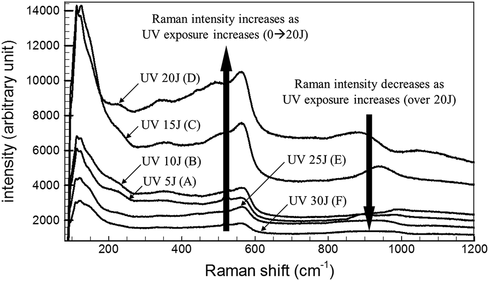 | ||
| Fig. 4 Raman spectra of the Ag NPs embedded on the ZnO NW surfaces as a function of the UV exposure energy. The Raman signal intensity increased as the UV exposure increased (0–20 J), and decreased as the UV exposure increased (beyond 20 J). | ||
2.4 Microfluidic system for real-time SERS detection
The photoinduced synthesis of the Ag NPs on the ZnO NW surfaces is advantageous for integrating the patterned hierarchical ZnO NW array structures into a microfluidic system. Patterned ZnO NWs were prepared using microcontact printing techniques.36,37 Patterned ZnO NWs were prepared through a two-step process. First, a ZnO NP seed material used for hydrothermal synthesis was patterned onto the silicon wafer substrate. Second, the seed material-patterned substrate was immersed into an aqueous solution containing zinc ions and polymer encapsulators and it was heated for 6 hours at 95 °C. The patterned region was rectangular, 3 mm × 15 mm. The 3 mm width was sufficient to enable detection of the SERS signal because SERS detection regions are typically less than 30 μm in diameter. A microfluidic channel was fabricated using polydimethylsiloxane (PDMS) and had a 30 μm in height, a 5 mm in width, and an 18 mm in length. The ZnO NW patterning method and Ag NP photoinduced synthesis process were used to embed Ag NPs onto the surfaces of a ZnO NW array only within the ZnO NW patterned region. A schematic illustration of the fabrication process used to pattern the Ag NPs embedded on the ZnO NW surfaces within a microfluidic channel is shown in Fig. 5. The patterned ZnO NWs with Ag NP structures on a silicon substrate were fabricated using an open microfluidic channel and a cover glass by applying oxygen plasma bonding techniques. Although the PDMS channel was clear and transparent enough to use as a laser window, a cover glass was introduced as an illumination and observation window to avoid the detection of weak or distorted SERS signals.18 After fabrication, a detectable target analyte was injected into the microfluidic channel, and the SERS signal was measured using a laser control module and a Raman signal detector. | ||
| Fig. 5 Schematic illustration of the process used to fabricate patterned Ag NP-embedded ZnO NWs within a microfluidic channel, and the in situ, real-time SERS signal detection device. | ||
Glucose (C6H12O6) was used as the detection analyte due to its importance in biological and medical research and treatment. Glucose was dissolved in DI water in various concentrations (1 mM, 1 μM, 1 nM, 1 pM, and 1 fM), and the solution concentrations were measured according to the Raman signal intensity using the fabricated SERS device. Fig. 6a shows the Raman signal intensities as a function of the glucose concentration. The Raman signal intensity increased as the glucose concentration increased. This differences in the signal intensities suggested that the analyte concentration changes could be detected over time using the microfluidic SERS detection system. The solution concentration was varied, as shown in Fig. 6b. Each concentration was injected over 1 min under a 100 μL min−1 flow rate. The concentration of the injected solution was lowered stepwise and then increased: 1 mM, 1 nM, 1 fM, 1 nM, and 1 mM. The Raman signal intensity of each analyte solution was measured in 20 s time intervals. The measured real-time glucose concentration changes are shown in Fig. 6c (red signal: 1 mM; green signal: 1 nM; black signal: 1 fM). As the concentration was reduced (increased), the SERS signal intensity immediately decreased (increased), indicating that the Ag NPs embedded on the ZnO NW surfaces in the microfluidic channel permitted the in situ continuous SERS detection during injection.
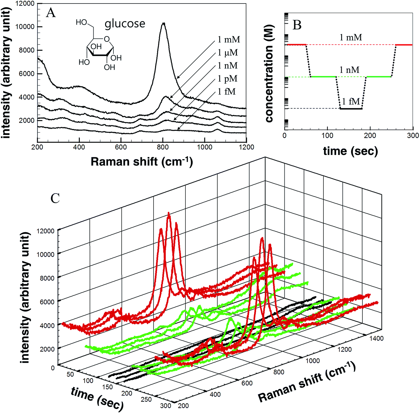 | ||
| Fig. 6 (A) Raman spectra of Ag NP-embedded ZnO NWs, prepared with an exposure power of 20 J, at various analyte (glucose) concentrations of 1 mM, 1 μM, 1 nM, 1 pM, and 1 fM. (B) The concentrations of the glucose solutions flowed through the channels at a rate of 100 μL min−1. (C) Measured real-time SERS signal as a function of the analyte concentrations over time. The color of lines indicate glucose concentration; (black: 1 fM, green: 1 nM, red: 1 mM). | ||
A more quantitative analysis was undertaken by measuring the analyte SERS signal intensity (mmc) and calculating the concentration according to
 | (2) |
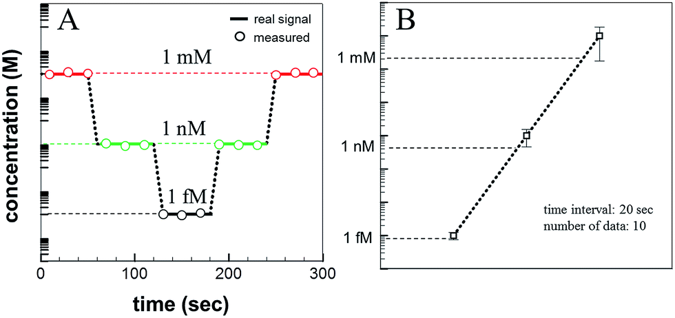 | ||
| Fig. 7 (A) Sequentially calculated glucose concentrations, determined using the microfluidic SERS system, over time. (B) Error analysis of the microfluidic SERS system. | ||
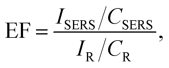
2.5 SERS enhancement factor
Practical applications require the calculation of the SERS enhancement factor (EF). The EF is one of the most important values for evaluating an exact SERS active performance.39 The analytical EF is defined as
 | (3) |
3 Conclusions
This study described a photoinduced synthesis method for fabricating metal NPs embedded onto the surfaces of metal oxide NW hierarchical nanostructures. ZnO NWs and Ag NPs were synthesized to form a metal oxide backbone structure and reduced metal NP materials, respectively. ZnO NWs were patterned by microcontact printing the ZnO NP seed materials, and a hydrothermal synthesis procedure was applied. Plank's equation indicated that a UV wavelength less than 368 nm (312 nm was sufficient) might be used to generate electrons at the ZnO NW surfaces. The electrons successfully reduced Ag ions to form 2–10 nm diameter Ag NPs. During the photoinduced synthesis process, the Ag NPs cover density increased as the UV exposure energy increased over the range 0–20 J. Furthermore, the reduced Ag formed a thin film upon UV irradiation at energies exceeding 20 J. The SERS signal intensities of the Ag NPs depended on the UV exposure energy conditions, as measured using a 514.53 nm laser illumination and SERS detection system. The Raman signal increased as the UV exposure energy increased until reaching 20 J, indicating that a high Ag NP coverage density induced a high SERS intensity. The Ag thin films obtained upon irradiation at energies exceeding 20 J displayed poor SERS intensities because the smooth film morphology could not generate good LSPR conditions. Practical applications require the integration of a SERS substrate, here, the hierarchical Ag NP nanostructure, into a microfluidic system. Glucose solutions with various concentrations were analyzed using the SERS detection microfluidic system. The sequential analyte concentrations introduced into the system over time were successfully detected. An outstanding value SERS enhancement factor of 6.36 × 10¹¹ was measured. This value is all the more impressive given that the SERS-active substrate was fabricated within a microfluidic channel. The photoinduced synthesis process used to fabricate hierarchical nanostructures was implemented at ambient temperatures and pressures to provide a simple, low-cost, and environmentally benign manufacturing environment. The continuous SERS detection microfluidic system is useful as an advanced sensing platform in the fields of medicine, pharmacology, genetics, chemistry, biology, and environmental science.4 Experimental
4.1 Materials
ZnO NWs were synthesized by patterning ZnO NPs onto a silicon substrate using microcontact printing processes, followed by hydrothermal synthesis. The ZnO NPs were synthesized in a 30 mM sodium hydroxide (NaOH, Sigma Aldrich) solution containing 10 mM zinc acetate (Zn(OAc)2, Sigma Aldrich) at 60 °C in ethanol (C2H5OH, Sigma Aldrich) for 2 hours. The solution was then cooled to room temperature. The ZnO precursor for hydrothermal growth was prepared in an aqueous solution containing 25 mM zinc nitrate hexahydrate (Zn(NO3)2·6H2O, Sigma Aldrich), 5–7 mM polyethylenimine (PEI, C2H5N, Sigma Aldrich), and 25 mM hexamethylenetetramine (HMTA, C6H12N4, Sigma Aldrich). The solution was heated to 95 °C and cooled to room temperature. The photoinduced synthesis of the Ag NPs was conducted using a 0.1 M silver nitrate (AgNO3, Sigma Aldrich) solution in DI water. The glucose (C6H12O6, Sigma Aldrich) solution was prepared by dissolution into DI water to form the test analyte solution with various concentrations (1 mM, 1 μM, 1 nM, 1 pM, and 1 fM).4.2 Photoinduced synthesis of the Ag NPs
The light source used to synthesize the Ag NPs on the ZnO NWs delivered a 312 nm UV light with a 15 mW power. The effect of the total UV exposure energy on the substrate morphology was examined by controlling the UV exposure time during which the ZnO NW-patterned substrate was immersed into the silver nitrate solution.4.3 Characterization measurements
Raman measurements were carried out on a high-resolution dispersive Raman microscope (Aramis, Horiba Jobin Yvon). A 514.53 nm laser was used, and each measurement was implemented under acquisition mode. The integration time was 20 s, and the number of accumulations was 1. X-ray diffraction (XRD) data were collected using a thin film X-ray diffractometer (D/MAX-RC (12 kW), RIGAKU) using Cu Kα (λ = 15.406 nm) by 2θ scanning. Transmission electron microscopy (TEM) images and electron diffraction patterns were acquired using an FE-TEM system (Tecnai F20, Philips). Scanning electron microscopy (SEM) images were acquired using an SEM (FE type) system (Magellan400, FEI Company).Acknowledgements
This work was supported by the Creative Research Initiatives program (no. 2014-001493) of the National Research Foundation of Korea (MSIP).References
- Y. C. Cao, R. Jin and C. A. Mirkin, Science, 2002, 297, 1536 CrossRef CAS PubMed.
- R. Wilson, P. Monaghan, S. A. Bowden, J. Parnell and J. M. Cooper, Anal. Chem., 2007, 79, 7036 CrossRef CAS PubMed.
- R. A. Alvarez-Puebla and L. M. Liz-Marzán, Small, 2010, 6, 604 CrossRef CAS PubMed.
- W. Xie, P. Qiu and C. Mao, J. Mater. Chem., 2011, 21, 5190 RSC.
- R. A. Alvarez-Puebla, R. Z. Eugene, A. K. Nicholas and L. M. Liz-Marzán, Nano Today, 2012, 7, 6 CrossRef CAS PubMed.
- P. Yager, T. Edwards, E. Fu, K. Helton, K. Nelson, M. R. Tam and B. H. Weigl, Nature, 2006, 442, 412 CrossRef CAS PubMed.
- H. W. Kang, J. Leem, S. Y. Yoon and H. J. Sung, Nanoscale, 2014, 6, 2840 RSC.
- J. P. Lafleur, S. Senkbeil, T. G. Jensen and J. P. Kutter, Lab Chip, 2012, 12, 4651 RSC.
- R. Ballerstädt and R. Ehwald, Biosens. Bioelectron., 1994, 9, 557 CrossRef.
- Y. Zhao1, S. Li, A. Davidson, B. Yang, Q. Wang and Q. Lin, J. Micromech. Microeng., 2007, 17, 2528 CrossRef.
- M. Moskovits, Rev. Mod. Phys., 1985, 57, 783 CrossRef CAS.
- B. Zhang, H. Wang, L. Lu, K. Ai, G. Zhang and X. Cheng, Adv. Funct. Mater., 2008, 18, 2348 CrossRef CAS.
- J. P. Singh, H. Y. Chu, J. Abell, R. A. Tripp and Y. Zhao, Nanoscale, 2012, 4, 3410 RSC.
- H. Tang, G. Meng, Q. Huang, Z. Zhang, Z. Huang and C. Zhu, Adv. Funct. Mater., 2012, 22, 218 CrossRef CAS.
- G. L. Liu and L. P. Lee, Appl. Phys. Lett., 2005, 87, 074101 CrossRef PubMed.
- K. R. Strehle, C. Cialla, P. Rosch, T. Henkel, M. Kohler and J. Popp, Anal. Chem., 2007, 79, 1542 CrossRef CAS PubMed.
- H. Mao, W. Wu, D. She, G. Sun, P. Lv and J. Xu, Small, 2014, 10, 127 CrossRef CAS PubMed.
- J. Leem, H. W. Kang, S. H. Ko and H. J. Sung, Nanoscale, 2014, 6, 2895 RSC.
- K. B. Kim, J.-H. Han, H. Choi, H. C. Kim and T. D. Chung, Small, 2012, 8, 378 CrossRef CAS PubMed.
- C. J. Choi, H.-Y. Wu, S. George, J. Weyhenmeyer and B. T. Cunningham, Lab Chip, 2012, 12, 574 RSC.
- Z.-Q. Tian, B. Ren and D.-Y. Wu, J. Phys. Chem. B, 2002, 106, 9463 CrossRef CAS.
- Y. Yokota, K. Ueno and H. Misawa, Small, 2011, 7, 252 CrossRef CAS PubMed.
- J. M. Kohler, A. Marz, J. Popp, A. Knauer, I. Kraus, J. Faerber and C. Serra, Anal. Chem., 2013, 85, 313 CrossRef PubMed.
- B. Sharma, R. R. Frontiera, A. Henry, E. Ringe and R. P. V. Duyne, Mater. Today, 2012, 15, 16 CrossRef CAS.
- V. Bastys, I. P. Santos, B. R. Gonzalez, R. Vaisnoras and L. M. L. Marzan, Adv. Funct. Mater., 2006, 16, 766 CrossRef CAS.
- S. Yang, W. Cai, L. Kong and Y. Lei, Adv. Funct. Mater., 2010, 20, 2527 CrossRef CAS.
- A. Ohlinger, S. Nedev, A. A. Lutich and J. Feldmann, Nano Lett., 2011, 11, 1770 CrossRef CAS PubMed.
- M. S. Schmidt, J. Hubner and A. Boisen, Adv. Mater., 2012, 24, OP11 CAS.
- A. Abbas, L. Tian, J. J. Morrissey, E. D. Kharasch and S. Singamaneni, Adv. Funct. Mater., 2013, 23, 1789 CrossRef CAS PubMed.
- S. J. Henley, J. D. Carey and S. R. P. Silva, Appl. Phys. Lett., 2006, 88, 081904 CrossRef PubMed.
- R. M. Connatser, L. A. Riddle and M. J. Sepaniak, J. Sep. Sci., 2004, 27, 1545 CrossRef CAS.
- Q. Zhou, Y. Liu, Y. He, Z. Zhang and Y. Zhao, Appl. Phys. Lett., 2010, 97, 121902 CrossRef PubMed.
- P. Dawson, J. A. Duenas, M. G. Boyle, M. D. Doherty, S. E. J. Bell, A. M. Kern, O. J. F. Martin, A.-S. Teh, K. B. K. Teo and W. I. Milne, Nano Lett., 2011, 11, 365 CrossRef CAS PubMed.
- Y.-J. Oh and K.-H. Jeong, Adv. Mater., 2012, 24, 2234 CrossRef CAS PubMed.
- X. Wang, C. Wang, L. Cheng, S. Lee and Z. Liu, J. Am. Chem. Soc., 2012, 134, 7414 CrossRef CAS PubMed.
- H. W. Kang, J. Yeo, J. O. Hwang, S. Hong, P. Lee, S. Y. Han, J. H. Lee, Y. S. Rho, S. O. Kim, S. H. Ko and H. J. Sung, J. Phys. Chem. C, 2011, 115, 11435 CAS.
- H. W. Kang, J. Leem, S. H. Ko, S. Y. Yoon and H. J. Sung, J. Mater. Chem. C, 2013, 1, 268 RSC.
- X. Zhao, B. Zhang, K. Ai, G. Zhang, L. Cao, X. Liu, H. Sun, H. Wang and L. Lu, J. Mater. Chem., 2009, 19, 5547 RSC.
- E. C. L. Ru, E. Blackie, M. Meyer and P. G. Etchegoin, J. Phys. Chem. C, 2007, 111, 13794 Search PubMed.
| This journal is © The Royal Society of Chemistry 2015 |