Yuanyuan Wang†
ab,
Qiuliu Huang†a,
Zhiqiang Liu*b and
Hongxiang Li*a
aShanghai Institute of Organic Chemistry, Shanghai, 200032, China. E-mail: lhx@mail.sioc.ac.cn
bState Key Laboratory of Crystal Materials, Shandong University, Jinan, 250100, China. E-mail: zqliu@sdu.edu.cn
First published on 24th June 2014
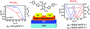
Two novel diketopyrrolopyrrole (DPP) small molecules DPPTT-F and DPPTT-H were synthesized. With the change of substituent from hexyl to perfluorohexyl, the HOMO and LUMO energy levels of DPPTT-F lowered, but the bandgap of DPPTT-H and DPPTT-F was nearly the same, which was proved by absorption spectra and electrochemistry. Thin film transistor characteristics showed DPPTT-H exhibited p-channel behavior with a hole mobility of about 0.2 cm2 V−1 s−1, while DPPTT-F displayed ambipolar characteristics with balanced hole and electron mobility in air. The mobility of DPPTT-F was 0.012 cm2 V−1 s−1 for holes and 0.011 cm2 V−1 s−1 for electrons. The microstructure and morphology of the thin films were also investigated. All these results demonstrated the unique property of perfluoroalkyl chains and their potential application in high performance organic ambipolar semiconductors.
Diketopyrrolopyrrole (DPP) has a fused planar structure and is an excellent building block for high performance polymer semiconductors.8–11 Recently, DPP based small molecules have captured attention owing to their well defined structure and promising charge transport performance.12–16 For instance, vacuum deposited thin films of DPP derivative 1a (Scheme 1) showed a high hole mobility of 0.7 cm2 V−1 s−1 and a current on/off ratio of 106 under ambient conditions.14 Till now, most of the reported DPP based small molecules exhibited p-channel behaviour; ambipolar materials are rarely reported and most of them are measured under vacuum or in inert atmosphere. Compound 1b (Scheme 1) displayed one of the highest ambipolar performances among DPP based small molecules with balanced electron and hole mobilities of about 10−3 cm2 V−1 s−1 in a vacuum by using Au as source and drain electrodes.16
It is well known that the fluorine-contained substituents can effectively lower the energy level of molecules and influence their orientation in the solid state, and thus affect the charge-transport behavior of materials.17–20 However, no much attentions has been paid to fluorine-containing DPP based small molecules. Y. Suna firstly introduced fluorine substituents into DPP based small molecules and synthesized compound 1c (Scheme 1).20 Thin film transistors of 1c displayed ambipolar characteristics. Though the performance of 1c was not high (electron mobility: 10−4 cm2 V−1 s−1, hole mobility: 10−5 cm2 V−1 s−1), it can be operated in ambient condition which is crucial to fabricate ambipolar transistors easily with low cost. Herein, two novel DPP derivatives DPPTT-F and DPPTT-H (Scheme 2) were successfully synthesized. Both compounds have same conjugation backbone, but their alkyl chain substituents are different. The alkyl chain substituents are hexyl for DPPTT-H and perfluorohexyl for DPPTT-F. Absorption spectra and electrochemistry results showed the replacement of hexyl with perfluorohexyl lowered the HOMO and LUMO energy levels of DPPTT-F, but the HOMO–LUMO energy bandgaps of DPPTT-H and DPPTT-F were nearly the same. Thin film transistor characteristics showed DPPTT-H exhibited p-channel behavior with hole mobility about 0.2 cm2 V−1 s−1, while DPPTT-F based transistors showed ambipolar properties with balanced hole and electronic mobilities in air. The maximum hole and electron mobility of DPPTT-F were 0.012 cm2 V−1 s−1 and 0.011 cm2 V−1 s−1, respectively, one of the highest value for DPP based ambipolar transistors in air. Their thin film microstructure and morphology were also investigated.
The UV-vis absorption spectra of DPPTT-H and DPPTT-F in o-dichlorobenzene solution and on thin films are shown in Fig. 1. Both compounds have strong absorption in the range of 460–780 nm in solution. Though perfluorohexyl chain has stronger electron withdrawing ability than that of hexyl group, surprisingly DPPTT-H and DPPTT-F displayed nearly the same absorption spectra in the solution, suggesting the replacement of perfluorohexyl group does not affect the HOMO–LUMO energy gap of the molecules. The optical energy gap estimated from solution spectra is about 1.89 eV. Comparing with that of solution, the absorptions of DPPTT-H and DPPTT-F based thin films were largely blue shifted. The maximum absorptions of DPPTT-H and DPPTT-F were blue shifted ∼113 nm and 76 nm respectively, indicating strong intermolecular interactions exist in the solid state. Additionally, a shoulder absorption at 630 nm for DPPTT-H and at 650 nm for DPPTT-F was observed, suggesting both compounds form H-type aggregation in the solid state.
The cyclic voltammagrams (CV) of DPPTT-H and DPPTT-F were measured in o-dichlorobenzene solution with 0.1 M Bu4NPF6 as electrolyte, Pt electrode as working electrode, and ferrocene as internal standard (Fig. 1b). DPPTT-H showed three reversible redox peaks, and the first reduction and oxidation potentials estimated from the midpoint of forward and backward scan are −1.18 V and 0.76 V respectively. The CV of DPPTT-F displayed non-reversible redox behavior, which might be ascribed to the effect of perfluorohexyl groups and the low solubility of DPPTT-F. The first oxidation and reduction peaks of DPPTT-F are at 0.98 V and −1.05 V. The HOMO/LUMO energy levels calculated from CV are −5.03/−3.09 eV for DPPTT-H and −5.25 eV/−3.22 eV for DPPTT-F. The HOMO–LUMO energy bandgap estimated from electrochemistry is 1.92 eV for DPPTT-H and 1.97 eV for DPPTT-F, close to the optical bandgap calculated from UV. Apparently, the perfluorohexyl groups lower the HOMO and LUMO energy levels of DPPTT-F, but nearly has no influence on its HOMO–LUMO energy bandgap.
In order to investigate the charge transport property of DPPTT-H and DPPTT-F, top-contact, bottom gate transistors were fabricated. The mobility of devices was calculated in saturation regime according to the expression IDS = (W/2L)μ × Ci (VG − VTh)2, where L and W are the channel length and width, respectively; Ci is the capacitance. Fig. 2 shows the typical transfer and output curves of DPPTT-H and DPPTT-F based transistors, and their device performance is summarized in Table 1. DPPTT-H exhibited p-channel behavior, and the highest hole mobility could reach ∼0.2 cm2 V−1 s−1 with Ion/Ioff ratio >104 at substrate temperature (Tsub) = 25 °C. When the Tsub was increased to 55 °C, the mobility of the devices was nearly no changed and the threshold voltage was slightly increased. Further increasing the Tsub to 85 °C, the mobility of the devices decreased to 0.03 cm2 V−1 s−1. DPPTT-F based transistors displayed ambipolar characteristic in air. The hole and electron mobility was 6.6 × 10⁻⁵ and 4.9 × 10⁻³ cm2 V−1 s−1 at Tsub = 25 °C respectively. Unlike DPPTT-H, with the increase of Tsub, the performance of DPPTT-F increased. The highest performance was observed at Tsub = 55 °C, balanced hole and electron mobility up to 10−2 cm2 V−1 s−1 was achieved, one of the highest value for DPP based small molecular ambipolar semiconductors in ambient condition. Absolutely, the perfluorohexyl chains should be responsible for the different electrical behaviors of DPPTT-H and DPPTT-F. Moreover, DPPTT-F based ambipolar transistors can be operated in air though the LUMO energy level of DPPTT-F is −3.22 eV, further demonstrating the unique property of perfluoroalkyl chains and their potential applications in high performance organic ambipolar semiconductors. In addition, the low optimized substrate temperature (55 °C) guarantees the potential applications of these compounds in flexible transistors.
DPPTT-H | DPPTT-F | |||||
---|---|---|---|---|---|---|
Tsub [°C] | μmax (μaver) [cm2 V−1 s−1] | Ion/Ioff | VT [V] | μmax (μaver) [cm2 V−1 s−1] | Ion/Ioff | VT [V] |
25 | 0.20 (0.15) | 5.3 × 10⁴ | −7 | 6.6 × 10⁻⁵ (6.5 × 10⁻⁵) (h) | 1.1 × 10² (h) | −30 (h) |
4.9 × 10⁻³ (1.4 × 10⁻³) (e) | 3.6 × 10³ (e) | 20 (e) | ||||
55 | 0.19 (0.17) | 4.0 × 10⁴ | 15 | 1.2 × 10⁻² (5.0 × 10⁻³) (h) | 4.6 × 10³ (h) | −72 (h) |
1.1 × 10⁻² (4.6 × 10⁻³) (e) | 8.4 × 10³ (e) | 70 (e) | ||||
85 | 3.8 × 10⁻² (3.0 × 10⁻²) | 2.2 × 10⁵ | −30 | 2.7 × 10⁻⁴ (8.5 × 10⁻⁵) (h) | 5.0 × 10² (h) | −55 (h) |
2.6 × 10⁻³ (1.3 × 10⁻³) (e) | 1.0 × 10⁴ (e) | 40 (e) |
The thin film quality, microstructure and morphology of DPPTT-H and DPPTT-F were investigated by X-ray diffraction (XRD) and atomic force microscopy (AFM). Fig. 3 illustrates the XRD patterns of the thin films deposited at different substrate temperatures. DPPTT-H thin films showed one diffraction peak when the Tsub was 25 °C and 55 °C respectively. The d-spacing estimated from XRD is 2.36 nm at Tsub = 25 °C and 2.59 nm at Tsub = 55 °C, suggesting DPPTT-H adopts different packing models on the substrate. Surprisingly, this changes has nearly no influence on the mobility and just slightly affected the threshold voltage of the devices, indicating both molecular packing models of DPPTT-H favorite charge transport. It is known the threshold voltage is strongly affected by the traps in the interfaces such as organic semiconductor – electrodes interface and organic semiconductor – dielectric layer interface, and in organic semiconductor thin film. We believe, more traps were formed in the devices at Tsub = 55 °C, which led to the increase of the threshold voltage. No peaks were observed for the films deposited at 85 °C, indicating its less crystalline and being consistent with the device performance. For DPPTT-F thin films, a series of single family diffraction peaks were observed. With the increase of substrate temperature, the intensity of the peaks increased, indicating the improved crystalline of the films. The d-spacing estimated from the first diffraction peak is 2.33 nm, close to that of DPPTT-H thin film deposited at Tsub = 25 °C. Fig. 4 shows the AFM images of DPPTT-H and DPPTT-F thin films. With increasing the substrate temperature from 25 °C to 55 °C, the grain size of DPPTT-F increased, and the grain boundaries became larger. While the substrate temperature increased to 85 °C, the grain size as well as grain boundary further increased, and the continuity of the film became worse. The thin films with large grain sizes and short grain boundaries facilitate charge transport. The large grain boundary might be responsible for the deteriorated device performance of DPPTT-F at Tsub = 85 °C. The morphology of DPPTT-H thin films exhibited the same tendency as that of DPPTT-F with the increase of substrate temperature. The different crystalline and morphology of the thin films led to the performance variation of DPPTT-H and DPPTT-F films at different substrate temperatures.
![]() | ||
Fig. 3 X-Ray diffraction of DPPTT-H and DPPTT-F films deposited on OTS modified Si/SiO2 substrates at different substrate temperatures. The wavelength for the X-ray source is 0.154 nm. |
![]() | ||
Fig. 4 AFM images of DPPTT-H (4 × 4 μm2) and DPPTT-F (3 × 3 μm2) thin films deposited on OTS modified Si/SiO2 substrates at different substrate temperature. |
Footnote |
† These authors contributed equally. |
This journal is © The Royal Society of Chemistry 2014 |