DOI:
10.1039/C3RA47408A
(Paper)
RSC Adv., 2014,
4, 16537-16544
Enhanced rectifying performance by asymmetrical gate voltage for BDC20 molecular devices
Received
11th December 2013
, Accepted 26th March 2014
First published on 27th March 2014
Abstract
By applying the asymmetrical gate voltage on the 1,4-bis (fullero[c]pyrrolidin-1-yl) benzene BDC20 molecule, we investigate theoretically its electronic transport properties using the density functional theory and nonequilibrium Green's function formalism for a unimolecule device with metal electrodes. Interestingly, the rectifying characteristic with very high rectification ratio, 91.7 and 24.0, can be obtained when the gate voltage is asymmetrically applied on the BDC20 molecular device. The rectification direction can be tuned by the different gate voltage applying regions. The rectification behavior is understood in terms of the evolution of the transmission spectrum and projected density of states spectrum with applied bias combined with molecular projected self-consistent Hamiltonian states analyses. Our finding implies that to realize and greatly promote rectifying performance of the BDC20 molecule the variable gate voltage applying position might be a key issue.
1 Introduction
In recent years, various molecular devices1–14 with interesting physical properties such as single-electron characteristic, negative differential resistance, molecular rectification, field-effect characteristics, and electronic switching have attracted considerable attention owing to their great potential practical applications in atomic-scale circuits. In particular, rectifying behavior7–14 is the fascinating aspect of the modern quantum transport phenomena because it is one of the most important electronic elements used for logic circuits and memory elements. So far, five aspects for a molecular rectification have been intensely studied: (i) an asymmetry in the coupling of a molecule to two identical electrodes;9,15 (ii) an asymmetry for a central electroactive unit placed inside a junction, for example, the central electroactive unit connected with alkyl chains of different lengths;10 (iii) an asymmetry of the electron density of the relevant molecular orbitals in the conjugated core, or D–σ–A molecular rectifier which was introduced by Aviram and Ratner based on a single organic molecule11 and has been widely studied;12 (iv) a conformational molecular diode, which depends on the molecule's orientation and displacement responding asymmetrically to the interelectrode applied field;13 and (v) asymmetrical Schottky barriers at both molecule–electrode contacts due to the difference in band structures of different electrode materials.16 Though rectification behavior has been found in a variety of molecular devices, unfortunately, the rectification efficiency of them is generally extremely low. Therefore, how to enhance the rectification efficiency of the molecular rectifier and obtain high-performance nanoscale rectifiers has been a focus of study in molecular electronics because the rectification ratio is a crucial parameter for the technical usefulness. Here, we suggest that another type of rectification can also be realized if the gate voltage is asymmetrically applied on the BDC20 molecular device. Yet, as far as we know, it is the first time for the realization in theory of the new molecular rectifier with high rectification ratio.
Manufacture of stable devices with wires fixed between electrodes requires “molecular alligator clips”. Much work has focused on the preparation of molecular wires incorporating thiol end-groups because these groups adhere strongly to gold.17 However, thiols are known to have many different binding sites on gold, which leads to fluctuations in the electronic properties of the molecular junction.18 We have turned our attention to using Buckminsterfullerene, as an anchoring group for obtaining a more well-defined contact region to gold. Recently, it has been investigated both experimentally19 and theoretically.20–22 Martin et al.19 have investigated the electrical characteristics of the C60 end-capped compound incorporated between two gold electrodes in a break junction. The studies revealed that in comparison to thiol anchoring, fullerene anchoring leads to a considerably lower spread in low-bias conductance. Furthermore, relevant experiments show that fullerene-anchored benzenes exhibited an increased stretching length before breaking.
As we all know, there are much more atoms in C60 than that in C20, which makes the self-consistent DFT calculations of electronic states calculation difficult and expensive in time. At the same time, considering that the electronic transport of C20 molecular device is similar with that of C60 molecular device.23,24 In order to reduce the computational cost, in this work, we study the transport through BDC20 molecule (see Fig. 1), in which a phenyl ring is connected to two C20 fullerenes25 on two opposite sides via a pyrrolidine group (in a so-called“dumbbell” fashion). Here, we consider applying a gate voltage on the different positions of BDC20 molecule. It should be possible to boost rectifying efficient because a gate voltage might greatly modify the electronic structure of such a molecule. Indeed, the currently reported very high rectification ratio, 91.7 and 24.0, employing the nonequilibrium Green's function method combined with the density functional theory (NEGF + DFT) calculations for a unimolecule connected with metal electrodes can be predicted when gate voltage is asymmetrically applied on the right C20 of the BDC20 molecule. Our findings highlight that asymmetrically gate voltage is an efficient way to realize a rectification behavior and the suitable gate voltage position is more important for greatly promoting rectifying characteristics and changing rectifying direction.
 |
| | Fig. 1 Structures of molecular devices in our simulation. The gray, white, blue and yellow spheres represent C, H, N and Au atoms, respectively. | |
2 Model and method
The molecular devices under study, as illustrated schematically in Fig. 1, are formed by the BDC20 molecule adsorbing onto two semi-infinite 3 × 3 Au (111) electrode surfaces directly, where bias voltage V is applied and the current is collect. Furthermore, an additional gate voltage is applied on the different regions of the molecule. Note that the gate electrode plotted in Fig. 1 is not a real physical electrode, and there is no current running from the source or drain electrode to the gate electrode. The electrostatic effect of the gate electrode in the experiment is simulated by shifting the molecular projected self-consistent Hamiltonian (MPSH) part of the Hamiltonian with the gate voltage. This shows that the gate electrode induces an external electrostatic potential on the molecular region.4,26 Systems with no gate voltage or only with gate voltage applied on the right C20, central phenyl ring (including pyrrolidine groups), central phenyl ring (including pyrrolidine groups) and right C20 molecule, and the whole BDC20 molecule are referred to as models M1 or M2, M3, M4 and M5, respectively. Model M1, M3 and M5 are the models with symmetrical gate voltage. Model M2 and M4 are the models with asymmetrical gate voltage. The purpose of forming five such different devices is to demonstrate asymmetrical gate voltage-modified effects on rectifying. To construct these molecular devices, each optimized molecular core by a separate calculation based on DFT is positioned between two Au (111) electrodes and is initially chosen to chemisorb to Au surface through bond contact. The distance between Au surface and C–C is 2.185 Å, which is a typical distance for the Au–C system.23 Each model is composed of three regions: the left electrode, the scattering region (the device region), and the right electrode. The scattering region contains molecular core and two layers of Au surfaces (18 atoms) on each side of molecule for screening the effects of the electrodes on molecule. The geometries are optimized until all residual forces on each atom are smaller than 0.05 eV Å−1.
The geometrical optimizations and the electronic transport properties are all calculated by the ATK package,4,27 which is based on the NEGF + DFT technique. In our calculations, the exchange-correlation potential is described by the generalized gradient approximation (GGA) in Perdew, Burke, and Ernzerhof (PBE) form.28 Valence electrons are expanded in a single-ζ plus polarization basis set (SZP) for Au atoms and a double-ζ plus polarization basis set (DZP) for C, N and H atoms. Core electrons are modeled with the Troullier–Martins nonlocal pseudopotential.29 The electrode calculations are performed under periodical boundary conditions, and the Brillouin zone has been sampled with 3 × 3 × 100 points within the Monkhorst–Pack k-point sampling scheme. We set 150 Ry as the cutoff energy for the grid integration and select 10−5 as the convergence criterion for the total energy. The nonlinear current through the device is calculated using the Landauer–Büttiker formula
| | |
I(V) = (2e/h)∫[f(E − μL) − f(E − μR)]T(E, V)dE,
| (1) |
where
h is the Planck's constant,
e is the electron charge,
f is the Fermi function,
V is the applied bias voltage,
μL and
μR are the electrochemical potential of the left and right electrodes, respectively,
Ef is the Fermi level of the system, which is set to be zero in our calculations, and
T(
E,
V) is the transmission function. The energy region contributing to the total current integral is called the bias window. In the approach, the molecular vibration effects have not been considered. Some deep discussions on these aspects in quantum transport can be found in
ref. 30.
3 Results and discussion
In Fig. 2, we present the dependence of current I on bias voltage V (I–V characteristics) in a bias region [−1.5 V, 1.5 V] for all five models we studied. In this figure, we can see obvious differences for these models due to the different applying position effects of gate voltage. Several important features in the I–V curves are clearly visible: For M1, M3 and M5, a symmetrical I–V curve arises as expected. The currents in M1 and M5 sustain small values in the low bias region and increase quickly at high bias. For M3, the current almost increases gradually with the increasing of the bias. For M4, the current rises rapidly and displays a linear behavior, representing an approximate Ohmic behavior under very small bias. And then the current drops dramatically with the increase of the bias and the current can be neglected in the [−0.7 V, −1.5 V] region, showing obvious asymmetry in current under positive and negative biases. This decrease in current due to an increase in bias is a manifestation of the negative differential resistance (NDR) behavior. Very interestingly, the I–V curve for M2 shows a highly asymmetric characteristic: the current rises rapidly from −0.3 to −0.6 V under negative bias and is almost quenched to zero in the region [−0.3 V, 0.0 V] and whole region of positive bias, which is very analogous to the I–V curve for a traditional diode, and thus a rather large rectification ratio can be expected.
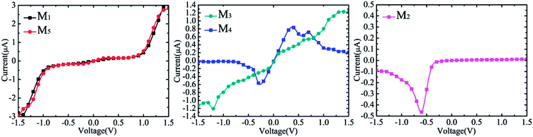 |
| | Fig. 2 I–V curves for all models. The I–V curve for M2 and M4 shows a highly asymmetric characteristic. | |
Fig. 3 shows the rectification ratio of five models. The rectification ratio, a ratio of the currents under negative and positive bias with the same voltage magnitude, can be calculated by R(V) = |I(−V)|/I(V). We define that the rectification ratio R(V) < 1[R(V) > 1] is the forward (reversed) rectification. Very interesting, two important physical phenomena can be observed from Fig. 3: (1) rectification directions are intimately related to the applying region of asymmetric gate voltage. We can observe significant reverse rectifying performances in M2 over our whole calculation region, and M4 shows a forward rectifying performance. (2) The rectification phenomenon depends strongly on the symmetry of gate voltage. There is no rectification phenomenon in M1, M3 and M5. Obviously, the electronic transport character of M2 presents the better rectifying effect than that of M4. The maximum values of rectification ratios are 24.0 at V = 0.8 V, and are far less than that for M2, 91.7 at V = 0.6 V. This is a currently reported very high rectification ratio with DFT calculations for a unimolecule device with metal electrodes and more than 30 times higher an original A-R diode.11 Other merits for M2 are its lower threshold bias, larger inverse current, and wider bias range for rectification. The gate voltage is symmetrical for M1, M3 and M5, and asymmetrical for M2 and M4. Therefore, it is reasonable to conclude that the asymmetry of gate voltage may be an effective way to promote rectifying performance and modulate the rectifying direction.
 |
| | Fig. 3 Rectification ratios change with bias for all models. | |
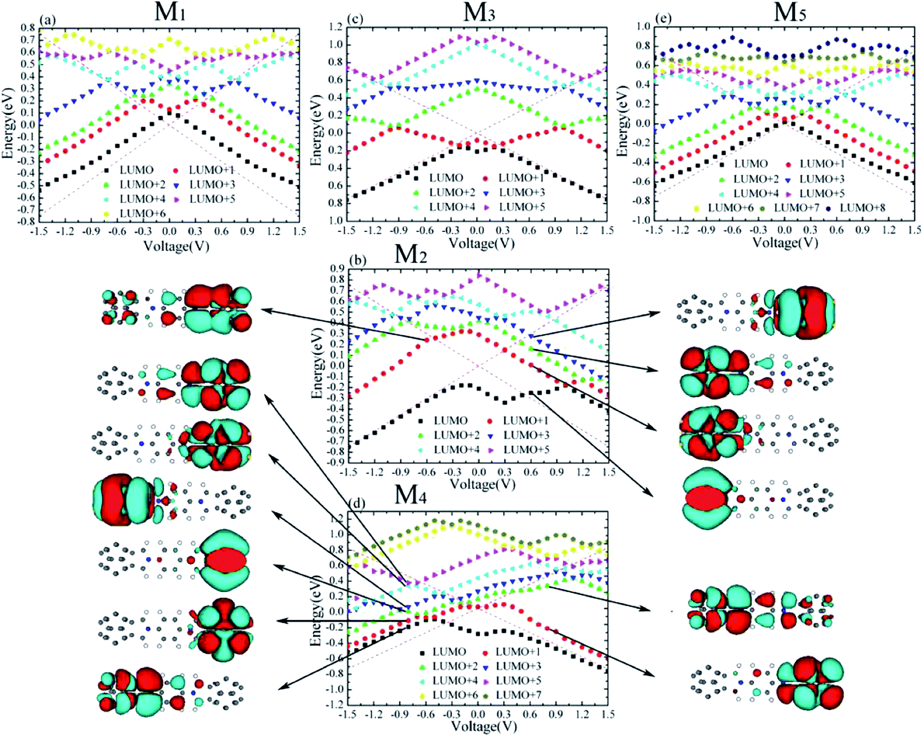
To make an analysis on rectifying mechanism, we calculate the spatial distribution of the MPSH12 for the frontier orbital levels at zero bias, which gives a visual description of the electronic structure and can be employed to predict qualitatively the small-bias rectifying behaviors, as shown in Fig. 4. MPSH state is the self-consistent eigenstate of the molecule in the presence of Au electrodes and thus it contains the molecule–electrode coupling effects during the self-consistent calculations. The highest occupied molecular orbital (HOMO) and the lowest unoccupied molecular orbital (LUMO) are defined as the level with a lower and higher energy position than the Fermi level at zero bias and zero gate voltage. The molecular orbitals shift when applying the gate voltage. For M1 and M5, HOMO and LUMO are closer to the Ef. For M2 and M4, LUMO and LUMO+1 are closer to the Ef. For M3, LUMO+1 and LUMO+2 are closer to the Ef. At zero bias, for M1 and M5, M2 and M4, and M3, HOMO and LUMO, LUMO and LUMO+1, LUMO+1 and LUMO+2 are the most important molecular orbitals for electronic transport, respectively, therefore their spatial distribution is a good indicator of molecular electronic structures. The spatial distribution of the MPSH for the frontier molecular orbitals in our five models is drawn in Fig. 4. The spatial distribution of these frontier orbitals is a good indicator of molecular electronic transportation.31 As can been seen, the frontier molecular orbitals for M2 and M4 tend to be localized, which contributes to the most asymmetry of I–V characteristics.32 For M1 and M5, the HOMO and LUMO state locate at the left and right C20 molecule, and pyrrolidine group area of the molecular device. For M3, the LUMO+1 state locate at the pyrrolidine group and central phenyl ring area. The LUMO+2 state mostly locates at the pyrrolidine group area. However, M2 and M4 are significantly different because the LUMO and LUMO+1 states locate at the left region (left C20 and pyrrolidine group) for M2 and at the left region (left C20 and pyrrolidine group), and the left region (left C20 and pyrrolidine group) and right C20, respectively, for M4. The higher the delocalization extension, the lower the barrier height, however, the less the asymmetry of the potential drop. For M1, M3 and M5, the spatial distribution of the MPSH for the frontier orbital levels is symmetrical, which has no contributions to a rectification under low bias. For M2 and M4, the spatial distribution of the MPSH for the frontier orbital levels is asymmetrical. This asymmetric spatial distribution of molecular states is the intrinsic origin for a rectification. The frontier orbital state in M2 has a stronger localization than that in M4, leading thus to a better rectifying performance for M2. Therefore, different transport behaviors, especially for a low bias, in various models can be expected due to different spatial distributions of molecular states.32–34
 |
| | Fig. 4 The composition of molecular orbitals for all models at zero bias. | |
In order to understand the observed rectification behavior over the whole calculated bias region, we plot transmission spectra of all models at various biases in steps of 0.2 V, as shown in Fig. 5, where the Fermi level is set to zero as stated before. The transmission spectra are the most intuitive representation of quantum transport behaviors. According to the Landauer–Büttiker formula, the current is determined by the integral area of transmission curve within the bias window (BW), which is the region [−V/2, V/2], considering the fact that Ef is set to be zero. From Fig. 5, one can see obvious dependence of the transmission spectra on the applied bias. When the bias is applied, the transmission peaks shift relative to the Ef and their strength is changed. For M1 and M5, the tunneling peaks move far away from the BW within ±1.2 V and the tunneling peaks under the positive energy shifts into the BW after exceeding around ±1.2 V under positive and negative bias. The case for M3 is similar to M1 and M5 except that a slight less transmission appears within the BW. M2 is special because the tunneling peak shifts into the BW after exceeding around −0.4 V under negative bias, and moves far away from the BW and disappears under positive bias. The strength of the tunneling peaks reduces drastically when the bias exceeds −0.6 V. Therefore, a large reverse rectification and NDR show up. For M4, the tunneling peak always stays inside (run into) the BW under positive bias, and stays outside the BW mostly within −0.2 V bias and disappears beyond −0.4 V bias, thus a forward rectification occurs. The strength of the tunneling peaks reduces drastically when the bias exceeds 0.4 V and −0.3 V, leading to a net drop in current and the onset of NDR at 0.4 V and −0.3 V. Here, modified effects on electronic structures by different position of voltage gate can be clearly observed.
 |
| | Fig. 5 Transmission spectra of all models at various biases in steps of 0.2 V. The red region denotes the bias window (BW). | |
As is well-known, in the transmission spectra, the position of the transmission peak is generally determined by the energy level of the MPSH orbital and the height of the transmission peak is dependent on the delocalization of the molecular orbital. It is worth noting that Fig. 4 is only related to zero-bias molecular states. When the bias is applied, a system is driven out of the equilibrium, and molecular levels should shift due to complicated reasons, such as the enhancement of molecular polarization and variations of the electrode potential, potential drop profile in the whole device region, and the bias-dependent coupling strength between a molecule and electrodes. Therefore, to understand the origins of these transmission peaks within the BW and their changes with the increase of bias, we give an evolution of the molecular orbitals with applied bias for all models, as shown in Fig. 6. For simplicity, the MOs which can enter into or go close to the BW are displayed. In Fig. 6, LUMO, LUMO+1, …, LUMO+6 for M1, LUMO, LUMO+1, …, LUMO+5 for M2, LUMO, LUMO+1, …, LUMO+5 for M3, LUMO, LUMO+1, …, LUMO+7 for M4, and LUMO, LUMO+1, …, LUMO+8 for M5, have a contribution to the current integral. As can be seen in Fig. 6(a), (c) and (e), the shift of the molecular orbitals within the BW under applied positive and negative bias is almost the symmetrical, so there are no rectifying performances for M1, M2 and M5. From Fig. 6(b) and (d), we can see the molecular levels within the BW show different shift tendency in the positive and reverse branches of the BW, which should affect the rectification ratio under various bias for M2 and M4. The asymmetric shift of frontier orbitals under bias35 is one of the key factors affecting the molecular rectification. To explore the origin of the asymmetric transmission spectra with respect to bias, we calculated the MPSH eigenstates. The isosurfaces of the MPSH eigenstates within the bias window for the M2 at V = −0.6 V and 0.6 V are plotted in the left and right panels of Fig. 6(b), respectively. At V = −0.6 V, LUMO+1 eigenstates are spatially delocalized throughout the whole molecule region, making a big contribution to the transmission spectrum featured by the big and wide peaks. In contrast, at V = 0.6 V, all of the four eigenstates (LUMO to LUMO+3) are localized in either the left region or the right region, which means that the channel is suppressed so that no transmission peaks pop up in the transmission spectrum curves. This difference accounts for the negative rectifying properties of M2. The isosurfaces of the MPSH eigenstates within the bias window for M4 at V = −0.8 V and 0.8 V are plotted in the left and right panels of Fig. 6(d), respectively. At V = −0.8 V, all the six eigenstates (LUMO to LUMO+5) are localized in either the left region or the right region. By contrast, one of the two eigenstates (LUMO+1 and LUMO+2) at V = 0.8 V are delocalized throughout the whole molecule region, causing the big and wide peaks in the transmission spectrum. As a result, the M4 shows a positive rectification behavior. Obviously, all of these are in agreement with those observed in Fig. 5 for transmission spectra. The above results indicate that the rectifying performance of M2 and M4 mainly results from the asymmetry distribution of the frontier MOs and the corresponding asymmetry evolution of the MO eigenenergies under the different direction of the external electric field, which is in agreement with previous predictions.12,35–38 Interestingly, asymmetrical gate voltage can strengthen this asymmetry (rectifying performance).
 |
| | Fig. 6 Evolution of the molecular orbitals with applied bias for all models. The MPSH states are plotted as left and right panels for each MO at certain biases. | |
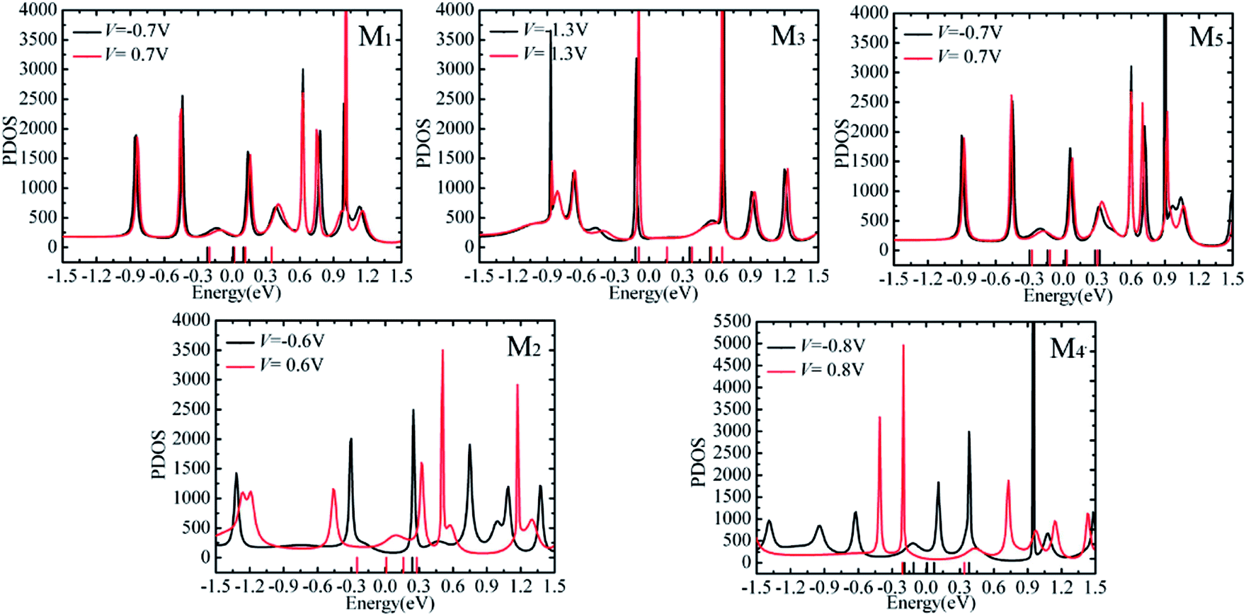
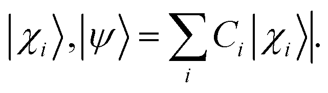
To understand the rectifying performance with more details, the projected density of states (PDOS) are calculated, as depicted in Fig. 7, for all models at several typical nonzero biases, corresponding to maximum values of rectification ratios. The orbital PDOS here is the density of states projected on the ith atomic basis orbital |χi〉, namely,
| |
 | (5) |
where |
ψ(
Enk)〉 is a wave function for the device scattering state and could be presented as a linear combination of the pseudoatomic basis orbitals
 Enk
Enk are energies of incident states of electrodes. More importantly, the bias-polarity dependence of PDOS can be clearly observed, which contributes to the rectification of a nanojunction. For M
1, M
3, and M
5, the PDOS are almost the same at positive and negative biases. In other words, no rectification in M
1, M
3, and M
5 can be expected. Nevertheless, M
2 and M
4 are entirely different; the PDOS peak in the vicinity of the Fermi level at negative bias is remarkably larger than that at positive bias. As a result, it has a best reverse rectification for M
2. There are two large PDOS peaks at positive bias near the Fermi level, which can greatly facilitate the electronic tunneling. As a result, it has a best forward rectification for M
4.
 |
| | Fig. 7 Device PDOS of all models at several typical nonzero biases. | |
To further rationalize the rectifying nature and profoundly understand the rectifying mechanism in essence, we plot the spatial distribution of the electrostatic difference potential for all models at zero biases, as shown in Fig. 8. Electrostatic difference potential is a solution to Poisson equation for the difference in electron density, which equals to the total density minus the neutral atom electron density. Generally speaking, for bulk hetero-junctions and molecular rectifiers, nonlinear drop of electrostatic potential occurs, and the region with high potential drop plays a dominate role in the rectification performance. Apparently, there exists a asymmetrical potential barrier in M2 and M4, which is an intrinsic origin of rectifying effect in our nanojunctions. While in M1, M3 and M5, the electrostatic difference potential distribution is symmetrical, thus there is no rectification. Note that the higher potential barrier appear at the right side of the scattering regions, as can be seen in M2. When M2 is positively biased, the electron tunneling is more favorable from the left electrode to right electrode. Consequently, the negative current is larger than the positive current and a reverse rectification occurs. The case M4 is extremely different from M2. It is just opposite for M4. Note that the higher potential occurs at the left side of the scattering regions, as demonstrated in M4. The electron transfer is more difficult from the left electrode to right electrode. A forward rectification can be expected accordingly.
 |
| | Fig. 8 The electrostatic difference potential distribution of all models at zero bias. | |
4 Conclusion
In summary, we have investigated the electronic transport properties of gated BDC20 molecular device by using the first-principle method based on the DFT combined with NEGF. We obtain a rectification ratio as high as 91.7 and 24.0 with a lower threshold bias, and wider bias range for rectification when the gate voltage is symmetrically applied on the right part of the BDC20 molecule. This is an interesting result. The analysis of the molecular projected self-consistent Hamiltonian and the evolution of the frontier molecular orbitals as well as transmission spectrum with various external voltage biases gives an inside view of the observed results, which suggests that rectifying performance are due to the asymmetry distribution of the frontier MOs and the electrostatic potential, and the difference of projected density of states spectrum with applied bias. Our finding implies that to realize rectifying characteristics of molecular device, the suitable applying position of gate voltage might be an effective way, which could be helpful in the field of large rectification ratio molecular devices.
Acknowledgements
This work was supported by the National Basic Research Program of China (Grant no. 2009CB929204), Natural Science Foundation of China (Grant no. 11074146 and 11374183), the Natural Science Foundation of Shandong Province (Grant no. ZR2010AM037 and ZR2012AQ018), the Excellent Youth and Middle Age Scientists Fund of Shandong Province (no. BS2012CL025) and the Independent Innovation Foundation of Shandong University (Grant no. 2009TS097 and 2012TS025).
References
- S. N. Rashkeev, M. D. Ventra and S. T. Pantelides, Phys. Rev. B: Condens. Matter Mater. Phys., 2002, 66, 033301 CrossRef.
- Z. H. Zhang, X. Q. Deng, X. Q. Tan, M. Qiu and J. B. Pan, Appl. Phys. Lett., 2010, 97, 183105 CrossRef PubMed.
- Z. Q. Fan and K. Q. Chen, Appl. Phys. Lett., 2010, 96, 053509 CrossRef PubMed.
- M. Brandbyge, J. L. Mozos, P. Ordejon, J. Taylor and K. Stokbro, Phys. Rev. B: Condens. Matter Mater. Phys., 2002, 65, 165401 CrossRef.
- S. J. Tans, A. R. M. Verschueren and C. Dekker, Nature, 1998, 393, 49 CrossRef CAS PubMed.
- T. M. Perrine, R. G. Smith, C. Marsh and B. D. Dunietz, J. Chem. Phys., 2008, 128, 154706 CrossRef PubMed.
- I. I. Oleynik, M. A. Kozhushner, V. S. Posvyanskii and L. Yu, Phys. Rev. Lett., 2006, 96, 096803 CrossRef CAS.
- X. Q. Deng, J. C. Zhou, Z. H. Zhang, G. P. Tang and M. Qiu, Appl. Phys. Lett., 2009, 95, 103113 CrossRef PubMed.
- Z. Zhang, Z. Yang, J. Yuan and M. Qiu, J. Chem. Phys., 2008, 128, 044711 CrossRef CAS PubMed.
- P. E. Kornilovitch, A. M. Bratkovsky and R. S. Williams, Phys. Rev. B: Condens. Matter Mater. Phys., 2002, 66, 165436 CrossRef.
- A. Aviram and M. A. Ratner, Chem. Phys. Lett., 1974, 29, 277 CrossRef CAS.
- J. B. Pan, Z. H. Zhang, X. Q. Deng, M. Qiu and C. Guo, Appl. Phys. Lett., 2010, 97, 203104 CrossRef PubMed.
- A. Troisi and M. A. Ratner, Nano Lett., 2004, 4, 591 CrossRef CAS.
- M. Bütiker, Phys. Rev. Lett., 1986, 57, 1761 CrossRef.
- J. Taylor, M. Brandbyge and K. Stokbro, Phys. Rev. Lett., 2002, 89, 138301 CrossRef.
- J. B. Pan, Z. H. Zhang, K. H. Ding, X. Q. Deng and C. Guo, Appl. Phys. Lett., 2011, 98, 092102 CrossRef PubMed.
- K. Nørgaard, M. B. Nielsen and T. Bjørnholm, Functional Organic Materials, VCH-Wiley, Weinheim, Germany, 2007 Search PubMed.
- C. Li, I. Pobelov, T. Wandlowski, A. Bagrets, A. Arnold and F. Evers, J. Am. Chem. Soc., 2008, 130, 318 CrossRef CAS PubMed.
- C. A. Martin, D. Ding, J. K. Sørensen, T. Bjørnholm, J. M. van Ruitenbeek and H. S. J. van der Zant, J. Am. Chem. Soc., 2008, 130, 13198 CrossRef CAS PubMed.
- J. K. Sørensen, J. Fock, A. H. Pedersen, A. B. Petersen, K. Jennum, K. Bechgaard, K. Kilsa, V. Geskin, J. Cornil, T. Bjørnholm and M. B. Nielsen, J. Org. Chem., 2011, 76, 245 CrossRef PubMed.
- T. Markussen, M. Settnes and K. S. Thygesen, J. Chem. Phys., 2011, 135, 144104 CrossRef PubMed.
- S. Bilan, L. A. Zotti, F. Pauly and J. C. Cuevas, Phys. Rev. B: Condens. Matter Mater. Phys., 2012, 85, 205403 CrossRef.
- Y. P. An, C. L. Yang, M. S. Wang, X. G. Ma and D. H. Wang, J. Chem. Phys., 2009, 131, 024311 CrossRef PubMed.
- Z. Q. Fan, K. Q. Chen, Q. Wan, B. S. Zou, W. H. Duan and Z. Shuai, Appl. Phys. Lett., 2008, 92, 263304 CrossRef PubMed.
- K. D. Sattler, Handbook of Nanophysics: Clusters and Fullerenes, CRC Press, 2011 Search PubMed.
- X. Q. Shi, Z. X. Dai, X. H. Zheng and Z. Zeng, J. Phys. Chem. B, 2006, 110, 16902 CrossRef CAS PubMed.
- J. Taylor, H. Guo and J. Wang, Phys. Rev. B: Condens. Matter Mater. Phys., 2001, 63, 245407 CrossRef.
- J. P. Perdew, K. Burke and M. Ernzerhof, Phys. Rev. Lett., 1996, 77, 3865 CrossRef CAS.
- N. Troullier and J. Martins, Phys. Rev. B: Condens. Matter Mater. Phys., 1991, 43, 1993 CrossRef CAS.
- S. Alavi, B. Larade, J. Taylor, H. Guo and T. Seideman, Chem. Phys., 2002, 281, 293 CrossRef CAS.
- J. M. Seminario, A. G. Zacarias and P. A. Derosa, J. Phys. Chem. A, 2001, 105, 791 CrossRef CAS.
- J. W. Zhao, C. Yu, N. Wang and H. M. Liu, J. Phys. Chem. C, 2010, 114, 4135 CAS.
- Z. H. Zhang, Z. Yang, J. H. Yuan, H. Zhang, X. Q. Deng and M. Qiu, J. Chem. Phys., 2008, 129, 094702 CrossRef CAS PubMed.
- H. M. Liu, N. Wang, P. Li, X. Yin, C. Yu, N. Gao and J. W. Zhao, Phys. Chem. Chem. Phys., 2011, 13, 1301 RSC.
- X. Yin, H. Liu and J. Zhao, J. Chem. Phys., 2006, 125, 094711 CrossRef PubMed.
- R. Stadler, V. Geskin and J. Cornil, Adv. Funct. Mater., 2008, 18, 1119 CrossRef CAS PubMed.
- R. Stadler, V. Geskin and J. Cornil, J. Phys.: Condens. Matter, 2008, 20, 374105 CrossRef CAS PubMed.
- A. Staykov, D. Nozaki and K. Yoshizawa, J. Phys. Chem. C, 2007, 111, 11699 CAS.
|
| This journal is © The Royal Society of Chemistry 2014 |
Click here to see how this site uses Cookies. View our privacy policy here. 


 Enk are energies of incident states of electrodes. More importantly, the bias-polarity dependence of PDOS can be clearly observed, which contributes to the rectification of a nanojunction. For M1, M3, and M5, the PDOS are almost the same at positive and negative biases. In other words, no rectification in M1, M3, and M5 can be expected. Nevertheless, M2 and M4 are entirely different; the PDOS peak in the vicinity of the Fermi level at negative bias is remarkably larger than that at positive bias. As a result, it has a best reverse rectification for M2. There are two large PDOS peaks at positive bias near the Fermi level, which can greatly facilitate the electronic tunneling. As a result, it has a best forward rectification for M4.