First-principles calculations on structural, electronic properties of V-doped 2H-NbSe2
Lin Chena,
Changsheng Li*a,
Hua Tanga,
Hongping Li*a,
Xiaojuan Liub and
Jian Mengb
aSchool of Material Science and Engineering, Jiangsu University, Zhenjiang, 212013, P. R. China. E-mail: changshengliujs@gmail.com; hpli@mail.ujs.edu.cn; Tel: +86 511 8879 0268
bState Key Laboratory of Rare Earth Resources Utilization, Changchun Institute of Applied Chemistry, Chinese Academy of Sciences, Changchun, 130022, P. R. China
First published on 15th January 2014
Abstract
Doping strategy has been applied in lots of areas holding promising performance for many functions. Here, we systemically report the main trends in structural, electronic properties and chemical bonding for V doped into 2H-NbSe2 in two types of doping by means of the first-principles PBE-GGA calculations. To investigate the stability of the doped system with changing concentration of V atoms, 2 × 2 × 1, 3 × 3 × 1 and 4 × 4 × 1 2H-NbSe2 supercells have been taken into consideration. Results show that it is easier to be doped as the concentration of dopant V is lower and the substituted doping structure is more stable than that of the dopant embedded into the interlayer. In addition, it is found that the dopant V atom forms a covalent bond with the surrounding Se atoms in both of the two doping structures, which can explain the variations of the structural parameters after V atom is doped into 2H-NbSe2. Moreover, what leads to the variation of the electronic structures is that the asymmetric structure and the more energetic Se atoms firstly near the dopant V atom after V is doped into 2H-NbSe2 in both of the two doping types. Our calculation results can provide good theoretical knowledge for the subsequent experiments.
Introduction
During the past few years, two-dimensional layered materials have attracted considerable attention from researchers due to their remarkable physical properties and promising applications such as being the basis for superconductors,1 lubricants,2 battery systems,3 solar cells,4 thin-film transistors5 and so on. Recently, layered transition-metal dichalcogenides MX2 (M = Mo, W, Nb and X = S, Se) (LTMDs) have been confirmed as excellent objects for study of fundamental physics among two-dimensional materials and have been extensively discussed, showing promising properties in electrical,6 mechanical7 and optical devices.8 These LTMDs are formed by three atomic thick stacked on each other along the c-axis like the sandwich type and held together by weak van der Waals' forces, resulting in a low coupling constant between layers. And various polytypes (2H, 3R, 4H, 6H, etc.) are characterized through different stacking sequences.9 Despite their structural similarity, transition-metal dichalcogenides present a wide variety of electronic behaviors going from semiconductors (MoS2) to semimetals (TcS2) and real metals (NbSe2).10 However, it has been studied that the specific physical properties of LTMDs can be easily modified by low doping levels.11–13As far as we concerned, doping is one of effective ways to improve material performance in many research fields such as photocatalytic materials,14 lithium-ion battery materials,15 information materials,16 magnetic materials,17 etc. Over the past decades, a number of experimental and theoretical studies have been dedicated to modify LTMDs' properties through the doping method mainly due to the attractive results brought by the dopants. Wenjing Li et al.18 found that the friction coefficient of the base oil containing Mo-doped WSe2 nanolamellars was lower and more stable than that of pure WSe2 nanolamellars partly because the Mo–WSe2 nanoflakes with thinner and smaller morphologies could form a more stable tribofilm on the rubbing surface. Similarly, Xiaopeng Qin et al.19 have finished a research on the microstructure, mechanical and tribological of Ti-doped MoS2 composite coatings, which manifests the hardness and adhesion of the composite coatings reached its maximum within a certain range of Ti content and doped Ti improved the tribological properties of pure MoS2 as well. Recently, the infrared vibrational properties of Re-doped MoS2 nanoparticles have been investigated,20 showing that phonon lifetime reduces further while the phonon lifetime of pure 2H-MoS2 is similar to that of traditional polar semiconductors like GaAs, which is of importance for understanding carrier–phonon interactions in low-dimensional semiconducting nanomaterials. Besides, using first-principles calculations, Y. C. Cheng et al.21 proposed a two-dimensional diluted magnetic semiconductor that was monolayer MoS2 doped by transition metals such as Mn, Fe, Co, Zn, Cd, and Hg, providing a promising systems to explore two-dimensional diluted magnetic semiconductors. In particular, Kapildeb Dolui et al.22 have systematically studied the electronic and magnetic properties of doped MoS2 monolayers via the possible substitutional dopants at S/Mo site, which presents a high potential for inducing large carrier concentrations within the MoS2 monolayer in the form of both electrons or holes.
Most significantly, as to 2H-NbSe2, several efforts have been undertaken to obtain better performance by doping 2H-NbSe2 as well. 2H-NbSe2 is widely studied owing to its essentially anisotropic system in which low-temperature superconductivity (Tc ∼ 8.6 K) is combined with a second order transition into a phase with charge density waves (around 33 K).23–25 A. Prodan et al.26 investigated the surface superstructures in niobium diselenide intercalated by Cu, Co and Fe, which shows various intercalates fill selectively the available interstitial sites forming composition dependent superstructures with different stacking of the host crystals. M. Iavarone et al.27 used low temperature scanning tunneling microscopy and spectroscopy to study the effect of Co/Mn atomic impurities on the superconducting state of NbSe2 that they are embedded in. What's more, the effect of Te doping on superconductivity and charge-density wave in 2H-NbSe2 by Wang28 revealing that both the RRR value and Tc decrease monotonically with increasing Te content and the disorder induced by impurity Te is remarkable. Mohammed Kars et al.29 also did the research on the structures of two intercalation compounds Ge ∼ 0.2NbSe2 and Ge ∼ 0.3NbS2 by single crystal X-ray diffraction and electron microscopy, high resolution electron microscopy and X-ray microanalysis, resulting in some different superstructures and diffracted diffuse intensity.
All of these previous works mainly focused on the changes of superconductivity, CDW, photoemission or the variation of morphology by doping other atoms into 2H-NbSe2. But few papers study the changes of structural and electronic properties in pure 2H-NbSe2 through the strategy of doping using theoretical or experimental methods. Therefore, it's our aim that our calculations will provide predicted information for the future experimental studies on the fundamental properties of Nb1−xMxSe2 compound (M represents the other transition metal elements).
To our best of knowledge, vanadium is in the same main group elements with niobium, indicating that they are in same properties to some extent. Therefore, in this work, the variations of structural and electronic properties by doping V into pure 2H-NbSe2 have been systematically investigated through the first principle calculation. Besides, two kinds of doping have been taken into consideration during our research. One of the doping types is that one Nb atom is replaced by V atom, the other of which is that V is embedded into the interlayer position in 2H-NbSe2. Our results reveal that both of the two structures are relatively stable after V is doped in 2H-NbSe2 by two doping ways and the dopant V atom form covalent bonds with the nearest Se atoms. In a way, our calculation results can provide a good theoretical knowledge to the subsequent experimental studies.
Computational details
In this paper, we have performed density functional theory calculations using the Cambridge Sequential Total Energy Package Code (CASTEP),30 which is one of the software modules in Materials Studio. In the crystal periodic potential field, the multi-electron system is expressed in expansion by the plane wave function, adopting three dimensional periodic boundary conditions. In order to minimize the number of plane wave basis, ultrasoft pseudopotential31 is used to describe the interactions between the ion core and the valence electrons in the Vanderbilt form. The geometry optimization is carried out by using the Broyden–Fletcher–Goldfrab–Shanno (BFGS) routine before we calculate the properties of the systems. The electron–electron exchange correlation interaction is considered by the generalized gradient approximation (GGA) with the functional parameterized by Perdew, Burke, and Ernzerhof (PBE).32 The cut-off energy for the plan-wave expansion is set as 400 eV after many convergence tests. For the calculation of structural and electronic properties, Monkhorst–Pack 6 × 6 × 3 K-point mesh for Brillouin zone is fixed. All the atoms are not relaxed to their equilibrium position until the ultimate energy change on each atom is less than 1 × 10⁻⁵ eV, the Hellmann–Feynman force applied on each atom is less than 0.03 eV Å−1, the maximum stress allowed is 0.05 GPa and the maximum displacement allowed is 0.01 Å. The valence electronic configurations considered for atomic pseudopotential calculation are Nb: 4s24p64d45s1, Se: 4s24p4, V: 3s23p63d34s2.Results and discussion
During this research, the ideal 2H-NbSe2 has hexagonal crystal structure of spacegroup 194-P63/mmc with six atoms in primitive crystal cell, the experimental lattice parameters of which are a = b = 6.8892 Å, c = 12.5444 Å, α = β = 90°, γ = 120°.33 Similar to BN, MoS2, ZnO and other heterogeneous grapheme-like sheets, Nb atoms occupy one sublattice of the hexagonal sheet and Se atoms occupy the other. The supercell employed contains 24 atoms (Fig. 1(a)), which correspond to a (2 × 2 × 1) supercell of 2H-NbSe2. After the structure of the supercell 2H-NbSe2 is optimized, the lattice parameters have been relaxed to change a little, which shows a = b = 6.9072 Å, c = 12.8070 Å, α = β = 90°, γ = 120.065°. Compared with the experimental value of the 2H-NbSe2, our calculated lattice parameters overestimate slightly to the experimental one under consideration. What leads to this phenomenon is that the applications of conventional DFT approach have well-known shortcomings when it is applied to the treatment of electronic structure with partly filled valence d shells in some atoms.34–36 As to our studied systems, the larger about 2.15% discrepancy in our optimized lattice constant c is due to the well documented failure of local and semi-local approximations for the exchange–correlation to describe the van der Waals interactions. In spite of this, the optimized values are in good agreement with the previous theoretical results.37,38 Therefore, it turns out that all of our calculated parameters are of certain reliability.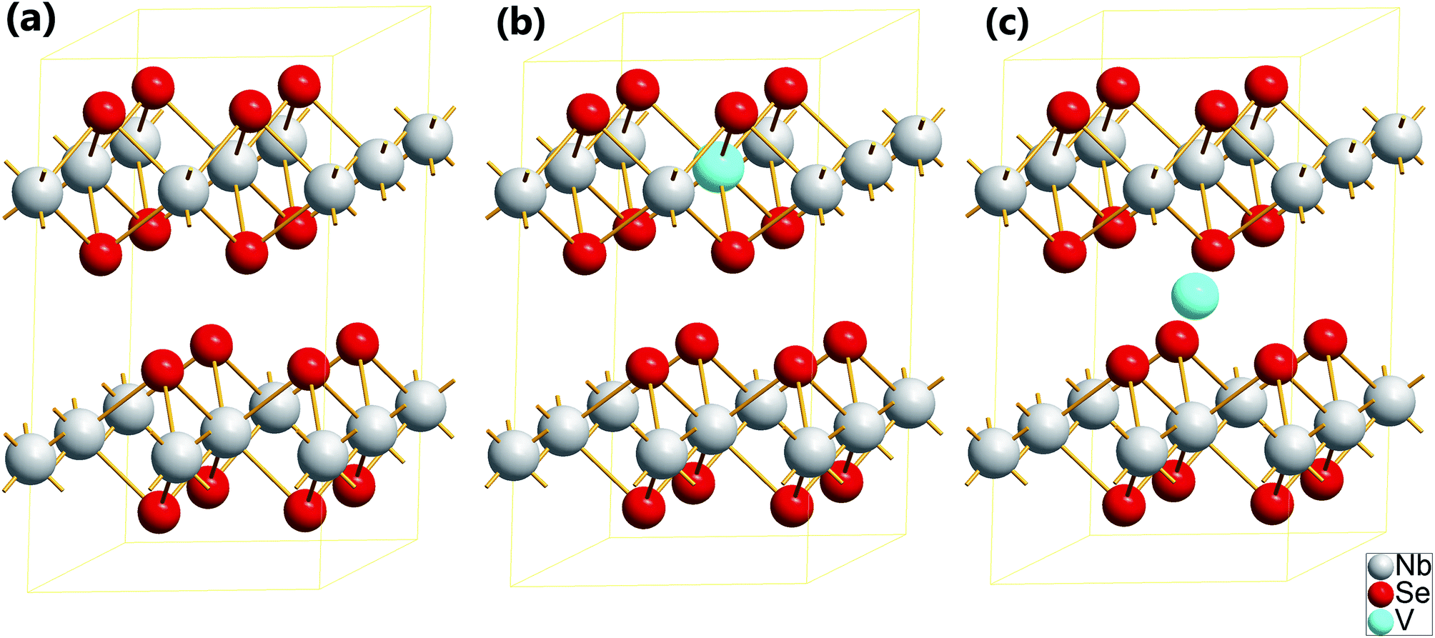 | ||
| Fig. 1 Two kinds of structures taken to be considered are showed in the perspective way. The atom symbols have been marked at the lower right corner in the picture. (a) The (2 × 2 × 1) supercell structure of pure 2H-NbSe2. As shown in the (a), 2H-NbSe2 consist of a layered hexagonal structure where the Nb atoms are sandwiched between Se atoms and the two adjacent NbSe2 layers rotate 180 degrees relatively. (b) The supercell structure of 2H-NbSe2 with one of Nb atoms replaced by a V atom (marked as RV-NbSe2). (c) The supercell structure of 2H-NbSe2 with a V atom embedded into the interlayer (marked as IV-NbSe2), In other words the doped V atom is in the octahedral interstice comprised of six Se atoms. | ||
As for doped systems, two types of doped systems are considered, one of which shows that single Nb atom is replaced by V atom marked as RV-NbSe2, the other of which describes that V atom is embedded into the interlayer position in the 2 × 2 × 1 2H-NbSe2 supercell marked as IV-NbSe2, as is shown in Fig. 1(b) and (c). After V is doped in the crystal structure of 2H-NbSe2 in two types as we adopted respectively, it brings about apparent variations of structure parameters and the surrounding atoms relaxed. Our calculated lattice parameters of the optimized supercell structures are summarized in Table 1. According to the data showed in Table 1, as V is doped into the structure 2H-NbSe2, the relaxing lattice parameters have changed, among which the parameter c of RV-NbSe2 increases obviously while it decreases in the system of IV-NbSe2 slightly. In the structure of RV-NbSe2, it has a tendency to extend along the c axis maybe because the ionic radius of V4+ atom (58 pm) is less than that of Nb4+ atom (68 pm) when the coordination number of V4+ is equal to that of Nb4+, which causes the Se atoms surrounding V locate closer to the V atom so that the distance between layer and layer becomes larger to a small extent. But in the structure of IV-NbSe2, the value of parameter c comes smaller, indicating that the interlayer V atom forms chemical bonds with the surrounding Se atoms which narrows the distance between layer and layer. And the variations of volumes of the two doped systems also prove this result well, showing that the volume of structure RV-NbSe2 is less than that of the pure 2H-NbSe2 and the volume of the structure IV-NbSe2 decreases a little compared with the pure 2H-NbSe2.
| Systems | a (Å) | b (Å) | c (Å) | c/a | α (°) | β (°) | γ (°) | V (Å3) |
|---|---|---|---|---|---|---|---|---|
| Pure | 6.907 | 6.907 | 12.807 | 1.854 | 90.000 | 90.000 | 120.065 | 528.806 |
| RV-NbSe2 | 6.867 | 6.867 | 12.837 | 1.869 | 90.000 | 90.000 | 120.000 | 523.921 |
| IV-NbSe2 | 6.901 | 6.901 | 12.748 | 1.847 | 89.929 | 90.070 | 119.967 | 525.951 |
To investigate the stability of the doped systems with different concentration of dopant V, 2 × 2 × 1, 3 × 3 × 1 and 4 × 4 × 1 2H-NbSe2 supercell, have been taken into consideration corresponding to the configurations Nb8Se16, Nb18Se36 and Nb32Se64, respectively. The formation energies of the two structures RV-NbSe2 and IV-NbSe2 were calculated according to the below schematic equation about the changes of matters after doping in the systems:
| E(RV-NbSe2)form = E(doped) − E(pure) − μV + μNb | (1) |
| E(IV-NbSe2)form = E(doped) − E(pure) − μV | (2) |
| Systems | Nb7VSe16 | Nb8VSe16 | Nb17VSe36 | Nb18VSe36 | Nb31VSe64 | Nb32VSe64 |
|---|---|---|---|---|---|---|
| Eform (eV) | −2.420 | −1.975 | −2.553 | −2.013 | −3.686 | −2.874 |
For understanding variations in the band structures due to different doping types of dopant V, the band structures of the undoped and doped models were calculated to the optimized structures. Fig. 2 presents the band structures in the first Brillouin zone along the high symmetry directions and Fig. 3 shows total and partial density of states of the three systems. The Fermi energy is defined as zero energy level. As shown in the Fig. 2(a) and 3(a), there exist four energy bands across the Fermi level as to pure bulk NbSe2 and the total density of states at Fermi energy is nonzero, which is accordant with the fact that NbSe2 is a good kind of conductor.38 Through Fig. 2(a) and 3(a), it can be seen that the band structure of pure 2H-NbSe2 is divided into two parts from -6 eV to 4 eV: the high energy VB and the low energy CB from −6 eV to 2 eV, which is mostly contributed by Nb 4d and Se 4p orbital electrons; the high energy CB from 2 eV to 4 eV, which is mainly offered by Nb 4d orbital electrons.
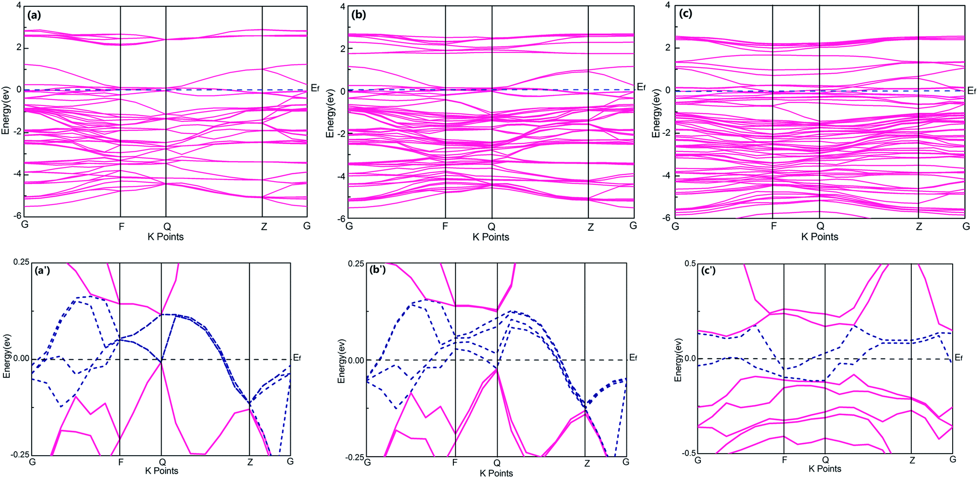 | ||
| Fig. 2 Band structure of: (a) pure 2H-NbSe2, (b) RV-NbSe2, (c) IV-NbSe2. The Ef represents the Fermi level, marked by the blue dashed line. The bands near Fermi level are magnified in additional figures (a′), (b′) and (c′) respectively. The dark blue dashed lines are the bands across Fermi level. | ||
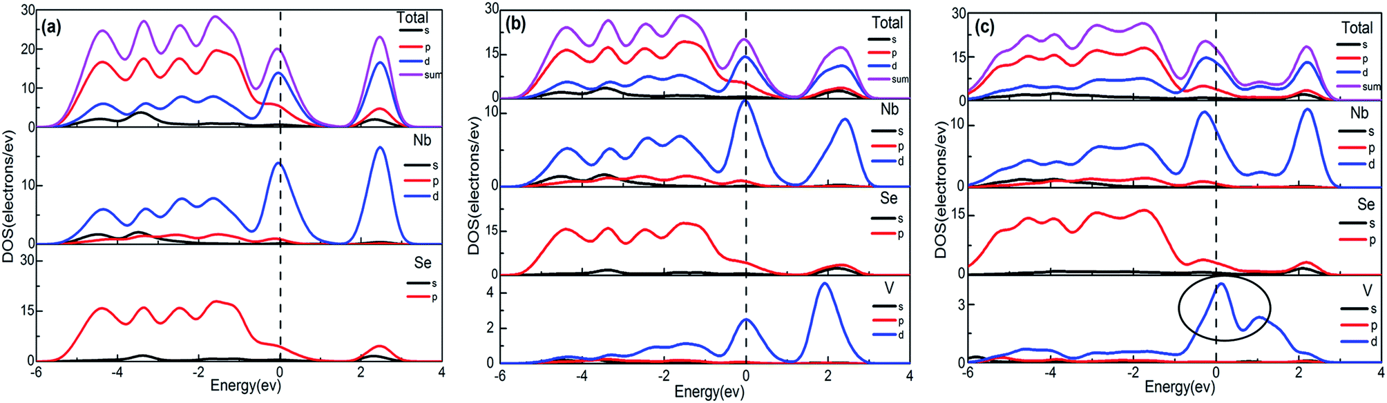 | ||
| Fig. 3 Total and partial DOS of: (a) pure 2H-NbSe2, (b) RV-NbSe2, (c) IV-NbSe2. PDOS near Fermi level of V in the system of IV-NbSe2 is marked with a circle in (c). Vertical dash line indicates Fermi level. | ||
Besides, Nb 4d orbital electrons play a major role on the Fermi energy and they have large density of states, which shows that the energy bandwidth around the Fermi energy is very narrow. In fact, the phenomenon is a fundamental feature among transition metal elements. Because of the discontent d shell of Nb, it will form discontent d energy band on the eye of the energy band theory. In addition, as Nb 4d orbital locates in internal orbital, there exist less overlaps between 4d orbital when Nb is combined to form a compound. Therefore, narrow energy bands around Fermi energy are formed. The PDOS of pure 2H-NbSe2 show that the main characteristic of the NbSe2 electronic structure is dominated by the hybridization between the transition metal-4d orbital and the Se-4p orbital, which is responsible for covalent Nb–Se bonds.
However it is nevertheless important to investigate the relative changes of electronic structure due to doping. As can be seen from Fig. 3, the band structures have changed after doping V in pure 2H-NbSe2 in a way. Compared with the band structure of pure 2H-NbSe2 in Fig. 2(a′), the number of the band across Fermi level remains four in the system of RV-NbSe2 (Fig. 2(b′)) while the number of the band during the high energy VB becomes more. And what we consider to explain that phenomenon is that the activity of Se atoms around the doping V atom becomes more reactive and the energy bands during the high energy VB come to split off because the coordination of V is less than that of Nb. This phenomenon can be seen from Fig. 4(a) and (b), which reveals that the partial density of Se atoms first neighbours of V has changed especially the four peaks during the high energy VB compared with the rest of Se atoms in the structure RV-NbSe2. Fig. 2(c) shows apparently the density of the energy bands becomes more in the structure IV-NbSe2. Just like what we mentioned before, the lattice of 2H-NbSe2 expands a little as to the system of IV-NbSe2, giving rise to the variation of the symmetrical characteristic of the lattice. Besides Fig. 4(c) also shows the partial density of Se atoms has changed a lot no matter what type of Se atoms compared with that of pure 2H-NbSe2. Therefore, the activity of the atoms in the system of IV-NbSe2 is improved and the energy bands come to split off more. As can be seen from Fig. 2(b), the separation gap between the high energy CB and the energy band cross Fermi level still exists like that of pure 2H-NbSe2 (Fig. 2(a)). But it disappears in the system of IV-NbSe2.
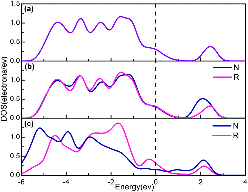 | ||
| Fig. 4 The partial density of Se atoms of: (a) pure 2H-NbSe2, (b) RV-NbSe2, (c) IV-NbSe2. The dark blue PDOS lines in (b and c) represent one of the Se atoms first neighbours of V and the red PDOS lines in (b and c) mean one of the rest Se atoms. | ||
In order to further understand the electronic structure of 2H-NbSe2 doped by V, it is necessary to understand the contribution of each atom in the density of states. The density of states and the partial density of states of the doped systems are shown in Fig. 3. It can be seen that the density of states on the Fermi level is mainly donated by Nb 4d and V 3d orbital electrons in the two doped systems, which are responsible for the metallic-like properties. Compared with the density of states and the partial density of states of pure 2H-NbSe2 (Fig. 3(a)), we find that the highest peak of Nb 4d shifts from 2.46 eV to −0.02 eV and proved from the nonzero total density of states between 0 and 2.5 eV of IV-NbSe2 (Fig. 3(c)). From −5 eV to Fermi level, V 3d and Se 4p attend to form the hybridization weakly, indicating that faintish V–Se covalent bond is formed.
To study the variation of chemical bonding induced by V doping respectively, the total charge density on the (110) surface for the four doping systems is shown in Fig. 5. The red color means a high charge density in these places while the dark green indicates the charge density is low. It is clear that the highest charge density resides in the immediate vicinity of the nuclei in both of the two systems. As can be seen from Fig. 5(a), the doped V atom and adjacent Se atoms form coordinate bonds from shared electrons and the overlap of V 3d orbital with Se 4p is less than that of Nb 4d orbital with Se 4p, indicating that the covalence of the Nb–Se bond is greater than that of V–Se bond. Nevertheless, Fig. 5(b) shows the (110) plane total charge density of the 2H-NbSe2 systems where V is embedded into the interlayer, from which we can qualitatively see the inserted V atom form covalent bonds with Se atoms nearby.
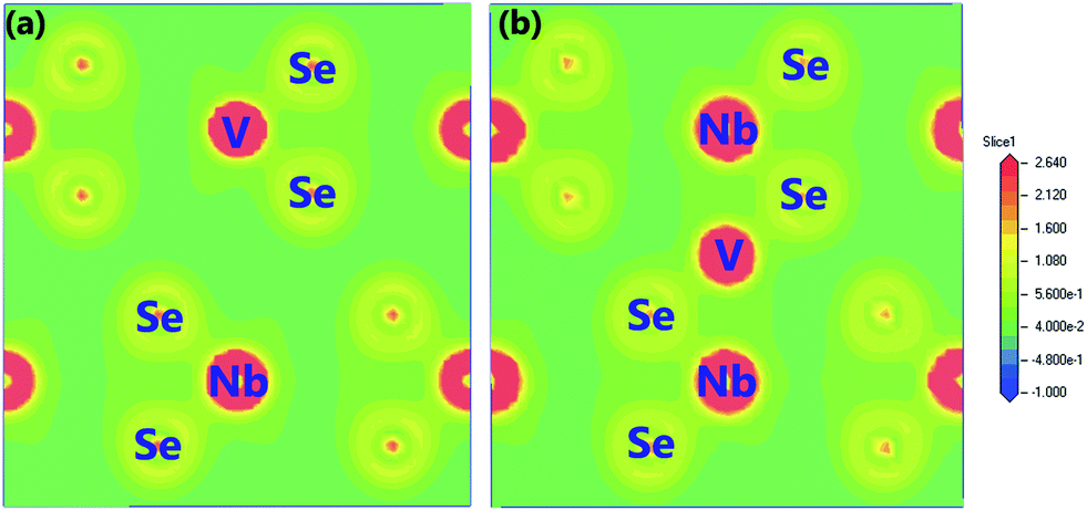 | ||
| Fig. 5 The (110) plane total charge density map of (a) RV-NbSe2, (b) IV-NbSe2. | ||
Conclusions
In summary, we have performed a systematic research on the structural and electronic properties of V doped into 2 × 2 × 1 2H-NbSe2 supercell (RV-NbSe2 and IV-NbSe2) by using Kohn–Sham Density Functional Theory. The calculation of formation energy shows it is easier to be doped as the concentration of dopant V is lower and the substituted doping structure is more stable than that of the dopant embedded into the interlayer. The four energy bands near Fermi level of NbSe2 are mainly dominated by Nb 4d orbital electrons and V 3d orbital electrons also make contributions to total density of states both in RV-NbSe2 and IV-NbSe2. Except the impurity bands caused by the doping atom, the energy bands during the high energy VB dominated partially by Se 4p orbital electrons come to split off, which explains the number of the high energy VB bands increases in the two doped systems. Furthermore, the (110) plane total charge density map of the two doped systems shows us the doped V atom forms covalent bonds with the nearest Se atoms. Our calculation results can provide a good theoretical knowledge to the subsequent experiments.Acknowledgements
This work was financially supported by National Natural Science Foundation of China (51275213, 21301075, 51372244, and 51302112), the Jiangsu National Nature Science Foundation (BK2011534, BK2011480), a Project Funded by Priority Academic Program Development of Jiangsu Higher Education Institutions, and Open Project of Key Laboratory of Tribology of Jiangsu Province (Kjsmcx2011002, Kjsmcx1005).Notes and references
- R. F. Frindt, Phys. Rev. Lett., 1972, 28, 299–301 CrossRef CAS.
- L. Rapoport, Y. Bilik, Y. Feldman, M. Homtonfer, S. R. Cohen and R. Tenne, Nature, 1997, 387, 791–793 CrossRef CAS PubMed.
- M. S. Whittingham, Science, 1976, 192, 1126–1127 CAS.
- H. Tributsch, Faraday Discuss. Chem. Soc., 1980, 70, 189–205 RSC.
- V. Podzorov, M. E. Gershenson, Ch. Kloc, R. Zeis and E. Bucher, Appl. Phys. Lett., 2004, 84, 3301–3303 CrossRef CAS PubMed.
- S. Bertolazzi, D. Krasnozhon and A. Kis, ACS Nano, 2013, 7, 3246–3252 CrossRef CAS PubMed.
- M. F. Cardinal, P. A. Castro, J. Baxi, H. Liang and F. J. Williams, Surf. Coat. Technol., 2009, 204, 85–90 CrossRef CAS PubMed.
- Y. G. Li, Y. L. Li, C. M. Araujo, W. Luo and R. Ahuja, Catal. Sci. Technol., 2013, 3, 2214–2220 CAS.
- F. Hulliger, Structural Chemistry of Layer-Type Phases, ed. F. A. Levy, Springer, 1976, Vol. 5, pp. 247 Search PubMed.
- J. A. Wilson and A. D. Yoffe, Adv. Phys., 1969, 18, 193–335 CrossRef CAS.
- V. L. Kalikhman, A. A. Golubnichaya, E. P. Gladchenko, V. K. Prokudina and L. P. Shchepinova, Powder Metall. Met. Ceram., 1982, 21, 801–803 CrossRef.
- V. V. Ivanovskaya, T. Heine, S. Gemming and G. Seifert, Phys. Status Solidi B, 2006, 243, 1757–1764 CrossRef CAS.
- V. V. Ivanovskaya, G. Seifert and A. L. Ivanovskii, Russ. J. Inorg. Chem., 2006, 51, 320–324 CrossRef.
- Y. M. Lin, Z. Y. Jiang, C. Y. Zhu, X. Y. Hu, X. D. Zhang, H. Y. Zhu, J. Fan and S. H. Lin, J. Mater. Chem. A, 2013, 1, 4516–4524 CAS.
- M. Y. Ge, J. P. Rong, X. Fang and C. W. Zhou, Nano Lett., 2012, 12, 2318–2323 CrossRef CAS PubMed.
- X. L. Su, W. C. Zhou, J. Xu, J. B. Wang, X. H. He, C. Fu and Z. M. Li, J. Am. Ceram. Soc., 2012, 95, 1388–1393 CrossRef CAS.
- K. Ueda, H. Tabata and T. Kawai, Appl. Phys. Lett., 2001, 79, 998–990 Search PubMed.
- W. J. Li, L. F. Hu, M. Z. Wang, H. Tang, C. S. Li, J. Q. Liang, Y. Jin and D. S. Li, Cryst. Res. Technol., 2012, 8(47), 876–881 Search PubMed.
- X. P. Qin, P. L. Ke, A. Y. Wang and K. H. Kim, Surf. Coat. Technol., 2013, 228, 275–281 CrossRef CAS PubMed.
- Q. C. Sun, D. Mazumdar, L. Yadgarov, R. Rosentsveig, R. Tenne and J. L. Musfeldt, Nano Lett., 2013, 13, 2803–2808 CrossRef CAS PubMed.
- Y. C. Cheng, Z. Y. Zhu, W. B. Mi, Z. B. Guo and U. Schwingenschlögl, Phys. Rev. B, 2013, 87, 100401(R) CrossRef.
- K. Dolui, I. Rungger, C. D. Pemmaraju and S. Sanvito, Phys. Rev. B: Condens. Matter Mater. Phys., 2013, 88, 075420 CrossRef.
- T. Yokoya, T. Kiss, A. Chainani, S. Shin, M. Nohara and H. Takagi, Science, 2001, 294, 2518–2520 CrossRef CAS PubMed.
- E. Boaknin, M. A. Tanatar, J. Paglione, D. Hawthorn, F. Ronning, R. W. Hill, M. Sutherland, L. Taillefer, J. Sonier, S. M. Hayden and J. W. Brill, Phys. Rev. Lett., 2003, 90, 7003–7006 CrossRef.
- C. D. Malliakas and M. G. Kanatzidis, J. Am. Chem. Soc., 2013, 135, 1719–1722 CrossRef CAS PubMed.
- A. Prodan, V. Marinkovic, M. Rojsek, N. Jug, H. J. P. van Midden, F. W. Boswell, J. C. Bennett and H. Bohm, Surf. Sci., 2001, 476, 71–77 CrossRef CAS.
- M. Iavarone, G. Karapetrov, J. Fedor, D. Rosenmann, T. Nishizaki and N. Kobayashi, J. Phys.: Condens. Matter, 2010, 22, 015501 CrossRef CAS PubMed.
- H. T. Wang, L. J. Li, D. S. Ye, X. H. Cheng and Z. A. Xu, Chinese Phys., 2007, 16, 2471–2475 CrossRef CAS.
- M. Kars, A. Gomez-Herrero, A. Rebbah and L. C. Otero-Diaz, Mater. Res. Bull., 2009, 44, 1601–1607 CrossRef CAS PubMed.
- M. C. Payne, M. P. Teter, D. C. Allen, T. A. Arias and J. D. Joannopoulos, Rev. Mod. Phys., 1992, 64, 1045–1097 CrossRef CAS.
- D. Vanderbilt, Phys. Rev. B, 1990, 41, 7892–7895 CrossRef.
- J. P. Perdew, K. Burke and M. Ernzerhof, Phys. Rev. Lett., 1996, 77, 3865–3868 CrossRef CAS.
- M. Marezio, P. D. Dernier, A. Menth and G. W. Hull Jr., J. Solid State Chem., 1972, 4, 425–429 CrossRef CAS.
- K. Terakura, T. Oguchi, A. R. Williams and J. Kubler, Phys. Rev. B, 1984, 30, 4734–4747 CrossRef CAS.
- C. Loschen, J. Carrasco, K. M. Neyman and F. Lllas, Phys. Rev. B: Condens. Matter Mater. Phys., 2007, 75, 035115 CrossRef.
- M. Cococcioni and S. de Gironcoli, Phys. Rev. B, 2005, 71, 035105 CrossRef.
- Y. G. Zhou, Z. G. Wang, P. Yang, X. T. Zu, L. Yang, X. Sun and F. Gao, et al., ACS Nano, 2012, 6, 9727–9736 CrossRef CAS PubMed.
- A. Kumar and P. K. Ahluwalia, J. Alloys Compd., 2013, 550, 283–291 CrossRef CAS PubMed.
| This journal is © The Royal Society of Chemistry 2014 |