 Open Access Article
 This Open Access Article is licensed under a Creative Commons Attribution-Non Commercial 3.0 Unported Licence
Electronic structure and band alignment of zinc nitride, Zn3N2
Su-Hyun Yooa,
Aron Walsh*b,
David O. Scanlonc and
Aloysius Soon*ad
aGlobal E3 Institute, Department of Materials Science and Engineering, Yonsei University, Seoul 120-749, Korea. E-mail: aloysius.soon@yonsei.ac.kr
bCentre for Sustainable Chemical Technologies, Department of Chemistry, University of Bath, Claverton Down, Bath BA2 7AY, UK. E-mail: a.walsh@bath.ac.uk
cKathleen Lonsdale Materials Chemistry, Department of Chemistry, University College London, 20 Gordon Street, London WC1H 0AJ, UK
dSchool of Physics, The University of Sydney, NSW 2006, Australia
First published on 3rd December 2013
Abstract
Zinc nitride (Zn3N2) is a promising candidate for optoelectronics applications due to its high electron mobility and high electrical conductivity. It is also thought that Zn3N2 can be used as a starting material to achieve p-type conductivity in ZnO-based oxide homojunctions. In this work, the electronic structure of bulk Zn3N2 is studied using density-functional theory (DFT) with different approximations to the exchange-correlation functional, ranging from (semi-)local functionals to the quasiparticle G0W0 approach. We predict a bandgap in the range of 0.9–1.2 eV, reconciling the scattered values reported in experiments, and a remarkably low work function (ionisation potential) of 4.2 eV for the (111) surface.
Introduction
For optoelectronic applications such as light emitting diodes (LEDs) and laser diodes, all-oxide homojunctions are very much desired and have distinct advantages over their hetero-counterparts, such as the prevention of heterojunction interfacial mismatch (resulting in lower efficiency), as well as reducing the high cost involved in the fabrication of semiconductor heterojunctions.In this aspect, zinc oxide (ZnO) is often considered as the choice material for the making of the oxide p–n homojunction, especially for ultraviolet UV/blue optoelectronic applications due to its wide bandgap energy of 3.437 eV (at 2 K) and large exciton binding energy, 60 meV.1 Unfortunately, due to the fact that the ZnO exhibits naturally strong n-type conductivity under the influence of native defects or adventitious donors, alternative ways to achieve p-type conductivity in ZnO are currently pursued by many researchers hoping to understand the fundamental physics to design and achieve robust p-type conductivity in ZnO.2–5
Recently, it has been proposed that a promising route to fabricate ZnO p–n homojunctions could be the transformation of zinc nitride (Zn3N2) into p-type ZnO by thermal treatment in oxidizing ambient conditions.6–8 The interest in Zn3N2 is also due to its intrinsic high electron mobility of 100 cm2 V−1 s−1 and as well as a high carrier concentration, 1020 cm−3.9 The low cost involved in the production of Zn3N2 also makes it an ideal choice for mass production in electronic systems. Both the binary zinc nitride system and the ternary zinc oxynitride mixture are composed of earth abundant elements, which makes them of further interest for solar energy harvesting. Control of the optical response, by varying the composition, could offer a route to low-cost, high-efficiency solar cells.
Unfortunately, as compared to ZnO, the fundamental bulk, surface and interface properties of Zn3N2 are poorly understood, possibly be due to the fact that Zn3N2 oxidizes rather easily under ambient conditions. Given the difficulty to study the properties of pristine Zn3N2, the true value of its intrinsic bandgap energy is still a matter of controversy, and reported values range from 1.0 to 3.2 eV.9–13 This current lack of understanding clearly hinders the further development of ZnO-based p–n homojunctions in devices.
In this letter, using density-functional theory (DFT), we will show that choice of the exchange–correlation (xc) functional is crucial in providing a consistent description of the electronic structure of Zn3N2. Semi-local functionals severely underestimate the bandgap energy and augmenting them with the Hubbard U model does not improve this shortcoming, while hybrid density-functionals provide the most consistent picture when compared to the many-body GW theory.
Computational approach
All calculations were performed using the Vienna Ab initio Simulations Package (VASP) code,14,15 employing a planewave basis set with an energy cutoff of 500 eV, within the projector augmented-wave (PAW) approach.16 In this work, the 40-atom primitive cell of Zn3N2 was used for all calculations, and the Brillouin-zone integrations were performed using a gamma-centered k-point grid of 4 × 4 × 4. The atomic geometry and electronic structure of bulk Zn3N2 was first calculated using the local-density approximation (LDA),17 the generalized gradient approximation (GGA) due to Perdew, Burke, and Ernzerhof (PBE),18,19 as well as the Hubbard U augmented forms of these approximations. For the LDA/GGA + U approach, various effective U values on the Zn 3d states were tested (ranging from 1 to 7 eV), and an optimal U of 5 eV was chosen. (See Appendix for more information) To further assess the accuracy of the electronic structure of bulk Zn3N2 within (semi-)local approximations, we have also performed electronic structure calculations using the modified Becke–Johnson meta-GGA20 due to Tran and Blaha (TB-mBJ),21 the HSE0622,23 and PBE024 hybrid functionals, as well as the perturbative quasiparticle G0W025, 26 approach performed on top of the HSE06 wavefunction.27Results and discussion
Zn3N2 is known to crystalize in the anti-bixbyite structure (space group of Ia![[3 with combining macron]](https://www.rsc.org/images/entities/char_0033_0304.gif) ), with a body-centered cubic lattice. The conventional cell of Zn3N2 has 80 atoms, as illustrated in Fig. 1a. The anti-bixbyite structure can be thought of as the calcium fluorite (CaF2) structure with N atoms occupying the cation sites, while the Zn atoms are located at three quarters of the anion sites. In this structure, the N atoms are coordinated to 6 neighbouring Zn atoms at 2 distinct sites represented by the 8b (1/4, 1/4, 1/4) and 24d (x, 0, 1/4) Wyckoff positions, as illustrated in Fig. 1b.
), with a body-centered cubic lattice. The conventional cell of Zn3N2 has 80 atoms, as illustrated in Fig. 1a. The anti-bixbyite structure can be thought of as the calcium fluorite (CaF2) structure with N atoms occupying the cation sites, while the Zn atoms are located at three quarters of the anion sites. In this structure, the N atoms are coordinated to 6 neighbouring Zn atoms at 2 distinct sites represented by the 8b (1/4, 1/4, 1/4) and 24d (x, 0, 1/4) Wyckoff positions, as illustrated in Fig. 1b.
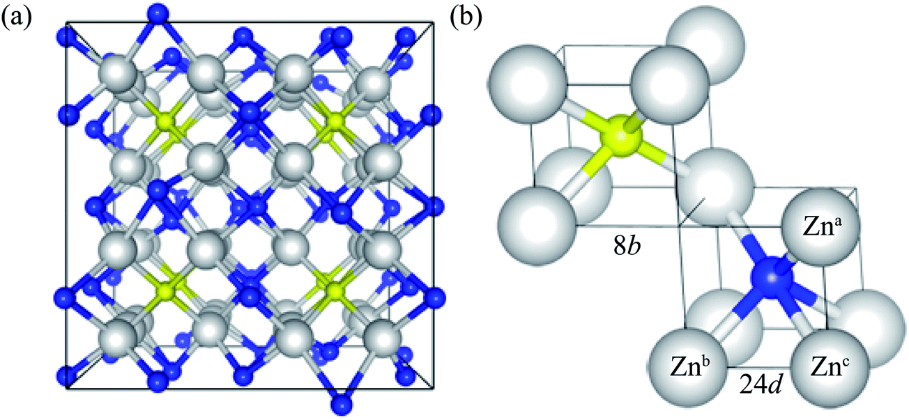 | ||
| Fig. 1 (Color online) (a) Perspective view of the atomic structure of bulk zinc nitride. (b) Spatial arrangement of zinc atoms around 2 distinct types of nitrogen atoms (denoted as 8b and 24d Wyckoff positions). The zinc atoms are represented as large white spheres, while the nitrogen atoms (8b and 24d) are shown as small yellow and blue spheres, respectively. | ||
Table 1 contains the calculated equilibrium lattice constant (neglecting zero-point vibrations) and the direct bandgap energy of Zn3N2 using various levels of approximations to the exchange-correlation density functional, as well as GW theory, in comparison to available experimental values.
The structural parameters calculated using PBE + U (9.692 Å), PBE0 (9.767 Å) and HSE06 (9.756 Å) provide the best agreement with the reported experimental value of 9.769 Å. The LDA and LDA + U values are clearly underestimated (up to 3.6%), while PBE overestimates it by about 1%. These are generally in line with analogous studies of other nitride materials.29–33 Thus, for the TB-mBJ and G0W0 calculations, structural parameters of bulk Zn3N2 were fixed to the values determined using HSE06 as those methods cannot currently be used for lattice optimisations.
Turning to the electronic structure of Zn3N2, we find that the values of the bandgap energy are just as scattered as those reported from experiments. Recent studies have shown that G0W0 generally has quantitative accuracy when describing the bandgaps of most (non-transition metal) semiconductors.34–37 In this sense, the calculated G0W0 bandgap energy value will be used as the benchmark and is found to be 1.15 eV. The calculations using LDA and PBE yield virtually a zero bandgap, with their Hubbard U counterparts improves it by about less than 0.5 eV, but still largely underestimated as compared to the G0W0 value. Both the HSE06 and PBE0 hybrid density-functionals further improve the bandgap energy with PBE0 overestimating it by about 0.5 eV. Interestingly, the recent meta-GGA functional, TB-mBJ gives a bandgap energy value of 0.95 eV which agrees the best with the G0W0 bandgap energy value. However, the band gap is just one relative energy difference from the full band structure and this agreement might not provide a fully consistent picture to the electronic structure of bulk Zn3N2. To illustrate this, we calculated and plot the electronic bandstructures of bulk Zn3N2 obtained by LDA, TB-mBJ, and HSE06 in Fig. 2.
 | ||
| Fig. 2 (Color online) The calculated electronic band structure of Zn3N2 obtained by (a) LDA, (b) TB-mBJ and (c) HSE06 density-functionals. The valence band edge is set to 0 eV. The conduction and valence bands are shown as yellow and blue lines, respectively. The bandgap energies calculated by TB-mBJ and HSE06 are 0.95 and 0.86 eV, respectively, whereas the bandgap energy by LDA is 0.03 eV. | ||
One challenge for electronic structure techniques applied to ZnO and related semiconductors is in the treatment of shallow core d states.38 Focusing on the relative position of the localized Zn 3d states in the sub-valence band (near −6 to −8 eV), it becomes apparent that the meta-GGA still fails to correct the level of Zn 3d states as predicted by the LDA (i.e. still too high with respect to the valence band maximum),39,40 albeit bringing the bandgap energy value closest to that by the G0W0 approach.41 On the other hand, using HSE06 which includes a percentage of the exact non-local Fock exchange, then reconciles the correct placement of the Zn 3d states.
Thus, we now proceed to further study the electronic structure of bulk Zn3N2 using the HSE06 density-functional with confidence that this level of theory will provide a balanced and consistent description of its electronic structure.
In Fig. 3a, we analyze the electronic density-of-states in three regions: (i) the sub-valence band (−9 to −6.5 eV), (ii) the upper-valence band (−6.5 to 0 eV), and (iii) the conduction band (above 0.86 eV). The sub-valence band finds a large contribution from the highly localized Zn 3d states, while the overlapping of the Zn 3d and N 2p states can be seen in the upper-valence band with the N 2p states more pronounced nearer the top of the valence band. The conduction band comprises of the empty Zn 4s and N 2s states. This corroborates well with the partial electron densities plotted for the states near the band edges in Fig. 3b and c.
 | ||
| Fig. 3 (Color online) (a) Electronic density-of-states for bulk Zn3N2. (b) 3D isosurfaces of the partial electron density of the states near the valence band edge and (c) that near the conduction band edge. These are calculated using the HSE06 density-functional. In (a), the valence band edge is set to 0 eV. The continuous lines indicate the contribution of Zn 3d (in blue) and 4s (in orange) states while the dashed lines represents the states of N 2p (in red) and 2s (in black). In (b) and (c), the Zn atoms are represented as large white spheres while the N atoms are shown as small blue spheres, respectively. | ||
Given that the physics of ZnO-based p–n homojunctions is a major research goal, as a first-step, it will be important to understand the relative band alignment of pristine ZnO and Zn3N2. In Fig. 4, we plot the natural valence band alignment based on our calculated ionisation potential of Zn3N2 and the previously calculated value for ZnO using the quantum mechanics/molecular mechanics (QM/MM) approach.42 This QM/MM approach has been shown to produce very accurate ionization potentials for materials, as it has direct access to the vacuum level.43 We calculated the ionisation potential for Zn3N2 using the slab model, adopting the standard approach as indicated by Van de Walle et al.44 First, a surface work function is determined by aligning the electronic band structure with respect to the vacuum level determined by a slab calculation of the stoichiometric (111) surface termination, which has no residual dipoles. The slab consisted of four quadrupolar layers (160 atoms). The natural band offset is thus the offset of the bulk ionisation potentials for each material, relative to the vacuum level. This alignment is free of any strain affects experienced at a true interface, and so represents a “natural band alignment” that would be seen between two unstrained materials.
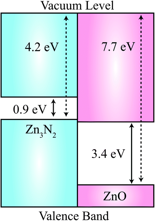 | ||
| Fig. 4 (Color online) Predicted band alignment between Zn3N2 and ZnO. The calculated work functions (ionization potentials) of Zn3N2 (HSE06) and ZnO (B97-1) are 4.2 and 7.7 eV, respectively, with their corresponding bandgap energies being 0.9 and 3.4 eV. | ||
The value of the HSE06-derived work function of Zn3N2 is 4.2 eV, which is aligned to the bulk ionisation potential using the core N 2p core level in the centre of the slab. The work function is remarkably low, e.g. for the photocatalytic oxide TiO2 has a value close to 8 eV.43 The natural value of 4.2 eV, places the valence band of Zn3N2 3.5 eV above that of ZnO, which results in a Type-IIB (misaligned) band offset.45 While it is generally expected that the valence band of the nitride would be higher in energy than an oxide due to the relative binding energy of the N 2p and O 2p atomic energy levels, this effect is exaggerated due to unusual octahedral coordination of N in Zn3N2 in contrast to the regular tetrahedral environments found for III–V semiconductors. The value is comparable to the new class of nitride electrode materials, which have work functions as low as 2.6 eV.46,47 We emphasise that the predicted natural band offset is representative of the two isolated systems, while for a synthesised heterostructure, interfacial effects (structural, compositional and electrostatic changes) could alter the Type-IIB behaviour.
Conclusions
In summary, we studied the electronic structure of bulk Zn3N2 systematically from the LDA to the many-body GW approach. We find that (semi-)local density-functionals (including the recent TB-mBJ functional) do not provide a consistent description of the electronic structure of bulk Zn3N2. The hybrid density-functional HSE06 provides the most consistent picture, yielding a bandgap energy value of 1 eV, close to that predicted by the G0W0 approach. The predicted work function of Zn3N2 is remarkably low, which is closer to alkaline earth nitrides than typical III–V materials. Future work should consider the interfacial structure of a ZnO/Zn3N2 composite and the effects of partial oxidation on the electronic structure.Appendix
Here we report the structural (in Table 2) and electronic properties (in Fig. 5) of Zn3N2, as calculated using the PBE + U approach. We tested different Ueff values, ranging from 0 to 7 eV, and benchmarked our results with that calculated using the HSE06 hybrid DFT functional for the electronic structure and available experimental results for structural properties.| Functional | Ueff (in eV) | Lattice constant | Zn–N1 | Zna–N2 | Znb–N2 | Znc–N2 |
|---|---|---|---|---|---|---|
| PBE + U | 0 | 9.857 | 2.144 | 2.015 | 2.065 | 2.329 |
| (0.90) | (0.52) | (0.95) | (−0.15) | (2.96) | ||
| 1 | 9.830 | 2.137 | 2.011 | 2.065 | 2.312 | |
| (0.62) | (0.19) | (0.75) | (−0.15) | (2.21) | ||
| 2 | 9.800 | 2.129 | 2.007 | 2.063 | 2.296 | |
| (0.32) | (−0.19) | (0.55) | (−0.24) | (1.50) | ||
| 3 | 9.768 | 2.121 | 2.002 | 2.061 | 2.278 | |
| (−0.01) | (−0.56) | (0.30) | (−0.34) | (0.71) | ||
| 4 | 9.733 | 2.112 | 1.997 | 2.058 | 2.262 | |
| (−0.37) | (−0.98) | (0.05) | (−0.48) | (0.00) | ||
| 5 | 9.695 | 2.103 | 1.991 | 2.054 | 2.244 | |
| (−0.76) | (−1.41) | (−0.25) | (−0.68) | (−0.80) | ||
| 6 | 9.653 | 2.093 | 1.984 | 2.049 | 2.227 | |
| (−1.19) | (−1.88) | (−0.60) | (−0.92) | (−1.55) | ||
| 7 | 9.605 | 2.081 | 1.975 | 2.043 | 2.209 | |
| (−1.68) | (−2.44) | (−1.05) | (−1.21) | (−2.34) | ||
| Exp.28 | 9.769 | 2.133 | 1.996 | 2.068 | 2.262 |
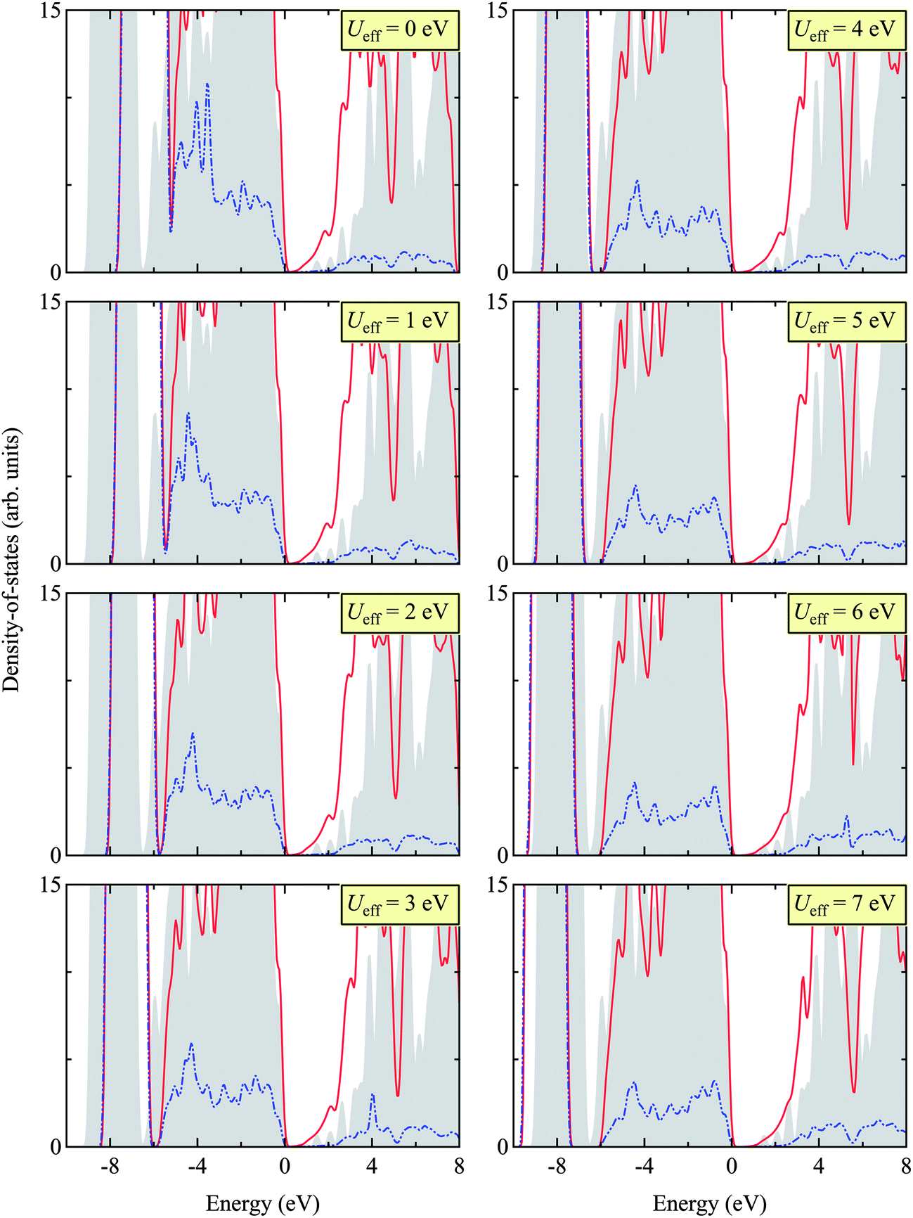 | ||
| Fig. 5 (Color online) Total (TDOS) and projected (PDOS) density of states for Zn3N2 calculated by HSE06 (as a benchmark) and PBE + U with different Ueff values (ranging from 0 to 7 eV). The gray shade indicates TDOS obtained using the HSE06 functional, the red line TDOS using the PBE + U approach, and the blue dotted line PDOS of Zn 3d states using the PBE + U approach. The valence band edge is set to 0 eV. The appropriate Ueff is then determined as 5 eV, matching the sub-valence band (near −8 eV) of HSE06 and PBE + U. We find this value of Ueff = 5 eV in close agreement with other Zn-based compounds, e.g. ZnO.48–50 | ||
Acknowledgements
We acknowledge membership of the UK's HPC Materials Chemistry Consortium, which is funded by the EPSRC Grant EP/F067496, and the Materials Design Network. Computational resources have also been provided by the KISTI supercomputing center (KSC-2012-C2-28, KSC-2013-C2-022). D.O.S. is grateful to the Ramsay Memorial Trust and the University College London for the provision of a Ramsay Fellowship. A.W. acknowledges support from the Royal Society. S.H.Y. and A.S. are supported by the National Research Foundation of Korea (NRF Grant no. 2011- 0013201) and the Global Frontier R&D Program (2013-073298) by the Ministry of Science, ICT & Future Planning, Korea.References
- D. C. Look, Mater. Sci. Eng., B, 2001, 80, 383 CrossRef.
- C. G. V. de Walle, Phys. Rev. Lett., 2000, 85, 1012 CrossRef.
- S. B. Zhang, S.-H. Wei and A. Zunger, Phys. Rev. B: Condens. Matter Mater. Phys., 2001, 63, 075205 CrossRef.
- W.-J. Lee, J. Kang and K. J. Chang, Phys. Rev. B: Condens. Matter Mater. Phys., 2006, 73, 024117 CrossRef.
- C. R. A. Catlow, A. A. Sokol and A. Walsh, Chem. Commun., 2011, 47, 3386 RSC.
- D. Wang, Y. C. Liu, R. Mu, J. Y. Zhang, Y. M. Lu, D. Z. Shen and X. W. Fan, J. Phys.: Condens. Matter, 2004, 16, 4635 CrossRef CAS.
- M. Bär, K. S. Ahn, S. Shet, Y. Yan, L. Weinhardt, O. Fuchs, M. Blum, S. Pookpanratana, K. George and W. Yang, et al., Appl. Phys. Lett., 2009, 94, 012110 CrossRef PubMed.
- N. H. Erdogan, K. Kara, H. Ozdamar, R. Esen and H. Kavak, Appl. Surf. Sci., 2013, 271, 70 CrossRef CAS PubMed.
- M. Futsuhara, K. Yoshioka and O. Takai, Thin Solid Films, 1998, 322, 274 CrossRef CAS.
- K. Kuriyama, Y. Takahashi and F. Sunohara, Phys. Rev. B: Condens. Matter Mater. Phys., 1993, 48, 2781 CrossRef CAS.
- K. Toyoura, H. Tsujimura, T. Goto, K. Hachiya, R. Hagiwara and Y. Ito, Thin Solid Films, 2005, 492, 88 CrossRef CAS PubMed.
- T. Suda and K. Kakishita, J. Appl. Phys., 2006, 99, 076101 CrossRef PubMed.
- G. Z. Xing, D. D. Wang, B. Yao, L. F. N. A. Qune, T. Yang, Q. He, J. H. Yang and L. L. Yang, J. Appl. Phys., 2010, 108, 083710 CrossRef PubMed.
- G. Kresse and J. Hafner, Phys. Rev. B: Condens. Matter Mater. Phys., 1993, 47, 558 CrossRef CAS.
- G. Kresse and J. Furthmüller, Phys. Rev. B: Condens. Matter Mater. Phys., 1996, 54, 11169 CrossRef CAS.
- G. Kresse and D. Joubert, Phys. Rev. B: Condens. Matter Mater. Phys., 1999, 59, 1758 CrossRef CAS.
- J. P. Perdew and A. Zunger, Phys. Rev. B: Condens. Matter Mater. Phys., 1981, 23, 5048 CrossRef CAS.
- J. P. Perdew, K. Burke and M. Ernzerhof, Phys. Rev. Lett., 1996, 77, 3865 CrossRef CAS.
- J. P. Perdew, K. Burke and M. Ernzerhof, Phys. Rev. Lett., 1997, 78, 1396 CrossRef CAS.
- A. D. Becke and E. R. Johnson, J. Chem. Phys., 2006, 124, 221101 CrossRef PubMed.
- F. Tran and P. Blaha, Phys. Rev. Lett., 2009, 102, 226401 CrossRef.
- J. Heyd, G. E. Scuseria and M. Ernzerhof, J. Chem. Phys., 2003, 118, 8207 CrossRef CAS PubMed.
- J. Heyd, G. E. Scuseria and M. Ernzerhof, J. Chem. Phys., 2006, 124, 219906 CrossRef PubMed.
- J. P. Perdew, M. Ernzerhof and K. Burke, J. Chem. Phys., 1996, 105, 9982 CrossRef CAS PubMed.
- L. Hedin, Phys. Rev., 1965, 139, A796 CrossRef.
- M. Shishkin and G. Kresse, Phys. Rev. B: Condens. Matter Mater. Phys., 2007, 75, 235102 CrossRef.
- N. Marom, F. Caruso, X. Ren, O. T. Hofmann, T. Körzdörfer, J. R. Chelikowsky, A. Rubio, M. Scheffler and P. Rinke, Phys. Rev. B: Condens. Matter Mater. Phys., 2012, 86, 245127 CrossRef.
- D. E. Partin, D. J. Williams and M. O'Keeffe, J. Solid State Chem., 1997, 132, 56 CrossRef CAS.
- T. Lee, B. Delley, C. Stampfl and A. Soon, Nanoscaele, 2012, 4, 5183 RSC.
- X. M. Duan and C. Stampfl, Phys. Rev. B: Condens. Matter Mater. Phys., 2009, 79, 035207 CrossRef.
- M. Fuchs, J. L. F. D. Silva, C. Stampfl, J. Neugebauer and M. Scheffler, Phys. Rev. B: Condens. Matter Mater. Phys., 2002, 65, 245212 CrossRef.
- Z. Li, P. Wang, H. Chen and X. Cheng, Physica B, 2011, 406, 1182 CrossRef CAS PubMed.
- R. Long, Y. Dai, L. Yu, M. Guo and B. Huang, J. Phys. Chem. B, 2007, 111, 3379 CrossRef CAS PubMed.
- H. Jiang, P. Rinke and M. Scheffler, Phys. Rev. B: Condens. Matter Mater. Phys., 2012, 86, 125115 CrossRef.
- X.-Z. Li, R. Gómez-Abal, H. Jiang, C. Ambrosch-Draxl and M. Scheffler, 2012, 14, 023006.
- M. A. L. Marques, J. Vidal, M. J. T. Oliveira, L. Reining and S. Botti, Phys. Rev. B: Condens. Matter Mater. Phys., 2011, 83, 035119 CrossRef.
- L. A. Burton and A. Walsh, Appl. Phys. Lett., 2013, 102, 132111 CrossRef PubMed.
- P. Rinke, A. Qteish, J. Neugebauer, C. Freysoldt and M. Scheffler, New J. Phys., 2005, 7, 126 CrossRef.
- D. J. Singh, Phys. Rev. B: Condens. Matter Mater. Phys., 2010, 82, 205102 CrossRef.
- H. Jiang, J. Chem. Phys., 2013, 138, 134115 CrossRef PubMed.
- D. Waroquiers, A. Lherbier, A. Miglio, M. Stankovski, S. Poncé, M. J. T. Oliveira, M. Giantomassi, G.-M. Rignanese and X. Gonze, Phys. Rev. B: Condens. Matter Mater. Phys., 2013, 87, 075121 CrossRef.
- A. A. Sokol, S. A. French, S. T. Bromley, C. R. A. Catlow, H. J. J. van Dam and P. Sherwood, Faraday Discuss., 2007, 134, 267 RSC.
- D. O. Scanlon, C. W. Dunnill, J. Buckeridge, S. A. Shevlin, A. J. Logsdail, S. M. Woodley, C. R. A. Catlow, M. J. Powell, R. G. Palgrave and I. P. Parkin, et al., Nat. Mater., 2013, 12, 798 CrossRef CAS PubMed.
- P. G. Moses, M. Miao, Q. Yan and C. G. Van de Walle, J. Chem. Phys., 2011, 134, 084703 CrossRef PubMed.
- P. Y. Yu and M. Cardona, Fundamentals of Semiconductors, Springer-Verlag, Berlin Heidelberg, 2010, vol. 4 Search PubMed.
- A. Walsh and D. O. Scanlon, J. Mater. Chem. C, 2013, 1, 3525 RSC.
- K. Lee, S. W. Kim, Y. Toda, S. Matsuishi and H. Hosono, Nature, 2013, 494, 336 CrossRef CAS PubMed.
- T. I. Lee, S. H. Lee, Y.-D. Kim, W. S. Jang, J. Y. Oh, H. K. Baik, C. Stampfl, A. Soon and J. M. Myoung, Nano Lett., 2012, 12, 68 CrossRef CAS PubMed.
- G.-Y. Huang, C.-Y. Wang and J.-T. Wang, Comput. Phys. Commun., 2012, 183, 1749 CrossRef CAS PubMed.
- Z. Wang, M. Zhao, X. Wang, Y. Xi, X. He, X. Liu and S. Yan, Phys. Chem. Chem. Phys., 2012, 14, 15693 RSC.
| This journal is © The Royal Society of Chemistry 2014 |