Mechanical properties and thermal stability of ultrathin tungsten nanowires

Ken-Huang Lina, Jia-Yun Lia, Jenn-Sen Linb, Shin-Pon Ju*a, Jian-Ming Lu*cd and Jin-Yuan Hsieh*e
aDepartment of Mechanical and Electro-Mechanical Engineering, National Sun Yat-sen University, Kaohsiung 804, Taiwan. E-mail: jushin-pon@mail.nsysu.edu.tw
bDepartment of Mechanical Engineering, National United University Miao-Li, 360, Taiwan. E-mail: jsenlin@nuu.edu.tw
cNational Center for High-Performance Computing, Tainan 744, Taiwan. E-mail: 0403817@narlabs.org.tw
dDepartment of Mechanical Engineering, Southern Taiwan University of Science and Technology, Tainan 710, Taiwan
eDepartment of Mechanical Engineering, Minghsin Institute of Technology, Hsin-Chu 304, Taiwan. E-mail: Jyhsieh@must.edu.tw

Received 29th October 2013 , Accepted 18th December 2013

First published on 20th December 2013


Abstract

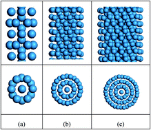
The most stable structures of three ultrathin tungsten nanowires were predicted by the simulated annealing basin-hopping method (SABH) with the penalty algorithm. The predicted structures of tungsten nanowires indicate the tungsten nanowires at this small scale do not possess the B.C.C. configuration in bulk tungsten material. By molecular dynamics (MD) simulation, the mechanical properties including the Young's modulus, yielding stress, and strength of these wires were determined by the tensile test after the analysis of the stress–strain profiles. Besides, in order to understand the feasibility of application of tungsten nanowire on nanodevices, the thermal stability of these ultrathin tungsten nanowires was also investigated at room temperature (300 K) by molecular dynamics (MD).


Introduction

In recent years, nanowires have been investigated widely because they possess broad applications in different areas, such as nano-mechanical1,2and nano-electronic devices.3 The metallic nanowires with well-defined structures of several nanometers have been fabricated by using different methods. As the scale decreases to nanometers, the nature of physical and transport phenomena will dramatically change due to the surface effect, small size effect and quantum effect.4–6 Tungsten is a brittle metal and possesses higher tensile strength; however, tungsten nanowires are ductile material at the nanoscale.4 Therefore, tungsten has great mechanical, chemical and electronic properties,1,7–9 could be used in different application. Huang10 investigated single crystal tungsten nanowire which found that the average yield stress was 8.44 GPa. Besides, the yield strength (3.4 to 5.8 GPa) are larger than bulk tungsten. Cimalla et al.11 used AFM to analysis different sizes tungsten nanowires from 100 nm to 300 nm, and they found that the Young's modulus is 332 GPa close bulk tungsten values. In addition, Li et al.12 using molecular dynamics simulations constructed 2.3 nm diameter tungsten nanowires to simulate mechanical energy storage methods, found that tungsten nanowires strain recovery can be greater than 30%, the maximum stress is 3500 MPa and energy storage efficiency is 98%. Those excellent nature properties possess better energy storage and applications than currently found smart materials.

Except for W nanowire research, some fundamental studies investigated the physical properties of metallic nanowires using the molecular dynamics simulation. For example, melting behavior in metal nanowires were carried out, and found that the interior melting temperature in ultrathin nanowires is lower than that of the surface melting. The mechanical behavior for the tensile test of the copper nanowires is studied.13 The strain rate effect induced by amorphizations of Ni nanowires has been investigated using molecular dynamics simulation.14

Due to tungsten nanowires has very excellent characteristics, in this study, we constructed different sizes nanowire and analyze the ultrathin nanowires mechanical properties. The structures of these ultrathin tungsten nanowires show as consisting of coaxial tube with n, n′, n′′, n′′′ helical atom rows, where n is the atom number of outer shell, n′ is of the first shell, and n′′ is second shell and so on. The radius of multi-shell tungsten nanowires are from 2.63 Å to 7.0 Å., Three types of nanowires are named 6-1, 11-6-1 and 16-11-6-1 W nanowire and the diameters are 2.63 Å, 5.0 Å and 7.0 Å, respectively. Significantly, the structures of the ultrathin tungsten nanowires are deferent from B.C.C. crystal, no matter in the mechanical, electronic and thermal properties.

Since the studies of W nanowire mechanical properties are still lacking, we examine their mechanical properties and deformation behavior of the 6-1, 11-6-1 and 16-11-6-1 multi-shell W nanowire via molecular dynamics (MD) simulation.

Simulation model

Up to now, many global optimization algorithms have been successfully developed to obtain such a favorable configuration, such as genetic algorithms (GA),15 the big-bang method (BB)16 and the simulated annealing basin-hopping (SABH)17 global optimization algorithm. In the present study, the multi-shell structure of the ultrathin nanowires had been constructed by SABH. In the traditional basin-hopping method, a conjugate gradient method was used to reach the local minimum, where a new geometry is generated. In our SABH method, the conjugate gradient method was replaced by the limited memory BFGS method (LBFGS),18 which can be used to simulate a system consisting of a large number of atoms. Furthermore, using the LBFGS method in the BH method is faster than the conjugate gradient method for a larger system. Furthermore, the simulated annealing18 (SA) method was also implemented with the BH method to be a SABH method, which includes a wider searching domain within the potential energy surface. Therefore, we adopt the LBFGS method in the SABH method to converge the system and reach the local minimum. Due to the searched configurations are near spherical in geometry in three-dimensional space, we use SABH to combine the penalty function for the one-dimensional nanowire structures.

The EAM19 and tight-binding potentials20 are two popular functions to describe the transition function and these two potentials are also developed to simulate alloy systems. Some material properties are predicted to simulate the alloy systems and presented dramatic results.21 However, the tight-binding many-body potential20 possesses the simple formula and could be save the more computational time. The interaction between two W atoms depends not only on the distance between them, but also on their local environment. The prediction of some properties by SABH method has proven to be more accurate for some transient metals in the past studies.20,22 This model commences by summing the band energy, which is characterized by the second moment of the d-band density of state, and a pairwise potential energy of the Born-Mayer type and is expressed in the following form:

 
image file: c3ra46215c-t1.tif(1)
where ξ is an effective hopping integral, rij is the distance between atom i and j, and r0 is the first-neighbour distance. The parameters of the tight-binding potential relating to W in current simulation are listed in Table 1.23 Furthermore, the interaction force on atom i is given by
 
image file: c3ra46215c-t2.tif(2)

Table 1 The bulk tight-binding potential parameters
  A (eV) ξ (eV) p q r0 (Å)
W 0.249 3.2055 10.3715 1.9916 2.741


In addition, the penalty function is adopted in the SABH method, which is used to constrain all atoms within a cylindrical space with a specific cross-section radius. The formula of the penalty method is shown as follows:

 
image file: c3ra46215c-t3.tif(3)
 
pi = [xi2 + yi2r02]2 (4)
where Ei is the energy of atom i calculated by TB potential, and pi is the penalty potential. pi is applied to atom i only if atom i is located outside the radius of nanowire (r0). The terms xi and yi are the coordinate of atom i in x and y directions, and c is defined to discriminate whether the atom is in the wire radius range. The value c = 200 was adopted in this SABH calculation. In fact, c is independent of final structure as long as the c value is large enough. The formula of the penalty potential can be defined as any form which provides a constraint condition of the simulation model.

We had combined SABH with penalty method to construct the ultrathin nanowires by different initial conditions. Furthermore, the optimizations are implemented by the density functional theory (DFT) calculation, and finally obtained three global minimum structures in this calculation progress. The number of 119, 400, and 500 W atoms are optimized with 250[thin space (1/6-em)]000 steps by LBFGS method are adapted to search the stable W nanowires. Then, the ordered segment of obtained W nanowires by SABH method is used to estimate the information of its unit cell. Three types of multishell structure, i.e., 6-1, 11-6-1, and 16-11-6-1 are shown in Fig. 1(a)–(c). For three types multishell configurations all have a single central strand of tungsten atoms and a tube structure formed the wires of atom coiled around the axis of the tube, they all could be presumed as a cannular type of nanowire.


image file: c3ra46215c-f1.tif
Fig. 1 The three types of W nanowires (a) 6-1, (b) 11-6-1, and (c) 16-11-6-1.

The loading state of the molecular dynamics simulation for the tensile test is as follows: the loading is applied along the axis, and top and bottom layers are set as fixed layers, and the others are set as thermal controlled layers. To keep the system temperature remaining constant during simulation, the Nosé–Hoover method is adopted to ensure a constant system temperature during the simulation process. The stress calculation in the atomistic simulation σmn on m plane and n-direction is calculated by

 
image file: c3ra46215c-t4.tif(5)
where mi is the mass of atom i; Vi is the volume assigned around to atom i; NS is the number of particles contained in the region S, and S is defined as the region of atomic interaction; Rij is the distance between atoms i and j; xmij and xnij are two components of the vector from atom i to j. The normal strain in the axial direction ε is calculated as
 
image file: c3ra46215c-t5.tif(6)
where image file: c3ra46215c-t6.tif is the average length in axial direction and lz(o) is its average initial length. Thus, the stress–strain relationship of the ultrathin tungsten nanowires could be yielded by means of the eqn (5) and (6).

Results and discussion

In this work, three types of multi-shell nanowires with different diameters have been constructed by simulated annealing basin-hopping method which adapts tight-binding potential. This study addresses tensile tests of ultrathin tungsten nanowires with the 6-1, 11-6-1, and 16-11-6-1 structures. To understand the width effect on the mechanical property and the deformation mechanism in this work, three different widths of W nanowires are equilibrium at 300 K for 50 ps. The calculated results of radius, cohesive energy, Young's modulus, yielding stress, yielding strain, and maximum strain for three types of nanowires are listed in Table 2. The radiuses of 6-1, 11-6-1, and 16-11-6-1 structures are 2.63, 5.0, and 7.0 Å, respectively. The stress–strain relationship is studied to stress to overcome the pre-compressive stress. Therefore, the yielding stress of the 6-1 structure is higher than that of the bulk structure. For clearly discussing the detail of the tensile behavior, a central region and prominent edge are defined for 6-1, 11-6-1, and 16-11-6-1 W nanowire in Fig. 2. The corresponding stress–strain profiles for the tensile process of different types of nanowires are shown in Fig. 2(a)–(c). It is observed that as the wire width decreases, the maximum stress and the slope of stress–strain curve increase. Clearly, determine the effect of size and temperature, the simulation results are shown in Fig. 2(a)–(c). The yielding stress of the 6-1 structure is much higher than that of the bulk structure at 300 K, which can be regarded as resulting from the smallness of the nanowire. In the first stage, the stress increases linearly with slight fluctuation until the yielding occurs at yielding strain. The Young's modulus can be determined from the results of tensile test for the strain of 2%, using linear regression. The calculated results of Young's modulus for three types of nanowires are listed in Table 2. The ratio of the numbers of surface atoms to the total number of atoms increases as the width of the nanowire decreases. This shows that the smaller the area of the cross-section, the greater the increase in the Young's modulus and the yielding stress. The variation tendency of the mechanical property as a function of width of W nanowires has been verified by Ju et al.24
Table 2 Mechanical properties of different W nanowire under tensile test
  Radius (Å) Cohesive energy (eV) Young's modulus (GPa) Yielding stress (GPa) Yielding strain Maximum strain
6-1 2.63 7.566 248 33.54 0.107 0.326
11-6-1 5.0 8.217 208 15.66 0.099 0.476
16-11-6-1 7.0 8.461 111 11.82 0.054 1.108
Bulk   8.9 411 0.551    


image file: c3ra46215c-f2.tif
Fig. 2 (a–c) Stress–strain relationship for 6-1, 11-6-1, and 16-11-6-1 multishell structures.

The elongation deformation morphology for the three types of structures is shown in Fig. 2. All the types of structures show an initial decreasing slope with increasing strain. The structure does not present the significant deformation before approach the maximum stress of 33.54 GPa. As the tensile progress undergoing, the stress reaches the other local peak and the significant displacement at the strain of 0.203. The 6-1 multishell structure breaks at the stress is 9.432 GPa and strain of 0.324 finally. Fig. 2(b) shows the variation of stress–strain distribution of 11-6-1 multishell structure at loading. They also show a decrease in the ultimate stress with increasing strain. After approaching the maximum stress of 19.64 GPa, the stress fluctuation also exhibits an increase in the frequency and a decrease in the amplitude depend on the strain variation. Furthermore, the stress–strain curve shows necking from the yielding strain to the strain of approximately 25%, and breaking with the strain of 0.476. The largest size 16-11-6-1 nanowire shows the best ductility in three types of multishell structure, but possesses the smallest yield stress which is 12.68 GPa. During the fracture process, the wire was reported to exhibit multiple slip resulting in the neck formation after a strain of 0.35. The vibration of stress–strain curve is more obvious than the other type structures, because the structure recombine continuously during tensile progress. At the strain value of 0.703, the central axial structure formed the intermedium of 5-1 multishell structure, and transform again until the stain reach 0.935. Finally, the 16-11-6-1 nanowire breaks at the strain of 1.086. In the three types of W nanowire, it is observed that as the strain increases, the necking region of the multishell structures gradually grows. The cohesive energies and maximum strain increase depend on the increase of nanowire size, but the Young's modulus, yield stress, and yield strain represent the opposite results.25

In previous related studies about mechanical properties of metal nanowires, the experimental values of Young's moduli increase when the radii of nanowires decrease, because of the increases of surface-to-volume ratio.26,27 However, the surface stress and dissipation effects loses accuracy at the size of ultra-thin nanowires which are small cross-section area and extremely short nanowires28,29. Therefore, the effect of nanowire size is very significant in our study, the Young's modulus is not excess the bulk value of 411 Gpa in this size region. The results are in agreement with Villain et al.,5 they claimed below the size of 2–3 nm in tungsten nanowire, the strong decrease of the Young's modulus was observed when the transverse dimensions are reduced significantly. The regular reason for these opposite results are that the slight bonding are not able to cohese the neighbour atoms on the free surface at a extremely small size, and induces the low rigidity in the ultra-thin nanowire.

In order to ensure the feasibility of W nanowires for nano-device applications, an examination of their thermal stabilities is necessary. Fig. 3(a)–(c) shows the relative energy of three type W nanowires at 0 K as temperature increases, performed by MD simulation at the canonical ensemble (NVT). The Nosé–Hoover method is adopted to ensure a constant system temperature during the simulation process. Temperature was elevated from 0 to 2500 K with a heating rate of 20 K fs−1, and then when the each step of temperature increase, the system was re-equilibrated for 10 ps. To indicate the temperature at which the nanowires undergoes a serious structural deformation, a parameter, ΔR, was used, and is defined as:

 
image file: c3ra46215c-t7.tif(7)
where rijrcut, rij is the distance between atoms i and j, and n is the total number of atoms. The value of rcut is the half of the box length in the axial direction. The variation of this parameter is very sensitive to the structural change and any distinct increase or decrease in ΔR indicates the structure is undergoing a considerable deformation. In Fig. 3(a), the relative energy of 6-1 nanowire increases with the increasing temperature, and ΔR fluctuates at an average value until about 1700 K. At this temperature range, the 6-1 nanowire undergoes thermal vibration without any structural damage. When the temperature is continuously elevated higher than 1700 K, ΔR displays a prominent drop, indicating that the 6-1 nanowire begins to have structural damage. At temperatures higher than 2000 K, the W nanowire displays serious deformations for W nanowires between 2000 K and 2500 K.


image file: c3ra46215c-f3.tif
Fig. 3 (a–c) The variations in relative energy and ΔR during the temperature elevation process of the 6-1, 11-6-1, and 16-11-6-1 multishell structures.

The same heating process was adopted to examine the thermal stability of the 11-6-1 and the results are shown in Fig. 3(b). The parameter of ΔR shows a distinct decrease once the temperature is higher than 1380 K, indicating the occurrence of nanowire deformation. The structure undergoes serious deformation, when the temperature is elevated further. Furthermore, the thermal property of 16-11-6-1 structure are represented in Fig. 3(b), it shows the 16-11-6-1 multishell structure the structure is not more stable than the other types in heating process. Until to 2338 K, the significant deformation of nanowire is represented in heating process. After the thermal stability examination of the 6-1 and 11-6-1 nanowires, these findings imply that these two wires are still very stable at temperatures higher than room temperature and can be further considered for their potential use. Snapshots of the 6-1, 11-6-1, and 16-11-6-1 multishell structures at melting point are shown in Fig. 4(a)–(c)


image file: c3ra46215c-f4.tif
Fig. 4 Snapshots of the 6-1, 11-6-1, and 16-11-6-1 multishell structures at melting point are shown.

Conclusions

In this work, we employ simulated annealing basin-hopping method with tight-binding potential to construct three types of W nanowire. The results indicate that the nanowire possess multishell configuration under the radius of 7 Å. Furthermore, we use MD to simulate the mechanical properties including the Young's modulus, yielding stress, and strength of these wires was determined by the tensile test after the analysis of the stress–strain profiles. The Young's modulus of three types structure all are small than the result of bulk, but the yield stress is far more than bulk, and decreasing with the radius of nanowire. To understand the stability of ultrathin W nanowire, the thermal analysis are investigated by MD simulation, the results indicate melting point are distribute among over 1400–2400 K. Although the melting point temperature are small than bulk value, the feasibility of ultrathin W nanowire still possess advantages in the applications of industry and other heat-resistant elements.

Acknowledgements

The authors would like to thank the funding from the Taiwan National Science Council under the contract number NSC 100-2221-E-492-010-MY3, and also grateful thank the computational time, resources, and facilities from National Center for High-Performance Computing, Taiwan, and the supports from National Center for Theoretical Sciences (South), Taiwan.

Notes and references

  1. V. Cimalla, C.-C. Röhlig, J. Pezoldt, M. Niebelschütz, O. Ambacher, K. Brückner, M. Hein, J. Weber, S. Milenkovic, A. J. Smith and A. W. Hassel, J. Nanomater., 2008, 2008, 1–9 CrossRef PubMed.
  2. Y.-H. Wen, R. Huang, Z.-Z. Zhu and Q. Wang, Comput. Mater. Sci., 2012, 55, 205–210 CrossRef CAS PubMed.
  3. K. S. Yeong and J. T. L. Thong, J. Appl. Phys., 2006, 100, 114325 CrossRef PubMed.
  4. H. Huang, Y. Q. Wu, S. L. Wang, Y. H. He, J. Zou, B. Y. Huang and C. T. Liu, Mater. Sci. Eng., A, 2009, 523, 193–198 CrossRef PubMed.
  5. P. Villain, P. Beauchamp, K. F. Badawi, P. Goudeau and P. O. Renault, Scr. Mater., 2004, 50, 1247–1251 CrossRef CAS PubMed.
  6. H. Liang, M. Upmanyu and H. Huang, Phys. Rev. B: Condens. Matter Mater. Phys., 2005, 71, 241403 CrossRef.
  7. Y.-H. Lee, C.-H. Choi, Y.-T. Jang, E.-K. Kim, B.-K. Ju, N.-K. Min and J.-H. Ahn, Appl. Phys. Lett., 2002, 81, 745 CrossRef CAS PubMed.
  8. S. Li, X. Ding, J. Li, X. Ren, J. Sun and E. Ma, Nano Lett., 2010, 10, 1774–1779 CrossRef CAS PubMed.
  9. J.-Y. Kim, D. Jang and J. R. Greer, Acta Mater., 2010, 58, 2355–2363 CrossRef CAS PubMed.
  10. H. Huang, Y. Q. Wu, S. L. Wang, Y. H. He, J. Zou, B. Y. Huang and C. T. Liu, Mater. Sci. Eng., A, 2009, 523, 193–198 CrossRef PubMed.
  11. V. Cimalla, C. C. Rohlig, J. Pezoldt, M. Niebelschutz, O. Ambacher, K. Bruckner, M. Hein, J. Weber, S. Milenkovic, A. J. Smith and A. W. Hassel, J. Nanomater., 2008, 638947 Search PubMed.
  12. S. Z. Li, X. D. Ding, J. Li, X. B. Ren, J. Sun and E. Ma, Nano Lett., 2010, 10, 1774–1779 CrossRef CAS PubMed.
  13. M. Zhou and W. Liang, Proc. Inst. Mech. Eng., Part C, 2004, 218, 599–606 CrossRef.
  14. D. Huang and P. Qiao, J. Aerosp. Eng., 2011, 147–153 CrossRef.
  15. D. E. Goldberg and J. H. Holland, Mach. Learn., 1988, 3, 95–99 CrossRef.
  16. J. Ellis, J. S. Hagelin, D. V. Nanopoulos, K. Olive and M. Srednicki, Nucl. Phys. B, 1984, 238, 453–476 CrossRef.
  17. M. Iwamatsu and Y. Okabe, Chem. Phys. Lett., 2004, 399, 396–400 CrossRef CAS PubMed.
  18. D. C. Liu and J. Nocedal, Math. Program., 1989, 45, 503–528 CrossRef.
  19. M. S. Daw and M. I. Baskes, Phys. Rev. Lett., 1983, 50, 1285–1288 CrossRef CAS.
  20. V. Rosato, M. Guillope and B. Legrand, Philos. Mag. A, 1989, 59, 321–336 CrossRef.
  21. X. Zhou, J. Zimmerman, B. Wong and J. Hoyt, J. Mater. Res., 2008, 23, 704–718 CrossRef CAS.
  22. F. Cleri and V. Rosato, Phys. Rev. B: Condens. Matter Mater. Phys., 1993, 48, 22–33 CrossRef CAS.
  23. M. A. Karolewski, Radiat. Eff. Defects Solids, 2001, 153, 239–255 CrossRef CAS.
  24. S.-P. Ju, J.-S. Lin and W.-J. Lee, Nanotechnology, 2004, 15, 1221–1225 CrossRef CAS.
  25. R. Agrawal, B. Peng, E. E. Gdoutos and H. D. Espinosa, Nano Lett., 2008, 8, 3668–3674 CrossRef CAS PubMed.
  26. S. M. Hasheminejad and B. Gheshlaghi, Appl. Phys. Lett., 2010, 97, 253103 CrossRef PubMed.
  27. M. Imboden, P. Mohanty, A. Gaidarzhy, J. Rankin and B. W. Sheldon, Appl. Phys. Lett., 2007, 90, 173505 CrossRef PubMed.
  28. P. S. Branício and J.-P. Rino, Phys. Rev. B: Condens. Matter Mater. Phys., 2000, 62, 16950–16955 CrossRef.
  29. C.-Y. Nam, P. Jaroenapibal, D. Tham, D. E. Luzzi, S. Evoy and J. E. Fischer, Nano Lett., 2006, 6, 153–158 CrossRef CAS PubMed.

This journal is © The Royal Society of Chemistry 2014