Photo-crosslinkable polymer gate dielectrics for hysteresis-free organic field-effect transistors with high solvent resistance
Eun Kyung
Lee
a,
Joo Young
Kim
a,
Jong Won
Chung
a,
Bang-Lin
Lee
a and
Youngjong
Kang
*b
aMaterial R&D center, SAIT, Samsung Electronics, San 14, Nongseo-dong, Giheung-gu, Yongin-si, Gyeonggi-do 446-712, Korea. E-mail: youngjkang@hanyang.ac.kr
bDepartment of Chemistry, Research Institute for Natural Sciences, Institute of Nano Science and Technology, Hanyang University, 222 Wangsimni-Ro, Seongdong-Gu, Seoul, 133-791, Korea
First published on 1st November 2013
Abstract
Poly(N-(4-hydroxyphenyl)maleimide-co-4-vinylphenol) (PHPMIVP) and its derivatives were developed for polymer gate dielectrics exhibiting high chemical resistance to various organic solvents and hysteresis-free operations in FET. PHPMIVP were modified with photo-reactive side-groups including cinnamoyl (PHPMIVP-C), methacroyl (PHPMIVP-M) or 4-(6-(7-coumarinyloxyl)hexyloxy)benzoyl (PHPMIVP-CHB). Especially, PHPMIVP-CHB exhibited high thermal stability and very strong chemical resistance to various organic solvents including acetone, THF, tetraline, chloroform and chlorobenzene, which allow forming dielectric layers and semiconducting layers by sequential spin-casting processes without deterioration of device performance. Neither breakdown-voltage shift nor change in the leakage current density curve was observed after treating PHPMIVP-CHB film with various organic solvents, photoresist stripper (PRS2000) or Au etchant (KI solution). The field-effect transistors fabricated by sequential spin-casting of PHPMIVP-CHB insulating layers and PQTBTz-C12 semiconducting layers showed charge mobility with μFET = 0.029 cm2 V−1 s−1 and on/off ratio = 106 which are almost 10 times better than those of PQTBTz-C12 FETs fabricated on other polymers such as PHPMIVP, PHPMIVP-C and PHPMIVP-M.
Introduction
The demand for making transistors on plastic substrates with low-cost, large-area application and low-temperature process has driven extensive research interests in solution-processable organic semiconducting materials and polymer gate dielectrics.1–4 Recently, remarkable progress has been made in polymer gate dielectrics, so that the performance of organic thin-film transistors (OTFTs) using polymer dielectrics is now comparable to those using inorganic dielectrics in terms of charge mobility.5–8 However, several problems such as large hysteresis of the threshold voltage, high leakage current and high operating voltage are still remained to be addressed.9–11 Since many of these electrical properties of OTFTs are highly affected by the nature of dielectrics,12–16 chemical engineering of polymer gate dielectrics is pivotal for improving the performance of OTFTs.Since the benefits of crosslinked polymer dielectrics have been first demonstrated using poly(4-vinylphenol) (PVP),6 many other crosslinked polymers including polyimides (PI),17,18 poly(methyl methacrylate) (PMMA),19 poly(vinyl alcohol) (PVA)11 and others7,8,13,20–22 have been extensively investigated for gate dielectrics. Although it has been demonstrated that crosslinked polymer dielectrics significantly improve device performance,23–26 the effects of solvent treatment on the device performance has not been well studied yet. With considering both facts that organic semiconducting layers should be spin-casted on the top of dielectric layers and that most organic semiconducting materials require high solvent power for dissolution, securing high solvent resistance against various organic solvents are highly demanded for practical applications. When polymer insulating layer is exposed to solvent during the spin-casting of semiconducting layer, the insulating layer should be intact without causing interlayer mixing or swelling by solvent. Although crosslinking of polymers remarkably improves chemical resistance to solvents,23–26 pinholes often form by partial swelling with solvents, and which significantly deteriorate the electrical properties of transistors.
In this work, we report the photo-curable polymers for gate dielectric exhibiting high chemical resistance to various solvents and hysteresis-free operations in OTFT devices. Polymers used in our experiments are based on poly(N-(4-hydroxyphenyl)maleimide-co-4-vinylphenol) (PHPMIVP). Maleimide groups were introduced into PVP backbone to improve thermal properties. Various photo-curable polymers having PHPMIVP as backbone were synthesized by introducing different photo-reactive side groups including cinnamoyl, methacroyl and 4-(6-(7-coumarinyloxyl)hexyloxy)benzoyl groups (Fig. 1). Especially, the coumarin groups in PHPMIVP-CHB were introduced due to its high efficiency of photo-dimerization and thermal stability.27 Introducing side-groups with high efficiency of photo-dimerization can effectively reduce the free volume in polymers by increasing crosslinking density, and which helps increase chemical resistance and thermal stability. Coumarin is known to undergo photo-dimerization by [2 + 2] type cycloaddition upon exposure of ultraviolet-A (320–400 nm). Because of its high efficiency of photo-dimerization, the gel fractions of the coumarin-modified polymers can be as high as 99% by moderate UV exposure.27 Furthermore, the photo-dimerized coumarin-modified polymers are thermally stable over a wide range of temperature, because neither photo-dimerization nor subsequent cleavage is thermally induced. These features of coumarin-modified polymers are promising for high performance gate dielectrics.
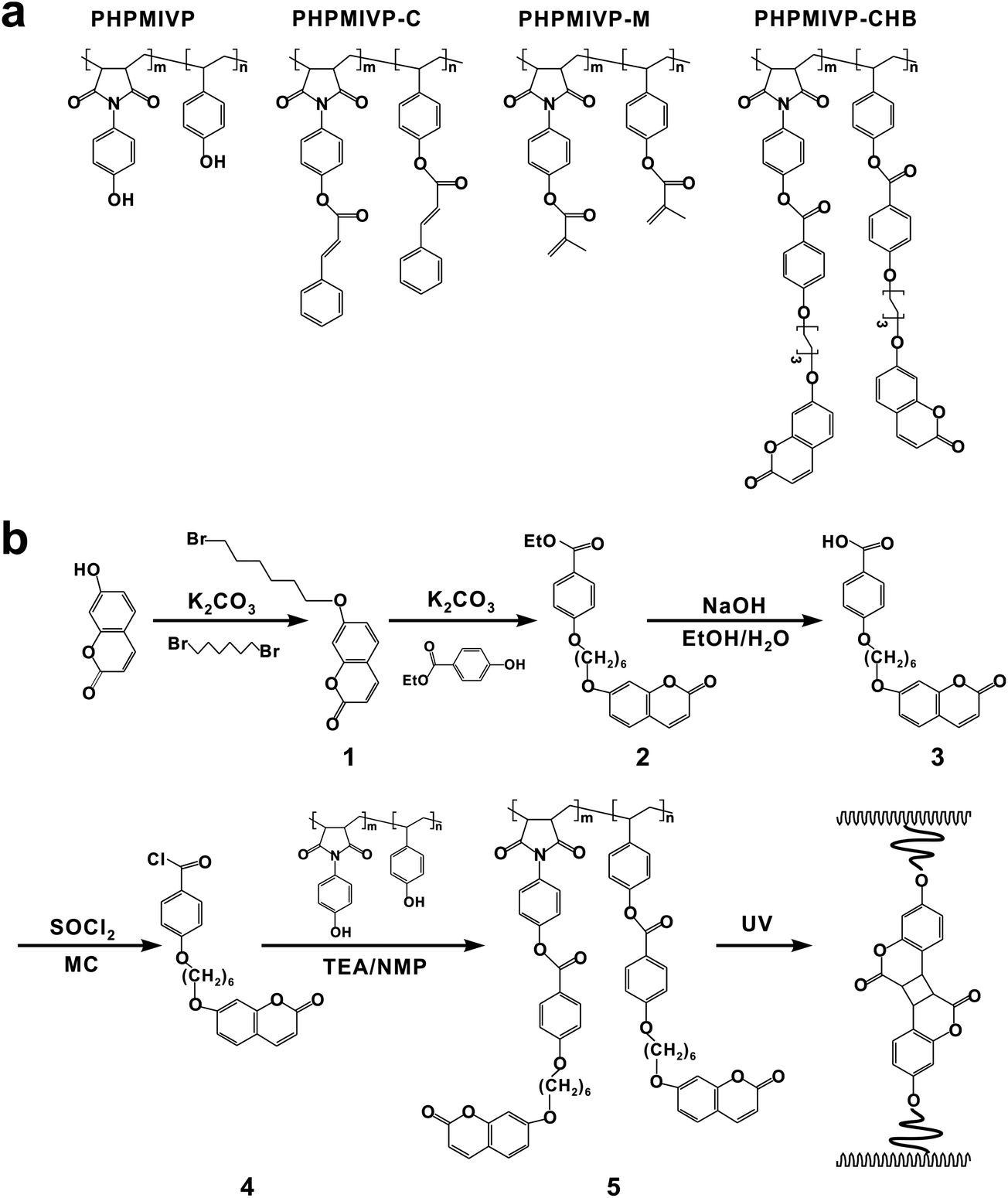 | ||
| Fig. 1 (a) Chemical structures of PHPMIVP derivatives. (b) Synthetic scheme of PHPMIVP-CHB. | ||
Results and discussion
PHPMIVP was synthesized by copolymerizion of 4-acetoxymaleimide and 4-acetoxystyrene, followed by deprotection of acetoxy groups. The reaction feed ratio of 4-acetoxymaleimide and 4-acetoxystyrene was 1 to 1. The molecular weight of PHPMIVP was Mn = 28![[thin space (1/6-em)]](https://www.rsc.org/images/entities/char_2009.gif) 000 g mol−1 (PDI = 2.33). Photo-curable polymers were synthesized by reacting PHPMIVP with cinnamoyl chloride (PHPMIVP-C) (Mn = 51000 g mol−1), methacroyl chloride (PHPMIVP-M) (Mn = 40000 g mol−1) or 4-(6-(7-coumarinyloxyl)hexyloxy)benzoyl chloride (PHPMIVP-CHB) (Mn = 92000 g mol−1). The detail synthetic scheme of PHPMIVP-CHB is depicted in Fig. 1b. Due to the high reactivity of acyl chloride with phenol,28 modification of PHPMIVP with each photo-reactive side groups was almost stoichiometric. Because of poor solubility of PHPMIVP derivatives in conventional GPC solvents, their molecular weights were calculated by using the molecular weight of PHPMIVP and the reaction conversions of side-group modifications. The synthesized polymers exhibited high thermal stability. For example, the weight loss of PHPMIVP-CHB at 300 °C was less than 3 wt%. The glass transition temperature (Tg) of PHPMIVP-CHB was 167 °C. The chemical stability of the polymer films was investigated by measuring the leakage current as a function of applied electric field before and after solvent treatment. Furthermore, their surface morphologies were investigated on AFM. For the measurements of the leakage current, metal-insulator-metal (MIM) devices for each polymers were fabricated. Polymer films were first spin-casted on Mo-coated glass substrates from 10 wt% of solutions in cyclohexanon. The thickness was controlled to 500 ± 10 nm. After annealing at 70 °C for 2 min, the films were cured by irradiating UV using a high pressure mercury lamp for 50 s. Prior to coat top electrodes, the films were immersed in various solvents for 1 min including acetone, tetrahydrofuran (THF), 1,2,3,4-tetrahydronaphthalene (tetraline), chloroform and chlorobenzene. After solvent treatment, the films were completely dried on a hot plate at 70 °C for 5 min, and then the top electrodes were formed by evaporating gold on to the polymer films. For comparison, MIM devices using thermally crosslinked PVP which is one of the most common polymers for high performance gate dielectrics were also prepared similarly. As shown in Fig. 2, each polymer shows quite different electrical response to the applied electric voltage. While uncrosslinked PHPMIVP and thermally crosslinked PVP exhibited high leakage current and low breakdown voltage, photo-cured polymers showed much enhanced electrical properties. Especially, PHPMIVP-CHB showed significantly low leakage current which is almost 5 orders lower than that of thermally cured PVP at 1 MV cm−1 of the applied electric field, and no observable breakdown voltage at least up to 4 MV cm−1. It is notable that the dielectric constant of PHPMIVP-CHB (εr = 3.86) is higher than that of PVP (εr = 3.60) (Table 1). This implies that the low leakage current and high breakdown voltage is not benefited by dielectric constant of polymer. We attribute the lowered leakage current and the elevated breakdown voltage to the high crosslinking density of PHPMIVP-CHB. Since the reduced the free volume by crosslinking increases the energy compensation for ionization, electron tunnelling can be impeded by increasing the extent of crosslinking.29,30
000 g mol−1 (PDI = 2.33). Photo-curable polymers were synthesized by reacting PHPMIVP with cinnamoyl chloride (PHPMIVP-C) (Mn = 51000 g mol−1), methacroyl chloride (PHPMIVP-M) (Mn = 40000 g mol−1) or 4-(6-(7-coumarinyloxyl)hexyloxy)benzoyl chloride (PHPMIVP-CHB) (Mn = 92000 g mol−1). The detail synthetic scheme of PHPMIVP-CHB is depicted in Fig. 1b. Due to the high reactivity of acyl chloride with phenol,28 modification of PHPMIVP with each photo-reactive side groups was almost stoichiometric. Because of poor solubility of PHPMIVP derivatives in conventional GPC solvents, their molecular weights were calculated by using the molecular weight of PHPMIVP and the reaction conversions of side-group modifications. The synthesized polymers exhibited high thermal stability. For example, the weight loss of PHPMIVP-CHB at 300 °C was less than 3 wt%. The glass transition temperature (Tg) of PHPMIVP-CHB was 167 °C. The chemical stability of the polymer films was investigated by measuring the leakage current as a function of applied electric field before and after solvent treatment. Furthermore, their surface morphologies were investigated on AFM. For the measurements of the leakage current, metal-insulator-metal (MIM) devices for each polymers were fabricated. Polymer films were first spin-casted on Mo-coated glass substrates from 10 wt% of solutions in cyclohexanon. The thickness was controlled to 500 ± 10 nm. After annealing at 70 °C for 2 min, the films were cured by irradiating UV using a high pressure mercury lamp for 50 s. Prior to coat top electrodes, the films were immersed in various solvents for 1 min including acetone, tetrahydrofuran (THF), 1,2,3,4-tetrahydronaphthalene (tetraline), chloroform and chlorobenzene. After solvent treatment, the films were completely dried on a hot plate at 70 °C for 5 min, and then the top electrodes were formed by evaporating gold on to the polymer films. For comparison, MIM devices using thermally crosslinked PVP which is one of the most common polymers for high performance gate dielectrics were also prepared similarly. As shown in Fig. 2, each polymer shows quite different electrical response to the applied electric voltage. While uncrosslinked PHPMIVP and thermally crosslinked PVP exhibited high leakage current and low breakdown voltage, photo-cured polymers showed much enhanced electrical properties. Especially, PHPMIVP-CHB showed significantly low leakage current which is almost 5 orders lower than that of thermally cured PVP at 1 MV cm−1 of the applied electric field, and no observable breakdown voltage at least up to 4 MV cm−1. It is notable that the dielectric constant of PHPMIVP-CHB (εr = 3.86) is higher than that of PVP (εr = 3.60) (Table 1). This implies that the low leakage current and high breakdown voltage is not benefited by dielectric constant of polymer. We attribute the lowered leakage current and the elevated breakdown voltage to the high crosslinking density of PHPMIVP-CHB. Since the reduced the free volume by crosslinking increases the energy compensation for ionization, electron tunnelling can be impeded by increasing the extent of crosslinking.29,30
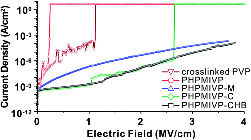 | ||
| Fig. 2 The changes of leakage current density as a function of electric field for various polymer films. | ||
Solvent treatment significantly altered the electrical properties of the films. The changes of leakage current density were measured for the polymer films of PVP, PHPMIVP-M and PHPMIVP-CHB after treating with various solvents (Fig. 3). As shown in Fig. 3a, leakage current density of PVP film sharply increased after treating with solvents. As increasing electric field, all films treated with solvents including acetone, THF, tetraline, chloroform and chlorobenzene showed fast increase of leakage current density, and the leakage current density became saturated to ∼10−2 A cm−2 before the electric field increased to 0.5 MV cm−1. AFM analysis revealed that the abrupt increase of leakage current is mainly due to the formation of many pinholes after solvent treatment. As shown in Fig. 4, the as-prepared PVP film originally formed uniform and clean surface. However, many pinholes were observed on the film surfaces after solvent treatment although the film thickness didn't changed by solvent treatment. We attribute that that pinholes were formed by partial swelling and deswelling by solvents. Photo-curable PHPMIVP-M showed better solvent resistance than PVP (Fig. 3b). The leakage current density of PHPMIVP-M film didn't change much without showing breakdown below 4 MV cm−1 after treating with solvents having moderate solvation power such as acetone and THF. PHPMIVP-M films, however, were damaged for the solvents having stronger solvation power including chloroform, tetraline and chlorobenzene. The breakdown voltages were observed at 3.5 MV cm−1, 2.2 MV cm−1 and 0.9 MV cm−1 when the film was treated with chloroform, tetraline and chlorobenzene respectively. PHPMIVP-CHB films exhibited very high solvent resistance. The leakage current density curves were almost identical with that of as-prepared film after treating with all given solvents. AFM micrographs showed that PHPMIVP-CHB films were barely influenced by solvent treatment (Fig. 5). Unlike PVP films shown in Fig. 4, no pinhole was observed on PHPMIVP-CHB films after solvent treatments. The root mean square (RMS) roughness and the dielectric constant were barely changed by solvent treatments (Table 2). These results imply that PHPMIVP-CHB films are not swollen by given solvent set. Besides above mentioned solvents, PHPMIVP-CHB films also exhibited strong chemical resistance to photoresist stripper (PRS2000) and Au etchant (KI solution) which can be exposed to during the practical manufacturing processes.
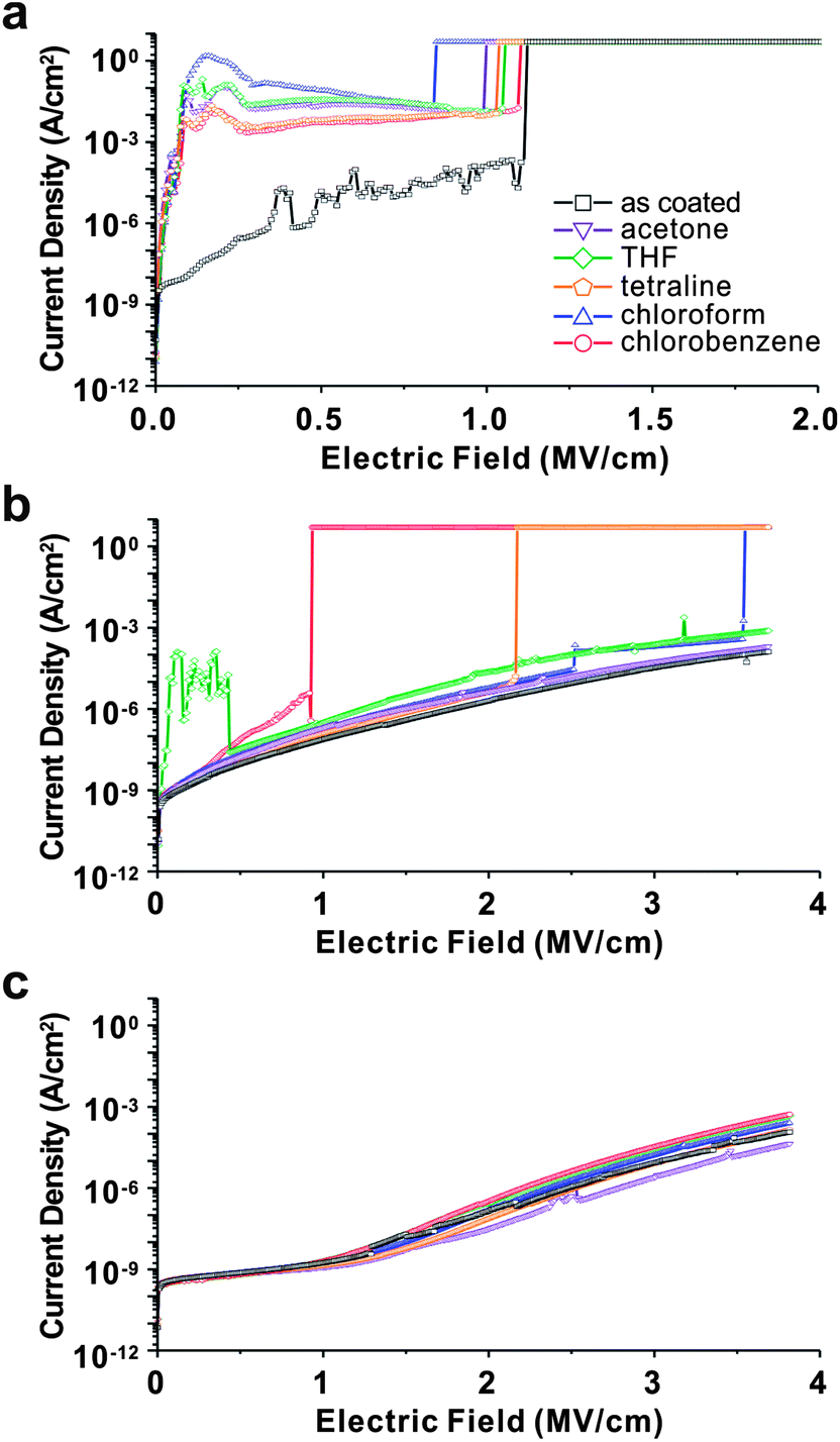 | ||
| Fig. 3 The changes of leakage current density as a function of electric field for the polymer films after treating with solvents including acetone, THF, tetraline, chloroform and chlorobenzene; (a) thermally cured PVP, (b) photo-crosslinked PHPMIVP-M and (c) photo-crosslinked PHPMIVP-CHB. | ||
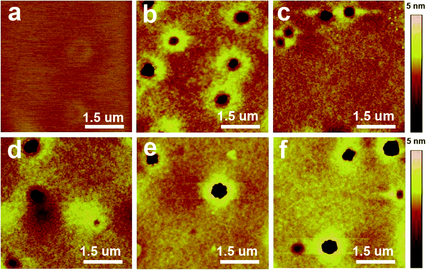 | ||
| Fig. 4 The effects of solvent treatment on the morphology of the crosslinked PVP films. The films formed on silicon wafers with a thickness of 100 nm by spin-casting from a solution of PVP/poly(melamine-co-formaldehyde) in cyclohexanon (10 wt%), and thermally cured at 200 °C for 2 hours. AFM micrographs of (a) the as-prepared film, and taken after immersing the films in (b) acetone, (c) THF, (d) tetraline, (e) chloroform and (f) chlorobenzene for 1 minute. | ||
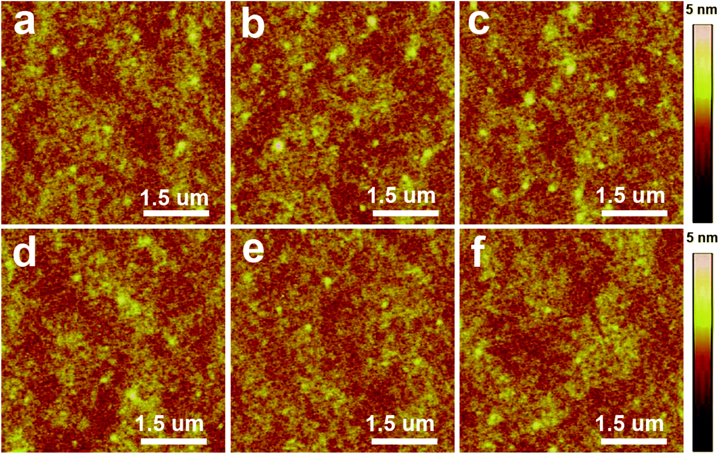 | ||
| Fig. 5 (a–f) The effects of solvent treatment on the morphology of the photo-crosslinked PHPMIVP-CHB films. AFM micrographs of (a) the as-prepared film, and taken after immersing the films in (b) acetone, (c) THF, (d) tetraline, (e) chloroform and (f) chlorobenzene for 1 minute. | ||
| Solvent | Dielectric constant (εr) | RMS roughness |
|---|---|---|
| No solvent treatment | 3.86 | 3.2 Å |
| Acetone | 3.88 | 3.5 Å |
| THF | 3.85 | 3.3 Å |
| Tetraline | 3.83 | 3.3 Å |
| Chloroform | 3.82 | 2.9 Å |
| Chlorobenzene | 3.85 | 3.2 Å |
Utilizing the high solvent resistance, polymer FET devices were fabricated by sequential spin-casting process of polymer gate dielectric layer and polymer semiconducting layer. PQTBTz-C12 which was synthesized by Samsung Advanced Institute of Technology (Mn = 18000 g mol−1) has been used as a polymeric semiconductor in our experiments.31,32 Briefly, PHPMIVP-CHB film was first formed on a highly doped n-type silicon wafer (resistivity < 0.004 Ω cm) with a thickness of 500 nm following the previously described procedures. After photo-curing, PQTBTz-C12 was spin-casted on the PHPMIVP-CHB layer from a 1 wt% solution in chlorobenzene. Finally, the gold source/drain electrodes were formed on the film by using conventional vacuum deposition technique. The channel width and length was 1000 μm and 100 μm respectively. For comparison, other PQTBTz-C12 FET devices were similarly prepared on PVP, PHPMIVP, PHPMIVP-M and PHPMIVP-C gate dielectric films. As shown in Fig. 6, the device performance was highly dependent on polymer gate dielectrics for the same PQTBTz-C12 semiconductor. The highest mobility was measured when the PHPMIVP-CHB dielectric layer was used (μFET = 0.029 cm2 V−1 s−1). The measured mobility for PVP, PHPMIVP, PHPMIVP-C and PHPMIVP-M was μFET = 0.017 cm2 V−1 s−1, μFET = 0.0029 cm2 V−1 s−1, μFET = 0.0016 cm2 V−1 s−1 and μFET = 0.0041 cm2 V−1 s−1 respectively. It is know that the mobility of OFET devices are affected by the charge trapped the interface between the semiconductor and the dielectric as well as interface uniformity. We attribute the decreased mobility for PVP, PHPMIVP, PHPMIVP-M and PHPMIVP-C dielectric films partially to the deterioration of dielectric layer by solvent during the spin-casting of PQTBTz-C12, and partially to the presence of residual hydroxyl groups which may act as the charge trap sites. As demonstrated in Fig. 2 and 3, PHPMIVP, PHPMIVP-M and PHPMIVP-C dielectric films are not sufficiently stable against to chlorobenzene which was used as a solvent for dissolving PQTBTz-C12. Besides benefit in mobility, PHPMIVP-CHB showed hysteresis-free response to the voltage swift, while PHPMIVP and PHPMIVP-M showed strong hysteresis. The threshold voltage and the on/off ratio were 7.4 V and 106 respectively. All these results represent that PHPMIVP-CHB forms chemically and electrically stable dielectric layer which can be applicable for fabricating OTFTs by sequential spin-casting of insulating and semiconducting layers without hampering the electrical properties.
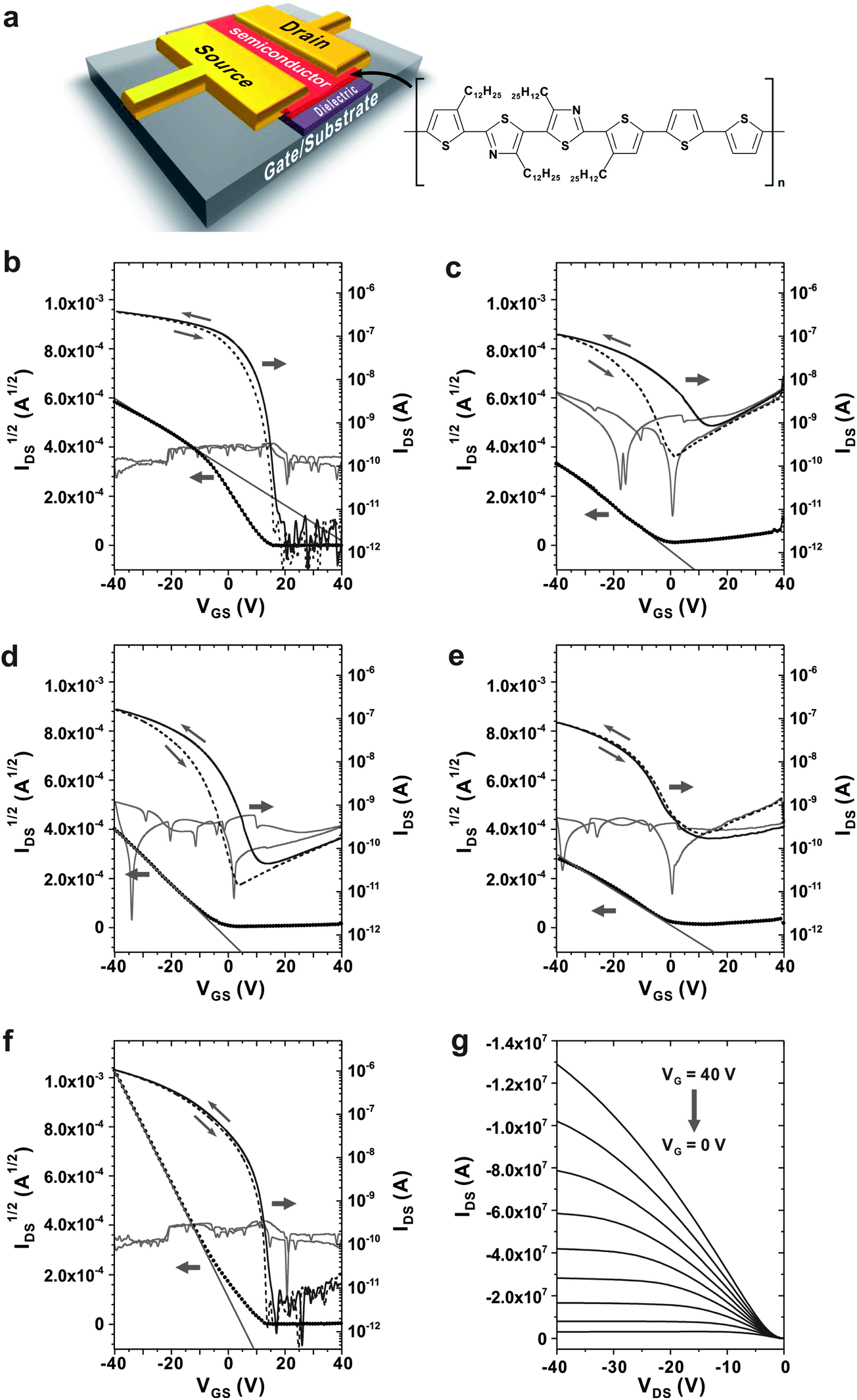 | ||
| Fig. 6 (a) The chemical structure of PQTBTz-C12 and the schematic structure PQTBTz-C12 FET. Transfer characteristics of PQTBTz-C12 FET fabricated on (b) PVP dielectric, (c) PHPMIVP dielectric, (d) PHPMIVP-M dielectric, (e) PHPMIVP-C dielectric and (f) PHPMIVP-CHB dielectric. (g) Output characteristics of PQTBTz-C12 FET fabricated on PHPMIVP-CHB dielectric. | ||
Conclusions
In summary, we have developed the photo-curable polymers for gate dielectric exhibiting high chemical resistance to various solvents and hysteresis-free operations in OTFT devices. The newly developed gate dielectrics are derivatives of PHPMIVP containing photo-reactive side groups such as cinnamoyl chloride, methacroyl chloride or 4-(6-(7-coumarinyloxyl)hexyloxy)benzoyl chloride. PHPMIVP-CHB exhibited high thermal stability and very strong chemical resistance to various organic solvents including acetone, THF, tetraline, chloroform and chlorobenzene, which allow forming dielectric layers and semiconducting layers by sequential spin-casting processes without deterioration of device performance. PHPMIVP-CHB showed consistent responses in the leakage current density curve after treating the films with various solvents without showing breakdown voltage or current density shifts. The field-effect transistors consisting of PHPMIVP-CHB insulating layer and PQTBTz-C12 semiconducting layer were fabricated by sequential spin-casting method. When PHPMIVP-CHB was used for the gate dielectric layer, the transistor showed much better mobility than other polymers with no hysteresis. The mobility was measured at μFET = 0.029 cm2 V−1 s−1 with on/off ratio = 106.Experimental
Materials and methods
All reagents were purchased from Sigma Aldrich and used without further purification. Polymeric semiconductor, PQTBTz-C12 (Mn = 18000 g mol−1) was synthesized following the previously reported procedures.331H-NMR spectra were recorded on DPX Bruker 300 (300 MHz) and Bruker Advance III (600 MHz) spectrometers. Differential scanning calorimetry (DSC) was performed on a DSC Q2000 (TA Instrument) at a heating and cooling rate of 1 °C min−1. Atomic Force Microscope (Digital Instruments Multimode) operating in tapping mode with a silicon cantilever was used to characterize the surface morphologies of the samples.
Synthesis of 6-(7-coumarinyloxyl)hexylbromide (1)
7-Hydroxycoumarin (50 g, 0.308 mol) was first dissolved in 1000 mL of acetone, and then potassium carbonate (85.13 g, 0.616 mol) and 1,6-dibromohexane (150.3 g, 0.616 mol) were added thereto. The mixture was refluxed for 24 hours, and then the reaction mixture was filtered and dried. The obtained filtrate was mixed with ether and water, and then extracted with ether. Finally, the resulting compound was recrystallized in hexane giving the yellow solid (64.89 g, 65% yield).1H NMR (300 MHz, CDCl3, δ): 7.63 (d, J = 9.3 Hz, 1H, aryl H), 7.36 (d, J = 8.7 Hz, 1H, aryl H), 6.82 (m, 2H, aryl H), 6.25 (d, J = 9.3 Hz, 1H, aryl H), 4.03 (t, 2H, aliphatic H), 3.43 (t, 2H, aliphatic H), 1.87 (m, 4H, aliphatic H), 1.53 (m, 4H, aliphatic H).
Synthesis of ethyl 4-(6-(7-coumarinyloxyl)hexyloxy)benzoate (2)
The compound 1 (48.78 g, 0.15 mol) was dissolved in 750 mL of acetone. Potassium carbonate (62 g, 0.75 mol) and ethyl-4-hydroxybenzoate (24.93 g, 0.15 mol) were added thereto and the mixture was refluxed for 24 hours. The reaction mixture was filtered and the filtrate was washed with chloroform and dried. The resulting compound was recrystallized in ethanol giving the light yellow solid (53.74 g, 87.3% yield).1H NMR (300 MHz, CDCl3, δ): 7.98 (d, J = 9 Hz, 1H, aryl H), 7.63 (d, J = 9.6 Hz, 1H, aryl H), 7.36 (d, J = 8.7 Hz, 1H, aryl H), 6.9 (m, J = 9 Hz, 5H, aryl H), 6.24 (d, J = 9.3 Hz, 1H, aryl H), 4.33 (t, J = 7.2 Hz, 2H, aliphatic H), 4.03 (t, J = 6.3 Hz, 2H, aliphatic H), 1.85 (m, 4H, aliphatic H), 1.57 (m, 2H, aliphatic H), 1.37 (m, 2H, aliphatic H).
Synthesis of 4-(6-(7-coumarinyloxyl)hexyloxy)benzoic acid (3)
The compound 2 (53.74 g, 0.13 mol) was dissolved in 600 mL of ethanol. After adding 600 mL of 1 M NaOH solution to the solution, the mixture was stirred for about 48 hours. The reaction mixture was, then, acidified by adding 10% HCl solution and filtered to separate solid. The isolated solid was recrystallized in ethanol giving the light yellow solid (40 g, 80% yield).1H NMR (300 MHz, CDCl3, δ): 7.97 (d, J = 9.6 Hz, 1H, aryl H), 7.85 (m, 2H, aryl H), 7.60 (d, J = 8.4 Hz, 1H, aryl H), 6.96 (m, J = 9 Hz, 4H, aryl H), 6.27 (d, J = 9.6 Hz, 1H, aryl H), 4.05 (m, 4H, aliphatic H), 1.74 (m, 4H, aliphatic H), 1.47 (m, 4H, aliphatic H).
Synthesis of 4-(6-(7-coumarinyloxyl)hexyloxy)benzoyl chloride (CHB) (4)
The compound 3 (5 g, 13.075 mmol) was added to 100 mL of methylene chloride under nitrogen atmosphere, thionyl chlroride (1.71 g, 14.383 mmol) was added thereto and the mixture was stirred at 35 °C for 5 hours. The reaction mixture was dried and used next step as it is.Synthesis of PHPMIVP-CHB (5)
Poly(N-(4-hydroxyphenyl)maleimide-co-4-vinylphenol) (PHPMIVP) (1.685 g, Mn = 28000 g mol−1, PDI = 2.33) was dissolved in 20 mL of THF under nitrogen atmosphere and then cooled down to 0 °C. Next, triethyl amine (1.985 g, 19.61 mmol) was added to the mixture and stirred for 1 hour. The synthesized compound 4 was added to the resulting mixture at 0 °C, and gently heated to the room temperature. The mixture was stirred for 24 hours, and then the reaction mixture was poured into a mixture of methanol/water, to thereby precipitate solid. The solid were isolated by filtration. Finally the filtrate was purified by soxhlet-extraction using methanol as a solvent. The white polymeric solid was finally obtained (6 g).
Metal-insulator-metal (MIM) device fabrication
Capacitance and leakage current of polymer films were measured by using metal-insulator-metal (MIM) type capacitor. Polymer films were first spin-casted on Mo-coated glass substrates from 10 wt% of solutions in cyclohexanon. The thickness was controlled to 500 ± 10 nm. After annealing at 70 °C for 2 min, the films were cured by irradiating UV using a high pressure mercury lamp for 50 s. Prior to coat top electrode, the films were immersed in various solvents for 1 min including acetone, tetrahydrofuran (THF), 1,2,3,4-tetrahydronaphthalene (tetraline), chloroform and chlorobenzene. After solvent treatment, the films were completely dried on a hot plate at 70 °C for 5 min, and then the top electrode was formed by evaporating gold on to the polymer films.Preparation and characterization of OTFT
The electrical properties of PQTBTz-C12 were characterized by using OTFT with top-contact geometry. For the fabrication of PQTBTz-C12 FET, PHPMIVP-CHB film was first formed on a highly doped n-type silicon wafer (resistivity < 0.004 Ω cm) with a thickness of 500 nm. After photo-curing the PHPMIVP-CHB film, PQTBTz-C12 was spun on the PHPMIVP-CHB layer from a 1 wt% solution in chlorobenzene. Finally, the gold source/drain electrodes were formed on the film by using conventional vacuum deposition technique. The channel width and length was 1000 μm and 100 μm respectively. Current transfer characteristic curves of the prepared OTFT devices were obtained in a saturation regime (VSD = −40 V) by using a semiconductor characterization system 4200-SCS (Keithley Instrument).Acknowledgements
This work was supported by the National Research Foundation of Korea (NRF) grant funded by the Korea government (2011–0017197), NRF (2012M2A2A6035933) and by Basic Science Research Program through the National Research Foundation of Korea (NRF) funded by the Ministry of Education (2012R1A6A1029029).References
- Z. Bao, Nat. Mater., 2004, 3, 137–138 CrossRef CAS PubMed.
- H. E. Katz and J. Huang, Annu. Rev. Mater. Res., 2009, 39, 71–92 CrossRef CAS.
- A. Facchetti, M.-H. Yoon and T. J. Marks, Adv. Mater., 2005, 17, 1705–1725 CrossRef CAS.
- R. A. Street, W. Wong, S. Ready, M. Chabinyc, A. Arias, S. Limb, A. Salleo and R. Lujan, Mater. Today, 2006, 9, 32–37 CrossRef CAS.
- S. Nelson, Y.-Y. Lin, D. Gundlach and T. Jackson, Appl. Phys. Lett., 1998, 72, 1854–1856 CrossRef CAS.
- H. Klauk, M. Halik, U. Zschieschang, G. Schmid, W. Radlik and W. Weber, J. Appl. Phys., 2002, 92, 5259–5263 CrossRef CAS.
- H. S. Lee, K. Park, J.-D. Kim, T. Han, K. H. Ryu, H. S. Lim, D. R. Lee, Y.-J. Kwark and J. H. Cho, J. Mater. Chem., 2011, 21, 6968–6974 RSC.
- J. Jang, S. Nam, J. Hwang, J.-J. Park, J. Im, C. E. Park and J. M. Kim, J. Mater. Chem., 2012, 22, 1054–1060 RSC.
- G. Gu, M. G. Kane, J. E. Doty and A. H. Firester, Appl. Phys. Lett., 2005, 87, 243512 CrossRef.
- H. E. Katz, X. M. Hong, A. Dodabalapur and R. Sarpeshkar, J. Appl. Phys., 2002, 91, 1572–1576 CrossRef CAS.
- T. B. Singh, N. Marjanovic, P. Stadler, M. Auinger, G. Matt, S. Gunes, N. Sariciftci, R. Schwodiauer and S. Bauer, J. Appl. Phys., 2005, 97, 083714 CrossRef.
- C. Kim, A. Facchetti and T. J. Marks, Science, 2007, 318, 76–80 CrossRef CAS PubMed.
- P. O. Jackson, M. O'Neill, W. L. Duffy, P. Hindmarsh, S. M. Kelly and G. J. Owen, Chem. Mater., 2001, 13, 694–703 CrossRef CAS.
- C. Kim, Z. Wang, H.-J. Choi, Y.-G. Ha, A. Facchetti and T. J. Marks, J. Am. Chem. Soc., 2008, 130, 6867–6878 CrossRef CAS PubMed.
- L. Kaake, Y. Zou, M. Panzer, C. Frisbie and X.-Y. Zhu, J. Am. Chem. Soc., 2007, 129, 7824–7830 CrossRef CAS PubMed.
- S. Y. Yang, K. Shin and C. E. Park, Adv. Funct. Mater., 2005, 15, 1806–1814 CrossRef CAS.
- T. Ahn, J. W. Kim, Y. Choi and M. H. Yi, Org. Electron., 2008, 9, 711–720 CrossRef CAS PubMed.
- S. Pyo, M. Lee, J. Jeon, J. H. Lee, M. H. Yi and J. S. Kim, Adv. Funct. Mater., 2005, 15, 619–626 CrossRef CAS.
- J. Puigdollers, C. Voz, A. Orpella, R. Quidant, I. Martın, M. Vetter and R. Alcubilla, Org. Electron., 2004, 5, 67–71 CrossRef CAS PubMed.
- L.-L. Chua, P. K. Ho, H. Sirringhaus and R. H. Friend, Appl. Phys. Lett., 2004, 84, 3400–3402 CrossRef CAS.
- J. Ghim, K.-J. Baeg, Y.-Y. Noh, S.-J. Kang, J. Jo, D.-Y. Kim, S. Cho, J. Yuen, K. Lee and A. J. Heeger, Appl. Phys. Lett., 2006, 89, 202516 CrossRef.
- J. Li, Z. Sun and F. Yan, Adv. Mater., 2012, 24, 88–93 CrossRef CAS PubMed.
- J. Jang, S. H. Kim, S. Nam, D. S. Chung, C. Yang, W. M. Yun, C. E. Park and J. B. Koo, Appl. Phys. Lett., 2008, 92, 143306 CrossRef.
- M.-H. Yoon, H. Yan, A. Facchetti and T. J. Marks, J. Am. Chem. Soc., 2005, 127, 10388–10395 CrossRef CAS PubMed.
- D.-W. Park, C. A. Lee, K.-D. Jung, B.-G. Park, H. Shin and J. D. Lee, Appl. Phys. Lett., 2006, 89, 263507 CrossRef.
- M. E. Roberts, N. r. Queraltó, S. C. Mannsfeld, B. N. Reinecke, W. Knoll and Z. Bao, Chem. Mater., 2009, 21, 2292–2299 CrossRef CAS.
- R. H. Huyck, S. R. Trenor, B. J. Love and T. E. Long, J. Macromol. Sci., Part A: Pure Appl.Chem., 2007, 45, 9–15 CrossRef.
- M. B. Smith and J. March, March's advanced organic chemistry: reactions, mechanisms, and structure, John Wiley & Sons, Inc., United States of America, 2007 Search PubMed.
- S. H. Kim, S. Y. Yang, K. Shin, H. Jeon, J. W. Lee, K. P. Hong and C. E. Park, Appl. Phys. Lett., 2006, 89, 183516 CrossRef.
- V. Zakrevskii, N. Sudar, A. Zaopo and Y. A. Dubitsky, J. Appl. Phys., 2003, 93, 2135–2139 CrossRef CAS.
- D. H. Kim, B.-L. Lee, H. Moon, H. M. Kang, E. J. Jeong, J.-I. Park, K.-M. Han, S. Lee, B. W. Yoo and B. W. Koo, J. Am. Chem. Soc., 2009, 131, 6124–6132 CrossRef CAS PubMed.
- B.-L. Lee, K.-M. Han, E.-K. Lee, I.-N. Kang, D. H. Kim and S. Lee, Synth. Met., 2009, 159, 132–136 CrossRef CAS PubMed.
- S.-J. Choi, J.-H. Kim and H. H. Lee, IEEE Electron Device Lett., 2009, 30, 454–456 CrossRef CAS.
| This journal is © The Royal Society of Chemistry 2014 |