ZnO(N)–Spiro-MeOTAD hybrid photodiode: an efficient self-powered fast-response UV (visible) photosensor†
Onkar
Game
*abc,
Upendra
Singh
ab,
Tanya
Kumari
ab,
Arun
Banpurkar
c and
Satishchandra
Ogale
*ab
aCentre for Excellence in Solar Energy, Physical and Materials Chemistry Division, National Chemical Laboratory (CSIR-NCL), Pune 411 008, India
bNetwork Institute of Solar Energy (CSIR-NISE), New Delhi, India. E-mail: sb.ogale@ncl.res.in; satishogale@gmail.com; Fax: +91 20 2590 2636
cDepartment of Physics, University of Pune, Ganeshkhind, Pune-411 007, India. E-mail: onkar.game@gmail.com
First published on 14th October 2013
Abstract
Organic–inorganic hybrid photo-detectors with a self-sufficient mode of operation represent a research area of great current interest. In most efficient photodetectors and optoelectronic devices compound semiconductors containing toxic elements such as Cd, As, Te, S, Se etc. are used and these are also expensive. Hence there is also a rapidly growing interest in replacing these with environmentally friendly and earth-abundant materials. Herein, we report a facile solution-processed fabrication of a self-powered organic–inorganic hybrid photodetector using n-type oriented ZnO nanorods and p-type Spiro-MeOTAD semiconductor. ZnO is eco-friendly and earth-abundant, and Spiro-MeOTAD is non-hazardous. We show that the latter has far less toxicity than the toxic elements stated above. This visible blind UV photodetector shows high sensitivity (102) and a UV/visible rejection ratio of 300. It also exhibits fast response times of τrise ∼ 200 μs and τfall ∼ 950 μs. Importantly, with a small modification of nitrogen incorporation in ZnO one can also realize a highly-sensitive self-powered visible light photodetector with at least 1000% (or higher) improvements in quality factors (photocurrent/sensitivity/response time) as compared to previously reported organic–inorganic hybrid photo-detectors based on metal-chalcogenides (CdS–PANI or CuInSe2–P3HT). Interestingly, the broadband sensitivity of such N:ZnO–Spiro-MeOTAD photodiode enables sensing of low intensity (∼28 μW cm−2) ambient white light with a high photocurrent density of 120 nA cm−2 making it an efficient ambient white light detector.
Introduction
Photodetectors with response in the UV and/or visible region are used in a wide range of applications from everyday consumer electronics (compact disc players, smoke detectors, remote control) to more sophisticated applications such as environmental monitoring, space research and optical communication.1,2 Photodetectors operate on various principles such as photo-electrochemistry3 photoconduction or photodiode action.4 In order to get reasonable detectivity, most of the photodetectors need a certain applied potential (1–100 V) which therefore requires a constant use of batteries (power). This makes the overall circuitry heavy and uneconomical in the current energy scenario. The ‘self-powered’ photo-detectors which are either integrated with an energy harvesting unit such as biofuel cell or pizotronic circuitry,5 or which can generate self-sufficient potential for their operation6 have lately attracted considerable attention from scientists and technologists.Photodiodes (Schottky or p–n junction type) operated in a photovoltaic short-circuit or open-circuit modes form an important class of such self-powered photodetectors.6,7 Most such photo-diodes employ nanostructured inorganic semiconductors8–10 which exhibit attractive functionalities such as high carrier mobility and high absorption coefficients; but they suffer from drawbacks such as high temperature (>800 °C) synthesis, complex device fabrication methods and low flexibility. On the other hand organic semiconductors are solution processable, with good flexibility and functional tunability through modifications of involved monomers/molecules; but they suffer from relatively low carrier mobility values. Therefore, hybrid organic–inorganic semiconductor junctions are envisaged to complement each others' functional advantages while overcoming their respective drawbacks.
There is an impressive body of work reported in the literature on organic–inorganic hybrid photodetectors11–16 with good response both in the UV and/or visible region(s). However most of these hybrid photo-detectors employ compounds of rare elements such as indium (In), gallium (Ga) germanium (Ge) or toxic elements such as cadmium (Cd), sulfur (S), selenium (Se) etc., thereby raising a concern over the possible health and environmental hazards when produced on an industrial scale. Recently, there have been a few interesting reports17 on hybrid visible light photo-detectors using earth abundant or nontoxic elements, but these lack the self-powered mode of operation. Therefore, organic–inorganic hybrid photo-detectors involving use of non-toxic components and operating under self-sufficient power mode are highly desired.
Zinc oxide (ZnO) is an environmentally friendly, non-toxic metal–oxide semiconductor with a wide range of optoelectronic applications due to its several attractive physical properties.18 In particular, this is an n-type semiconductor with very high carrier mobility (>100 cm2 V−1 s−1 at RT, >2000 cm2 V−1 s−1 at 80 K) and crystal habits that allow growth of diverse nanostructured morphologies. Among the various morphologies of ZnO, quasi one dimensional (quasi-1D) nanorods are particularly interesting because their single crystalline nature offers efficient carrier transport and higher diffusion length. Low temperature (∼90 °C) solution synthesis of single crystalline ZnO nanorod arrays on conducting substrates makes ZnO the most preferred candidate for hybrid devices over many other semiconductors used in photodetectors that require high temperature (>800 °C) physical vapor deposition synthesis.15
Among various p-type organic semiconductors 2,2′,7,7′-tetrakis (N,N-di-p-methoxyphenylamine)9,9′-spirobifluorene (Spiro-MeOTAD) is an attractive hole-conductor which is widely used in optoelectronic applications such as solid-state dye sensitized solar cells (DSSCs)19 or light emitting diodes.20 Efficient hole regeneration capability and high pore-filling fraction within mesoporous nanostructured films make Spiro-MeOTAD a preferred hole-conductor over other high-conductivity polymers such as poly-3-hexylthiophene-2,5-diyl (P3HT) or solution processable but highly toxic inorganic hole-conductors such as copper thiocyanide (CuSCN).21,22 To our best knowledge, this is the first report where Spiro-MeOTAD is used ias an organic–inorganic hybrid photodetector.
In this report, we first prepared an organic–inorganic hybrid self-powered UV photodiode using p-type Spiro-MeOTAD and solution-processed n-type ZnO nanorods arrays. The UV photodiode showed an impressive UV to visible rejection ratio of 102 and a high photocurrent density/photo-responsivity, at least 250% higher than recently reported all inorganic ZnO-based photodiodes which employ highly toxic components such as CuSCN.23 Equally importantly, the hybrid UV photodetector showed a photo-response (τr ∼ 200 μs and τd ∼ 950 μs) faster than that of previously reported self-powered photo-electrochemical cell (PECC) type photodetectors3 or organic–inorganic hybrid UV photodetectors.24,25 Additionally, with a slight but important modification of in situ N doping in ZnO, we could also obtain a highly-sensitive visible light photodiode with a remarkable set of parameters. Our N:ZnO–Spiro-MeOTAD visible-light hybrid photodetector showed an absorption onset at 650 nm which is further red-shifted in the visible region as compared to absorption onset of common visible light sensitive semiconductors such as cadmium sulfide or zinc indium sulfide. The various parameters of our self-powered N:ZnO–SpiroMeOTAD visible-light photodetector are at least 1000% superior as compared to previously reported ones on ZnO26,27 or metal chalcogenide based organic–inorganic hybrid visible photodetectors such as CuInSe2–P3HT,14 Cu2ZnSnS4–P3HT17 or CdS–PANI.28 Most importantly, we show that N:ZnO–SpiroMeOTAD visible-light photodiode can be used to sense low intensity (28 μW cm−2) of ambient room light with a high photocurrent on/off ratio of 102. To our knowledge, this has not been demonstrated previously. All solution processing, use of non-toxic materials, impressive broadband performance, high sensitivity and fast response are the key highlights of the N:ZnO–SpiroMeOTAD photodetector system demonstrated here.
Experimental
Materials and synthesis
The synthesis of ZnO nanorods on fluorine doped tin oxide (FTO) substrates was performed using a reported protocol29,30 The seed solution was first prepared by dissolving zinc acetate (Sigma Aldrich, 22.8 mM) in ethanol and then drop-cast on a clean substrate followed by heating it for 5 min at 350 °C. This process was repeated twice and then the substrate was annealed for 30 min at 450 °C. For the growth of ZnO nanorods, separate solutions of zinc nitrate hexahydrate (Merck, 25 mM) and hexamethylene tetramine (HMTA) (Sigma Aldrich, 25 mM) were prepared in D.I. water. Polyethylenimine (PEI) (Sigma Aldrich, Mw: 1800, 5 mM) was added to HMTA solution with continuous stirring, followed by addition of this solution to zinc nitrate solution. The seeded substrates were immersed into the growth solution contained in a closed glass container with the seeded side facing the bottom of the glass container. Further, the container was heated to 95 °C on the magnetic heater-cum-stirrer for three hours. After the reaction was complete, the grown ZnO NRs were thoroughly rinsed several times with D.I. water and finally with ethanol, and then dried under IR lamp. The obtained ZnO nanorod films were annealed at 450 °C for 30 min to remove the residual polymer and achieve better adhesion. The final appearance of the films was white in color.The nitrogen doped ZnO (NZnO) nanorod arrays were grown on FTO using similar protocol as described for ZnO nanorod synthesis with some modifications. The growth solution was zinc nitrate (40 mM), HMTA (40 mM) and PEI (5 mM) solutions. In addition to this, ammonia solution (Merck, 25%, 3.8 mL) was added to the growth, which acts as a source of nitrogen. Further, these tightly closed glass vials containing seeded substrates were heated to 100 °C in a silicon oil bath for 30 min. The NZnO nanorod films were annealed at 450 °C for 30 min and the final appearance of the films changed to yellowish-orange due to defects created by nitrogen doping. X-Ray diffraction (XRD) was recorded on a Philips X'Pert PRO using Cu Kα radiation. UV-visible diffused reflectance spectra were recorded using a Jasco V-570 spectrophotometer. The Raman spectra for ZnO samples were obtained using a Horiba Jobin Yvon Lab RAM HR System. The solution of Spiro-OMeTAD was prepared by dissolving Spiro-OMeTAD (68 mM), tert butylpyridine (55 mM) and lithium bis(trifluoromethylsyfonyl)imide salt (9 mM) in chlorobenzene.
Device fabrication and characterization
25 μL of a Spiro-MeOTAD solution was drop cast on ZnO or NZnO nanorod films and spun at a rate of 2000 RPM for 45 s. Ag electrode was thermally evaporated onto ZnO or N:ZnO films as a top contact whereas FTO acted as bottom contact. The electrical characterization was done using Keithly 2420 source meter and Lab Tracer 2.0 software. Blue, green, red and white light LEDs (Luxeon batwing 1 W) were used as visible light sources for different wavelengths. The power of LEDs at different intensities was recorded using Coherent Laser Power Energy Meter, and Lab Max Top-0824C10R Photodiode. TES 1332A Digital Lux-meter was used to measure the intensity of white light. Response time measurements were made using Tetronix MSO 2024 Mixed Signal Oscilloscope.Results and discussion
ZnO–SpiroMeOTAD (ZnO–SPD) UV photodiode
Fig. 1(a) shows the X-ray diffraction (XRD) of ZnO nanorod (NR) arrays grown on FTO. The presence of a sharp (002) peak at 34.4° implies that the nanorods are oriented along the [0001] direction. The inset of Fig. 1(a) shows a characteristic ZnO band edge absorbance at 385 nm in a normalized UV-Vis absorbance spectrum which corresponds to a band gap of 3.2 eV. Fig. 1(b) shows the SEM image of an oriented ZnO NR array on FTO with a length of ∼1 μm and width ∼200 to 300 nm. The tilted (45°) view of Spiro-MeOTAD–ZnO NR p–n junction shows well-percolated hole transport material within the gaps of ZnO nanorods. Good pore-filling of Spiro-MeOTAD within nanostructured ZnO nanorods gives a higher p–n interfacial area resulting in a high rectification ratio and photocurrent density. | ||
| Fig. 1 (a) XRD and UV-Vis absorbance (inset) of a ZnO nanorod film on FTO, (b) SEM of ZnO nanorod arrays with inset showing a 45° tilted view of ZnO NR film infiltrated with Spiro-MeOTAD (c) device schematic and energy level diagram of ZnO–SpiroMeOTAD photodiode, (d) IV curve of ZnO–SPD under dark and UV (390 nm) with intensity 3 mW cm−2, (e) I–V curve in (d) plotted on absolute-semilog scale, (f) photo-response of ZnO–SPD under 3 mW cm−2 UV (390 nm) illumination under alternate on and off cycles. | ||
Fig. 1(c) shows the schematic of ‘ZnO–Spiro-MeOTAD Photodiode’ (ZnO–SPD) and the corresponding energy level diagram. It is clear that higher energy gaps (Eg ≥ 3 eV) and favorable energy alignment of ZnO and Spiro-MeOTAD make them suitable candidates for UV sensing application. The dark J–V curve of ZnO–SPD in Fig. 1(d) shows a typical p–n junction rectifying curve with a low turn-on voltage of 0.2 V and a fairly high rectification ratio (RR) of 2.3 × 10² at a low bias of ±0.5 V. The RR for ZnO–SPD is smaller by one order of magnitude than the recently reported ZnO nanorod based all inorganic photo-diodes.31 The low RR values in organic–inorganic hybrid p–n junctions as compared with their all inorganic counterparts can be assigned to high diode ideality factors in organic–inorganic hybrid systems.12,24 Using the dark IV curve for ZnO–SPD and the diode equation,12,24 the ideality factor for ZnO–SPD was found to be 3.4. A high value of the ideality factor points towards the presence of recombination losses probably due to surface trap states at ZnO–Spiro-MeoTAD interface or a leakage current at Spiro-MeOTAD–FTO interface. Nevertheless, the RR value of 230 is one order of magnitude higher than the previously reported RR values12,23 for ZnO NR based organic–inorganic hybrid photodiodes at a bias of ±0.5 V. This can be attributed to appropriate energy alignment, fairly good pore-filling of SpiroMeOTAD, and a low leakage current at the Spiro-MeOTAD–FTO interface. Therefore, ZnO–SPD heterojunction is a good candidate for low-voltage optoelectronic applications. Fig. 1(d) also shows the J–V curve of ZnO–SPD under low intensity (3 mW cm−2) UV (390 nm) illumination. The photo-response can be seen in both forward and reverse bias conditions. The inset of Fig. 1(d) shows a magnified J–V curve of ZnO–SPD near zero bias which clearly shows a small photovoltaic effect (Voc ∼ 29 mV, Jsc ∼ 50 μA cm−2) in the presence of UV (3 mW cm−2) illumination, and hence points towards the feasibility of using ZnO–SPD under a self-power mode (i.e. at V ∼ 0 V). When ZnO–SPD J–V curves under dark and illumination are plotted on a semilogarithmic scale in Fig. 1(e), a maximum sensitivity (Ilight/Idark) of 3 × 10² is noted at a zero applied bias, reflecting its self-powered mode of operation.
Fig. 1(f) shows the semilogarithmic plot of photocurrent vs. time of unbiased ZnO–SPD under chopped (10 s on and 10 s off) UV light (3 mW cm−2). A clear on/off ratio of 3 × 10² is observed on the semilog scale. The peak photocurrent density is observed to be 50 μA cm−2 at 3 mW cm−2 UV irradiation, which is a factor of two higher than recently reported values for solution-processed ZnO based self-powered UV photodetector.23,32
In order to further investigate the spectral response of ZnO–SPD we calculated wavelength dependant responsivity R(λ) from the external quantum efficiency (EQE) measured using a standard Newport quantum efficiency setup and the expression R(λ) = EQE/hν. Fig. 2 shows the responsivity of ZnO–SPD with maximum responsivity of ∼17 mA W−1 at 390 nm which closely matches the band edge absorption of ZnO and Spiro-MeoTAD. The UV responsivity of 17 mA W−1 at 390 nm is at least a factor of two higher than previously reported self-powered23,32,33 UV photodetectors for 390 nm wavelength.
 | ||
| Fig. 2 Spectral responsivity of ZnO–SPD showing a high UV to visible rejection ratio. | ||
Importantly, the UV to visible rejection ratio is found to be 3 × 10² making it suitable for visible blind UV detection applications.
The response time of photodetectors is another significant parameter for high speed optoelectronic applications. The time resolution (typically 30–40 ms) of the measurement unit can limit the response time of a photodetector. Thus to determine the response times more accurately we used a pulsating source of UV (365 nm) light generated by keeping a mechanical chopper rotating at a frequency of 230 Hz in front of a continuous UV source. An oscilloscope (Tetronix MSO 2024, 200 MHz bandwidth) was used to measure the transient voltage generated across 1 MΩ resistance connected in series with ZnO–SPD.
Fig. 3(a) shows a schematic setup for measurement of the response time. The rise time (τrise) and fall time (τfall) are then defined as the times taken by the signal to vary between 10 and 90% of the saturation value. Fig. 3(b) shows the semilog plot of voltage (caused by photocurrent in ZnO–SPD) vs. time measured across a 1 MΩ resistance. A clear saturation is observed in the transient signal with a rise time of 200 μs and a fall time of 950 μs. The rise and fall times observed here are one order of magnitude faster than previously reported values for ZnO based self-powered organic–inorganic hybrid photo-detectors.3,24,25,27 The faster response time can be attributed to efficient hole regeneration capability of Spiro-MeOTAD due to better pore-filling as compared to other organic semiconductors in hybrid photodiodes. Recently, some reports23,32,34 have also used a nanosecond pulsed UV laser as an alternative to the mechanically chopped UV source for measurement of τrise and τfall. We point out in ESI-1† that although such measurements are useful to get information about charge-transfer dynamics, they may give inappropriate values of the response time. The parameters of self-powered ZnO–SPD reported here are superior to previously reported ones for organic–inorganic hybrid UV photodiodes. Importantly, the materials involved in fabrication of the photodiode reported here are non toxic, and environment friendly in contrast to previous reports on self-powered photodetectors.23
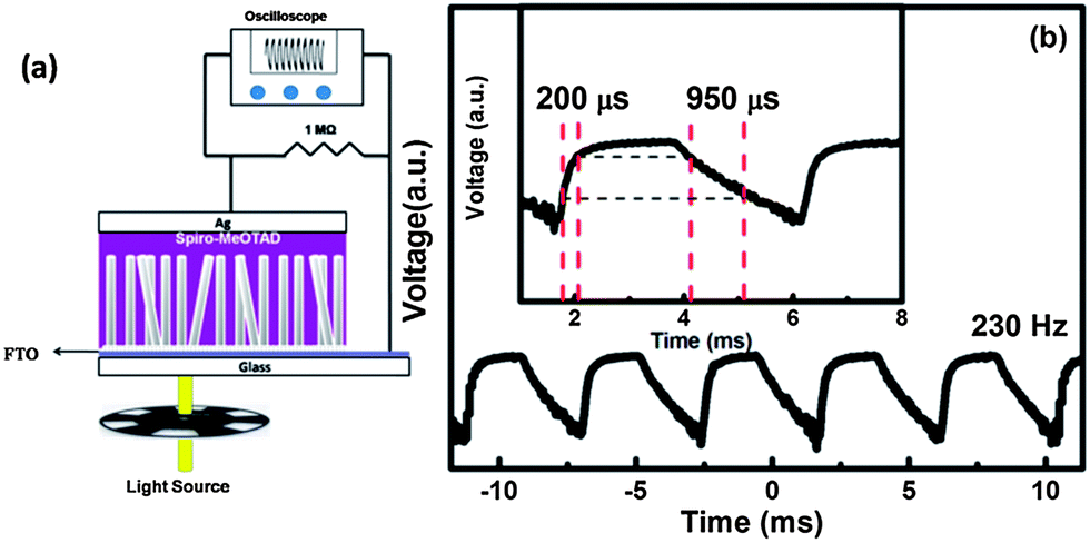 | ||
| Fig. 3 (a) Schematic of the experimental arrangement used to measure the response time of the photodiode, (b) photovoltage generated across 1 MΩ resistor under pulsating light of frequency 230 Hz. | ||
N:ZnO–SpiroMeOTAD visible photodiode
Photodetectors with response in the visible region are also important for various applications such as environmental monitoring, optical communications, and conventional or biomedical imaging.4 Recently, there has been a drive to replace the visible-light-sensitive toxic compounds such as CdS, CdSe, PbS with non-toxic, environment-friendly and earth abundant materials for application in visible light photodetection.35 Most of the recent efforts have been focused mainly on metal chalcogenides/nitrides/phosphides such as Bi2S3,36 Cu2ZnSnS4,17 InP,13 AgInS2 (ref. 11) etc. However, there have been only limited efforts on using the robust and eco-friendly metal oxide systems37,38 for visible light detection. Recently we reported39 that concurrent nitrogen and defect incorporation in ZnO can lead to a broadband absorption extending up to 650 nm, which also yields enhanced performance in photo-electrochemical (PEC) water splitting. Although undoped/doped ZnO alone is capable of sensing UV/visible light, these photodetectors require some applied potential for their operation and their response time is in few hundreds of seconds,1 as the working principle mostly involves adsorption–desorption of oxygen. Therefore, it is necessary to form a hybrid junction with N:ZnO which can sense visible light with very fast response. We have previously39 shown (in the context of PEC water splitting) that a simple addition of ammonia solution during the growth ZnO nanorods can lead to formation of Zn–nitrogen complex which, on heating in air leads to nitrogen doping within the ZnO lattice. We followed a similar approach in this work to grow the oriented nitrogen doped ZnO nanorods on FTO.The nitrogen doped ZnO (N:ZnO) grown in the presence of ammonia solution also showed oriented growth along [001] direction, as confirmed by XRD (inset Fig. 4(a)). The normalized absorbance data for ZnO and N:ZnO nanorod arrays in Fig. 4(a) explain the visual appearance of ZnO (white) and N:ZnO (orange-yellow). Interestingly, the N:ZnO film shows absorption below 650 nm, remarkably spanning more than half of the visible spectrum. The N2p states introduced by nitrogen doping and presence of other defects such as oxygen vacancies and zinc interstitials can explain the broadband absorption of N:ZnO.40 Nitrogen incorporation within ZnO lattice and other associated defect complexes are further confirmed by Raman spectroscopy which offers useful insights into the nature of defects and lattice disorder. Fig. 4(b) shows additional Raman modes at 279 c and 511 cm−1 in the case of N:ZnO which point towards successful incorporation of nitrogen within the ZnO lattice along with formation of a defect complex between the nitrogen dopant and zinc interstitials.40−42 This concurrent incorporation of dopant and defects in ZnO results in broadband absorption of N:ZnO. The Raman spectra of ZnO and N:ZnO are discussed in more details in the ESI-2.†
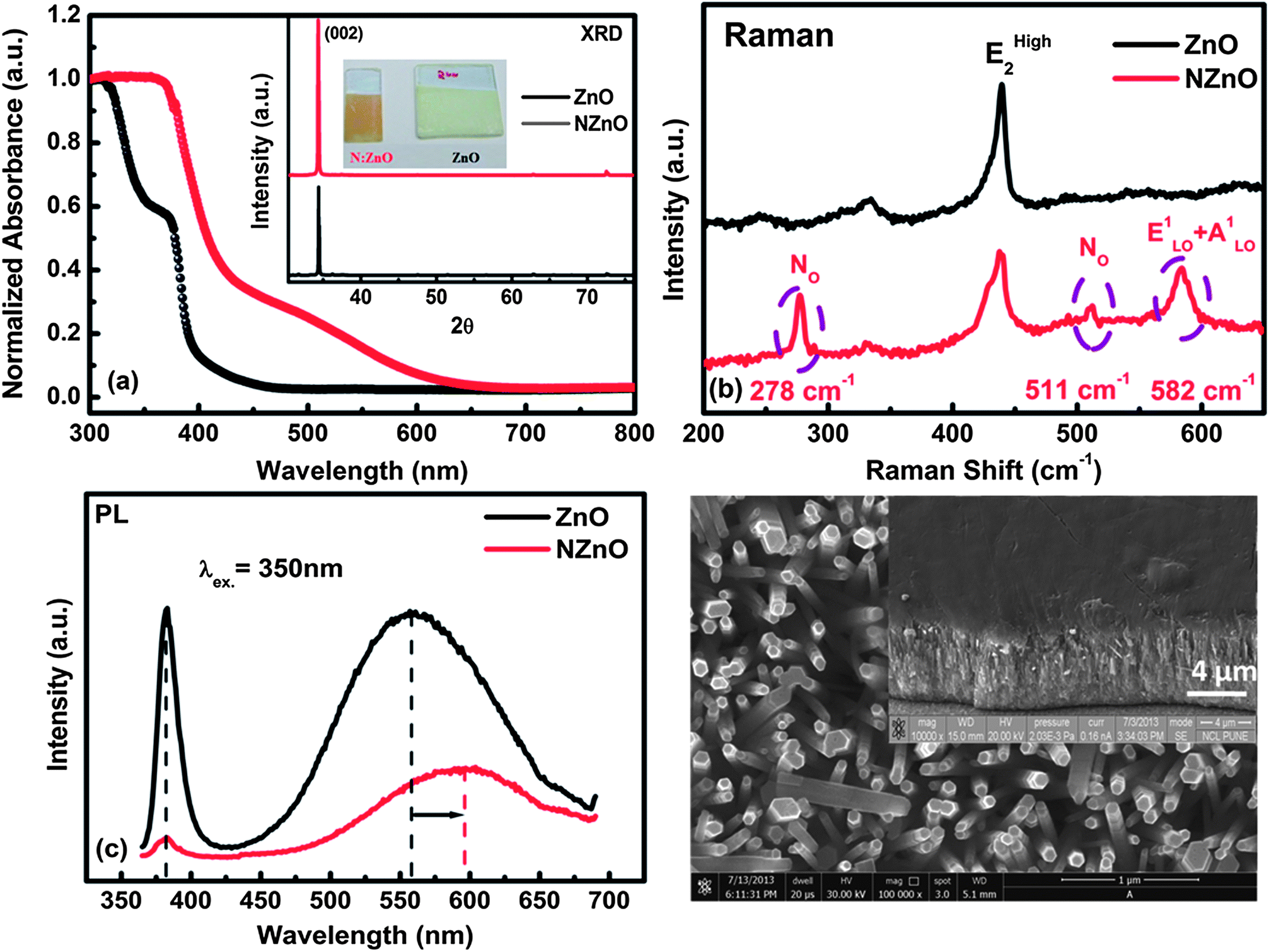 | ||
| Fig. 4 (a) UV-Vis absorbance and XRD of ZnO and N:ZnO nanorod arrays, (b) Raman comparison of ZnO and N:ZnO clearly pointing out the presence of N doping within ZnO, (c) photoluminescence (PL) spectrum of ZnO and N:ZnO films, (d) SEM images of N:ZnO nanorods and cross-sectional view of NZnO–SpiroMeOTAD photodiode. | ||
Fig. 4(c) shows the photoluminescence (PL) spectrum of ZnO and N:ZnO when excited at 350 nm (interband excitation). The ZnO case shows the near band edge emission at 380 nm with deep-level green luminescence which is usually assigned to defects such as oxygen vacancies or zinc vacancies. Interestingly, the PL of N:ZnO shows suppressed band edge luminescence and the defect-luminescence is unusually shifted to the orange region.43 The suppressed intensity of N:ZnO band edge luminescence can be attributed to the presence of nitrogen dopant levels near the valance band of ZnO which hinder the band to band transition and increase the intensity of the conduction band to defect level transition. The orange luminescence in N:ZnO can be assigned to the transition from the conduction band of N:ZnO to Oi or from Zi to Oi43 whose presence is also suggested by Raman spectroscopy.
Though various defects such as oxygen vacancies, zinc vacancies44,45etc. can lead to defect states within the energy gap of ZnO, it is important to identify the defects which can lead to broadband absorption of N:ZnO. First principle electronic structure calculations by Feng et al.40 on nitrogen doped ZnO have shown that nitrogen substitution for oxygen (NO) alone cannot explain the reduction in band gap of ZnO. Their calculations show that the defect complex between nitrogen substituting oxygen (NO), interstitial zinc (Zni) and oxygen vacancy (VO) gives rise to a defect band near the valance band which is formed by strongly coupled p-orbitals of anions (O and N) and d-states of Zni and host Zn atoms of the ZnO lattice. Importantly the defect band formed by 4NO–VO–Zni complex can touch and resonate with the valance band maxima of ZnO, thereby raising the valance band edge which results in a reduced band gap of ZnO. The presence of Raman mode at 279 cm−1 in N:ZnO in Fig. 4(b) is assigned to the stretching vibration of the defect complex between Zi and NO.42 The presence of Zi is further supported by the orange luminescence in N:ZnO which is assigned to the transition from Zi to oxygen interstitials.43 Therefore both Raman and photoluminescence data of N:ZnO point towards the presence of 4NO–VO–Zni complex which results in broadband absorption of N:ZnO up to 650 nm in the visible, thereby making it a good candidate for visible light photo-detection.
Substitutional doping of nitrogen in ZnO lattice has long been predicted to provide p type conductivity to ZnO. But the subject has remained controversial since no stable p-type nitrogen doped ZnO could be obtained or reproduced. Recent report on nitrogen doped ZnO nano-crystals46 also points out that air annealing at temperatures greater than 400 °C leads to oxygen vacancies and hence Zn-rich conditions, which gives n-type conductivity in ZnO despite nitrogen doping. Our N:ZnO samples were heated at 450 °C post-synthesis which explains the n-type behaviour in our N:ZnO nanorod arrays. The n-type behaviour in N:ZnO nanorods is also confirmed by the positive slope of electrochemical Mott–Schottky plot of N:ZnO (now added as ESI-4†). n-Type behaviour of N:ZnO therefore points towards the possibility of formation of rectifying junction with p-type Spiro-MeOTAD.
Fig. 4(d) shows the SEM image of oriented N:ZnO nanorod arrays grown on FTO. We fabricated an organic–inorganic hybrid photodiode for visible light detection using these oriented N:ZnO nanorods and Spiro-MeOTAD with the same architecture as was used for the undoped ZnO–SpiroMeOTAD photodiode case discussed earlier. The inset to Fig. 4(d) shows the 45° tilted view of N:ZnO–SpiroMeOTAD (N:ZnO–SPD) photodiode exhibiting good percolation of Spiro-MeOTAD within N:ZnO array.
The opto-electronic characterization was performed under illumination of white light LEDs with intensity of 18 mW cm−2. Fig. 5(a) shows the comparative J–V curves of ZnO and N:ZnO based photodiodes under dark and white light illumination. A rectifying behaviour is observed in the case on N:ZnO–SPD with a turn-on voltage of 0.2 V which is similar to ZnO–SPD. n-Type behaviour of N:ZnO therefore suggests that the Fermi energy of N:ZnO should be near the conduction band of ZnO. This is also in accordance with the previous experimental results by Perkins et al.47 who carried out ultraviolet photo-electron spectroscopy (UPS) on nitrogen doped ZnO thin films and observed that the Fermi energy lies very close to the conduction band for nitrogen doped ZnO explaining its n-type behaviour. Thus, as emphasized by Perkins et al., although nitrogen related defect complexes introduce a defect band near the valance band, they do not cause any appreciable change in the Fermi energy of ZnO. A magnified view of the J–V curve near zero bias (inset to Fig. 6(a)) clearly shows a small photovoltaic effect (Voc ∼ 0.1 V; Jsc ∼ 80 μA cm−2) for the case of N:ZnO–SPD, whereas no clear photoresponse was observed in the case of ZnO–SPD. This clearly points towards applicability of N:ZnO–SPD as an effective visible-light photodetector. Fig. 5(b) shows the dark and under-illumination curves of N:ZnO–SPD plotted on the semilog scale. The dark J–V curve shows a high rectification ratio of 103 at ±0.5 V. An order of magnitude increase in the rectification ratio of N:ZnO–SPD in comparison with ZnO–SPD can be attributed to smaller reverse leakage current due to a dense layer of N:ZnO near FTO (evident in the inset to Fig. 4(d)) which prevents direct electrical contact between Spiro-MeOTAD and FTO. Therefore, such a blocking layer reduces recombination at this interface, which also results in 300% improvement in Voc (0.1 V) of N:ZnO–SPD as compared to ZnO–SPD (0.026 V).
 | ||
| Fig. 5 (a) J–V curves of ZnO–SPD and N:ZnO–SPD under white light LED illumination of 18 mW cm−2, inset shows a magnified view of J–V curve near zero bias, (b) dark and white light (18 mW cm−2) J–V curve of N:ZnO–SPD plotted on the absolute semilog scale, (c) photo-response of N:ZnO–SPD under 18 mW cm−2 white light illumination under alternate on and off cycles, (d) energy diagram of N:ZnO–SPD showing photocurrent action under visible light illumination. | ||
 | ||
| Fig. 6 (a) Photo-response of NZnO–SPD under 13 mW cm−2 blue (460 nm), green (530 nm) and red (625 nm) illumination under alternate on and off cycles, (b) responsivity comparison of ZnO–SPD and N:ZnO–SPD. | ||
It can also be seen from Fig. 5(b) that the N:ZnO–SPD shows maximum sensitivity (Iphoto/Idark) of 103 near zero bias, supporting its self-powered mode of operation. This is further verified by measuring the photocurrent of N:ZnO–SPD at zero applied bias under a pulsating white light source at an interval of 10 s. The photocurrent density vs. time graph plotted on the semilog scale (Fig. 5(c)) also shows high photosensitivity of 103 with a photocurrent density of 80 μA cm−2 under 18 mW cm−2 of white LED illumination. This visible light response of N:ZnO can be explained on the basis of energy band diagram shown in Fig. 5(d). Nitrogen doping in ZnO introduces a band due to N2p levels near the valance band of ZnO, which results in broadband absorption of N:ZnO. Importantly the absorption onset in N:ZnO starts from 650 nm which corresponds to a position 1.9 eV below the conduction band whereas the Spiro-MeOTAD HOMO lies 1 eV below the conduction band of ZnO. Therefore, the Spiro-MeOTAD HOMO lies more than 1 eV higher in energy than the defect levels introduced by nitrogen doping in ZnO. Thus, light with wavelength in the visible region (400 nm < λ < 650 nm) can excite electrons from defect levels to the conduction band of ZnO and the photogenerated holes in defect levels can be further transferred to Spiro-MeOTAD HOMO because of favorable energy alignment. The visible light photo-response shown by N:ZnO–SPD proves the participation of defect levels in photocurrent generation.
In order to further investigate the visible photoresponse of N:ZnO–SPD we measured the photo-response under blue (455 nm), green (530 nm) and red (625 nm) LED illuminations.
From Fig. 6(a) it can be seen that the N:ZnO–SPD exhibits high photocurrent densities of 82, 50 and 10 μA cm−2 under blue, green and red illumination (intensity 13 mW cm−2), respectively. A reasonably high photoresponse even under red illumination agrees well with the broadband absorption spectrum of N:ZnO nanorod arrays. The spectral response of N:ZnO–SPD over the wavelength range of 350 to 800 nm was then plotted in terms of responsivity which is calculated using the relation R(λ) = EQE/hν. Fig. 6(b) shows the responsivity of N:ZnO–SPD in comparison with ZnO–SPD. It can be clearly seen that ZnO–SPD is active only in the UV region with UV to visible rejection ratio of 102 whereas N:ZnO–SPD clearly shows a peak responsivity of 6.5 mA W−1 at 470 nm, which extends deep into the visible region up to 650 nm. Importantly, the N:ZnO–SPD shows less responsivity under UV illumination even though both N:ZnO and Spiro-MeOTAD can absorb in the UV region. This can be understood by considering the device structure in which light (UV/Vis) enters from the FTO side. Firstly, strong absorption of FTO between 350 and 370 nm leads to absorption of the majority of photons of these wavelengths near this interface. Secondly, the presence of ammonia in the growth solution of N:ZnO nanorod arrays leads to the formation of a dense layer of N:ZnO NRs near FTO which can be as thick as 1–2 μm. Such dense layer of N:ZnO near FTO allows less amount of Spiro-MeOTAD to percolate through it thereby avoiding direct contact between Spiro-MeOTAD and FTO which results in the high rectification ratio. But the inadequate amount of hole transport material in this layer leads to higher recombination at this interface where most of the UV light is absorbed. Thus, the responsivity of N:ZnO–SPD in the spectral region from 370 to 400 nm is lower as compared to undoped ZnO–SPD. Light with wavelengths longer than 400 nm requires higher absorption length, therefore these wavelengths can penetrate deep within the film structure without being completely absorbed at the dense layer. Therefore, for λ > 400 nm the photo-action takes place in the region with adequate hole transport material resulting in efficient electron hole separation and higher responsivity in the visible region. Broad band responsivity of N:ZnO–SPD makes it an excellent candidate for white light sensing.
Optoelectronic applications of visible photodetectors also need fast response times. The response time of N:ZnO–SPD was measured in the same manner as the ZnO–SPD using an oscilloscope equipped with a pulsating source of light. Importantly, N:ZnO–SPD also shows a fast photoresponse in the millisecond time region as shown in Fig. 7. More specifically, we observed a rise time of 4 ms and a decay time of 10 ms for the case of N:ZnO–SPD. These values are slightly higher than those for the undoped ZnO–SPD which can be attributed to the trapping events of carriers in the trap states introduced by doping which can lead to slower diffusion of carriers leading to higher rise and decay times. Also due to higher length of N:ZnO rods, carriers have to travel a larger distance to reach the respective electrodes without getting recombined, thereby giving higher rise and decay times as compared to ZnO–SPD.
 | ||
| Fig. 7 Photo-response of N:ZnO–SPD under light pulses of 40 Hz. Inset shows the rise time and decay time of N:ZnO–SPD. | ||
High responsivity of N:ZnO–SPD in the visible region makes it possible to use it for sensing very low intensity white light. In order to verify this we measured the photo-response of N:ZnO–SPD in a room equipped with fluorescent tube lights emitting white light with intensity 28 μW cm−2. As shown in Fig. 8 and Fig. 9 even under this low intensity white light N:ZnO–SPD showed a photocurrent of 120 nA cm−2 with a high sensitivity of 102.
 | ||
| Fig. 8 Photo-response of N:ZnO–SPD under ambient white light of the fluorescent tube. | ||
 | ||
| Fig. 9 (a) Current of N:ZnO–SPD under dark, (b) photocurrent generated by N:ZnO–SPD under ambient room light equipped with fluorescent tubes giving white light of intensity ∼120 Lux (28 μW cm−2). A clear photocurrent response of two orders of magnitude is observed at zero applied bias supporting its self-powered mode of application for ambient light. | ||
We have given a comparative chart of recently reported organic–inorganic hybrid visible light self-powered photodetectors in Table 1. The N:ZnO–SPD also shows Iphoto/Idark ratio of 1600 and faster photoresponse (τrise −4 ms and τfall −10 ms) which represents at least one order magnitude improvement as compared to other hybrid visible photodetectors. The overall enhancement in the photocurrent and sensitivity is dramatic considering that N:ZnO–SPD involves nitrogen-doped ZnO as the only visible light sensing entity, whereas other (Table 1) hybrid photodetectors involve both organic and inorganic components which respond in the visible region. This enhancement can be attributed to favorable energy alignment between N:ZnO/Spiro-MeOTAD resulting in efficient carrier collection and transport by Spiro-MeOTAD. Most importantly, the performance of N:ZnO–SPD is better or comparable even to the conventional visible light sensors such as CdS and CdSe, thereby eliminating the need for using these toxic elements for visible light sensing.
| Photo-detector (ref.) | Bias | Wavelength and intensity | Dark current (density) | Photo-current (density) | I photo/Idark ratio | Rise time | Decay time |
|---|---|---|---|---|---|---|---|
| N:ZnO–SpiroMeOTAD (this report) | 0 V | White light 18 mW cm−2 | 6 nA (0.05 μA cm−2) | 9.6 μA (80 μA cm−2) | 1600 | 4 ms | 10 ms |
| CuInSe2:P3HT14 | 0.4 V | White light 7.6 mW cm−2 | 0.15 pA (0.3 × 10⁻³ μA cm−2) | 17 pA (0.38 μA cm−2) | 113 | — | — |
| Cu2ZnSnS4:P3HT17 | 0.4 V | White light 7.6 mW cm−2 | 0.012 pA (0.3 × 10⁻³ μA cm−2) | 2.23 pA (0.05 μA cm−2) | 150 | — | — |
| Ge:P3HT16 | 10 V | White light 8 mW cm−2 | 0.05 pA | 7.8 pA | 156 | — | — |
| AgInS2:P3HT11 | 2 V | UV 365 nm 2 mW cm−2 | 4 nA | 60 nA | 15 | — | — |
| CdS:polyaniline28 | 20 V | 420 nm 5.2 mW cm−2 | 0.2 μA | 1.2 μA | 6 | — | — |
| CdSe:P3HT (flexible substrate)15 | 3 V | White light 140 mW cm−2 | 30 pA | 16 nA | 500 | 10 ms | 10 ms |
| InP:P3HT13 | 0 V | AM 1.5 Sun light 100 mW cm−2 | — | 3.3 μA cm−2 | — | — | — |
| ZnO–rGO27 | 0 V | White light 80 mW cm−2 | 0.2 nA | 90 nA | 430 | 200 ms | 200 ms |
According to the Materials Safety Data Sheet (MSDS) from Sigma Aldrich, Spiro-TAD is considered to be a substance with very low levels of hazards as compared to other p-type semiconductors such as CuSCN. Unfortunately, there are no detailed studies on the toxicity of Spiro-MeOTAD. Therefore, in order to evaluate and compare the toxicity of Spiro-MeOTAD Vis a Vis cadmium based p-type semiconductors such as CdTe we carried out a comparative cyto-toxicity study on Spiro-MeoTAD and CdTe quantum dots with human hepatoma cell line (ESI-3†). The Spiro-MeOTAD is found to be 60–70% less toxic as compared to CdTe. Although use of completely non-toxic p-type organic semiconductor will be ideal, we believe that our demonstration of ZnO–SpiroMeOTAD photodiode with excellent properties (fast response, broad wavelength range etc.) is an important step towards environment friendly visible photo-detector designs.
Conclusion
In summary, we report a facile solution based fabrication of a self-powered organic–inorganic hybrid photodetector using nanorods of environmentally-friendly and earth-abundant metal oxide semiconductor n-type ZnO and an organic p-type semiconductor Spiro-MeOTAD. Initially, we fabricated a visible blind UV photodiode using undoped ZnO nanorod arrays impregnated with Spiro-MeOTAD. Such UV photodetector shows a UV to visible rejection ratio of 102 with a high photocurrent density of 50 μA cm−2 under a low intensity (3 mW cm−2) UV illumination. A rapid photoresponse with rise time of 200 μs and decay time 950 μs is observed in the case of undoped ZnO–SpiroMeOTAD UV photodiode.Importantly, we further show that a slight modification in the reaction conditions (doping nitrogen in ZnO nanorods) can covert the UV operative ZnO–Spiro-MeOTAD junction to be highly responsive even in the visible region (400–650 nm). The incorporation of nitrogen within ZnO causing broadband absorption (up to 650 nm) of N:ZnO was confirmed using Raman and UV-Vis absorption spectroscopy. The N:ZnO–SpiroMeOTAD photodiode shows a rapid and strong photoresponse under blue (460 nm), green (530 nm) and red (635 nm) LED illuminations, thereby making it capable of sensing white light. Interestingly, this self-powered visible photodetector shows a high photocurrent density of 120 nA cm−2 under low intensity (28 μW cm−2) white light. The photosensing parameters of N:ZnO–SpiroMeOTAD photodiode are much superior to previously reported organic–inorganic hybrid photo-detectors. High visible light sensitivity of N:ZnO makes it an attractive alternative over toxic element (Cd, Pb) based current visible light photodetectors.
Acknowledgements
O.G. would like to thank the Council of Scientific and Industrial Research (CSIR) for Senior Research Fellowship (SRF). U.S .and T.K. would like to thank the Director, Indian Institute of Science Education and Research (IISER), Pune for permission to do research internship at the National Chemical Laboratoty (CSIR-NCL), Pune. The authors also thank Pooja Singh for carrying out cytotoxicity studies on Spiro-MeOTAD.References
- L. Peng, L. Hu and X. Fang, Adv. Mater., 2013, 25, 5321–5328 CrossRef CAS PubMed.
- T. Zhai, X. Fang, M. Liao, X. Xu, H. Zeng, B. Yoshio and D. Golberg, Sensors, 2009, 9, 6504–6529 CrossRef CAS PubMed.
- X. Li, C. Gao, H. Duan, B. Lu, Y. Wang, L. Chen, Z. Zhang, X. Pan and E. Xie, Small, 2013, 9, 2005–2011 CrossRef CAS PubMed.
- G. Konstantatos and E. H. Sargent, Nat. Nanotechnol., 2010, 5, 391–400 CrossRef CAS PubMed.
- B. J. Hansen, Y. Liu, R. Yang and Z. L. Wang, ACS Nano, 2010, 4, 3647–3652 CrossRef CAS PubMed.
- Y. Q. Bie, Z. M. Liao, H. Z. Zhang, G. R. Li, Y. Ye, Y. B. Zhou, J. Xu, Z. X. Qin, L. Dai and D. P. Yu, Adv. Mater., 2011, 23, 649–653 CrossRef CAS PubMed.
- D. Wu, Y. Jiang, Y. G. Zhang, Y. Q. Yu, Z. F. Zhu, X. Z. Lan, F. Z. Li, C. Y. Wu, L. Wang and L. B. Luo, J. Mater. Chem., 2012, 22, 23272–23276 RSC.
- X. S. Fang, Y. Bando, M. Y. Liao, T. Y. Zhai, U. K. Gautam, L. Li, Y. Koide and D. Golberg, Adv. Funct. Mater., 2010, 20, 500–508 CrossRef CAS.
- Z. W. Gao, W. F. Jin, Y. Zhou, Y. Dai, B. Yu, C. Liu, W. J. Xu, Y. P. Li, H. L. Peng, Z. F. Liu and L. Dai, Nanoscale, 2013, 5, 5576–5581 RSC.
- T. Y. Zhai, X. S. Fang, M. Y. Liao, X. J. Xu, L. Li, B. D. Liu, Y. Koide, Y. Ma, J. N. Yao, Y. Bando and D. Golberg, ACS Nano, 2010, 4, 1596–1602 CrossRef CAS PubMed.
- M. J. Deng, S. L. Shen, X. W. Wang, Y. J. Zhang, H. R. Xu, T. Zhang and Q. B. Wang, CrystEngComm, 2013, 15, 6443–6447 RSC.
- S. Mridha and D. Basak, Appl. Phys. Lett., 2008, 92, 142111 CrossRef.
- C. J. Novotny, E. T. Yu and P. K. L. Yu, Nano Lett., 2008, 8, 775–779 CrossRef CAS PubMed.
- J. J. Wang, Y. Q. Wang, F. F. Cao, Y. G. Guo and L. J. Wan, J. Am. Chem. Soc., 2010, 132, 12218–12221 CrossRef CAS PubMed.
- X. F. Wang, W. F. Song, B. Liu, G. Chen, D. Chen, C. W. Zhou and G. Z. Shen, Adv. Funct. Mater., 2013, 23, 1202–1209 CrossRef CAS.
- D. J. Xue, J. J. Wang, Y. Q. Wang, S. Xin, Y. G. Guo and L. J. Wan, Adv. Mater., 2011, 23, 3704–3707 CrossRef CAS PubMed.
- J. J. Wang, J. S. Hu, Y. G. Guo and L. J. Wan, Npg Asia Mater., 2012, 4, e2 CrossRef.
- L. Schmidt-Mende and J. L. MacManus-Driscoll, Mater. Today, 2007, 10, 40–48 CrossRef CAS.
- H. S. Kim, C. R. Lee, J. H. Im, K. B. Lee, T. Moehl, A. Marchioro, S. J. Moon, R. Humphry-Baker, J. H. Yum, J. E. Moser, M. Gratzel and N. G. Park, Sci. Rep., 2012, 2, 591 Search PubMed.
- L. A. Duan, L. D. Hou, T. W. Lee, J. A. Qiao, D. Q. Zhang, G. F. Dong, L. D. Wang and Y. Qiu, J. Mater. Chem., 2010, 20, 10946 RSC.
- S. J. Moon, Y. Itzhaik, J. H. Yum, S. M. Zakeeruddin, G. Hodes and M. Gratzel, J. Phys. Chem. Lett., 2010, 1, 1524–1527 CrossRef CAS.
- L. Yang, U. B. Cappel, E. L. Unger, M. Karlsson, K. M. Karlsson, E. Gabrielsson, L. C. Sun, G. Boschloo, A. Hagfeldt and E. M. J. Johansson, Phys. Chem. Chem. Phys., 2012, 14, 779–789 RSC.
- S. M. Hatch, J. Briscoe and S. Dunn, Adv. Mater., 2013, 25, 867–871 CrossRef CAS PubMed.
- H. G. Li, G. Wu, M. M. Shi, L. G. Yang, H. Z. Chen and M. Wang, Appl. Phys. Lett., 2008, 93, 153309 CrossRef.
- S. X. Yang, J. Gong and Y. L. Deng, J. Mater. Chem., 2012, 22, 13899–13902 RSC.
- S. X. Yang, J. Gong and Y. L. Deng, J. Mater. Chem., 2012, 22, 24522–24525 RSC.
- Z. Y. Zhan, L. X. Zheng, Y. Z. Pan, G. Z. Sun and L. Li, J. Mater. Chem., 2012, 22, 2589–2595 RSC.
- H. W. Lin, H. B. Liu, X. M. Qian, S. W. Lai, Y. J. Li, N. Chen, C. B. Ouyang, C. M. Che and Y. L. Li, Inorg. Chem., 2011, 50, 7749–7753 CrossRef CAS PubMed.
- C. Xu, P. Shin, L. Cao and D. Gao, J. Phys. Chem. C, 2009, 114, 125–129 Search PubMed.
- A. Yengantiwar, R. Sharma, O. Game and A. Banpurkar, Curr. Appl. Phys., 2011, 11, S113–S116 CrossRef PubMed.
- A. Bera, H. Peng, J. Lourembam, Y. Shen, X. W. Sun and T. Wu, Adv. Funct. Mater., 2013, 23, 4977–4984 CrossRef CAS.
- P. N. Ni, C. X. Shan, S. P. Wang, X. Y. Liu and D. Z. Shen, J. Mater. Chem. C, 2013, 1, 4445–4449 RSC.
- Y.-Y. Lin, C.-W. Chen, W.-C. Yen, W.-F. Su, C.-H. Ku and J.-J. Wu, Appl. Phys. Lett., 2008, 92, 233301 CrossRef.
- S. M. Hatch, J. Briscoe, A. Sapelkin, W. P. Gillin, J. B. Gilchrist, M. P. Ryan, S. Heutz and S. Dunn, J. Appl. Phys., 2013, 113, 204501 CrossRef.
- J. J. Wang, J. S. Hu, Y. G. Guo and L. J. Wan, J. Mater. Chem., 2011, 21, 17582–17589 RSC.
- G. Konstantatos, L. Levina, J. Tang and E. H. Sargent, Nano Lett., 2008, 8, 4002–4006 CrossRef CAS PubMed.
- N. Kouklin, Adv. Mater., 2008, 20, 2190–2194 CrossRef CAS.
- R. R. Prabhakar, N. Mathews, K. B. Jinesh, K. R. G. Karthik, S. S. Pramana, B. Varghese, C. H. Sow and S. Mhaisalkar, J. Mater. Chem., 2012, 22, 9678–9683 RSC.
- O. Game, U. Singh, A. A. Gupta, A. Suryawanshi, A. Banpurkar and S. Ogale, J. Mater. Chem., 2012, 22, 17302–17310 RSC.
- Y. H. Lu, S. P. Russo and Y. P. Feng, Phys. Chem. Chem. Phys., 2011, 13, 15973–15976 RSC.
- N. Ashkenov, B. N. Mbenkum, C. Bundesmann, V. Riede, M. Lorenz, D. Spemann, E. M. Kaidashev, A. Kasic, M. Schubert, M. Grundmann, G. Wagner, H. Neumann, V. Darakchieva, H. Arwin and B. Monemar, J. Appl. Phys., 2003, 93, 126–133 CrossRef CAS.
- F. Friedrich, M. A. Gluba and N. H. Nickel, Appl. Phys. Lett., 2009, 95, 141903 CrossRef.
- M. Willander, O. Nur, J. R. Sadaf, M. I. Qadir, S. Zaman, A. Zainelabdin, N. Bano and I. Hussain, Materials, 2010, 3, 2643–2667 CrossRef CAS.
- G. Z. Xing, Y. H. Lu, Y. F. Tian, J. B. Yi, C. C. Lim, Y. F. Li, G. P. Li, D. D. Wang, B. Yao, J. Ding, Y. P. Feng and T. Wu, AIP Adv., 2011, 1, 022152 CrossRef.
- B. Y. Zhang, B. Yao, Y. F. Li, A. M. Liu, Z. Z. Zhang, B. H. Li, G. Z. Xing, T. Wu, X. B. Qin, D. X. Zhao, C. X. Shan and D. Z. Shen, Appl. Phys. Lett., 2011, 99, 182503 CrossRef.
- B. Chavillon, L. Cario, A. Renaud, F. Tessier, F. Cheviré, M. Boujtita, Y. Pellegrin, E. Blart, A. Smeigh, L. Hammarström, F. Odobel and S. Jobic, J. Am. Chem. Soc., 2011, 134, 464–470 CrossRef PubMed.
- C. L. Perkins, S.-H. Lee, X. Li, S. E. Asher and T. J. Coutts, J. Appl. Phys., 2005, 97, 034907 CrossRef.
Footnote |
| † Electronic supplementary information (ESI) available: SI-1: response time measurements of self powered hybrid ZnO–SPD under nanosecond pulsed UV laser, SI-2: Raman analysis of N:ZnO and ZnO SI-3: cytotoxicity study on Spiro-MeOTAD SI-4: electrochemical Mott–Schottky plots of ZnO and N:ZnO. See DOI: 10.1039/c3nr04727j |
| This journal is © The Royal Society of Chemistry 2014 |