A twin-free single-crystal Ag nanoplate plasmonic platform: hybridization of the optical nano-antenna and surface plasmon active surface†
Hyoban
Lee‡
a,
Kwang-Yong
Jeong‡
b,
Taejoon
Kang
ac,
Min-Kyo
Seo
*bd and
Bongsoo
Kim
*ad
aDepartment of Chemistry, KAIST, Daejeon 305-701, Korea. E-mail: bongsoo@kaist.ac.kr
bDepartment of Physics, KAIST, Daejeon 305-701, Korea. E-mail: minkyo_seo@kaist.ac.kr
cBioNanotechnology Research Center, KRIBB, Daejeon 305-806, Korea
dKAIST Institute for the NanoCentury, KAIST, Daejeon 305-701, Korea
First published on 25th October 2013
Abstract
Surface plasmons based on metallic nanostructures enable light manipulation beyond the optical diffraction limit. We have epitaxially synthesized twin-free single-crystal Ag nanoplates on SrTiO3 substrates. Unlike the nanoplates synthesized in a solution phase, these nanoplates have perfectly clean surfaces as well as a quite large size of tens of micrometers. As-synthesized defect-free single-crystal Ag nanoplates have an atomically flat surface and sides with well-defined angles, allowing long distance propagation of surface plasmons and highly reliable plasmonic integration. By spatially separating receiving and transmitting antennas and plasmonically interfacing them, the signal quality of transmission/reception can be largely improved. Furthermore, by combining sub-dimensional nanostructures onto the two-dimensional space effective hierarchical plasmonic nano-complexes can be built up. Theoretical simulations well reproduced unique experimental results of coupling between SPPs and free-space radiation by the nanoplate antenna sides, low-loss long-range SPP propagation, and tunneling or scattering of SPPs at a nano-gap as well as a nano-structure introduced on the nanoplate. The single-crystal Ag nanoplate will find superb applications in plasmonic nano-circuitry and lab-on-a-chip for biochemical sensing.
1. Introduction
Metallic nano-objects support collective electron oscillations known as surface plasmons and can thereby strongly concentrate electromagnetic fields into a deep sub-wavelength scale area.1–5 These highly localized fields can extremely enhance linear and nonlinear light-matter interactions and allow superb applications in nano-optical sensing,6–8 high resolution imaging,9,10 and nonlinear signal conversion11 beyond conventional optics based on dielectric materials. Particularly, plasmonic optical nano-antennas efficiently interface propagating radiation with nanoscale target materials as small as colloidal quantum dots or fluorescent molecules.6–10,12–15 Surface plasmon polaritons (SPPs) existing on the metal/dielectric interface have been also widely employed in diverse devices including plasmonic optoelectronic nano-devices16–19 and surface plasmon resonance (SPR) based biochemical sensors.20,21 Although various plasmonic elements have been demonstrated, there still remains the quest for a dressed metallic nano-structure, which can naturally involve plasmonic nano-antennas and a SPP-active surface and integrate the best of both worlds.Recently, nanoplates of various compositions have been widely investigated for flexible thin-film transistors,22 Li-ion batteries,23,24 transistor sensors,25in vivo imaging,26 and topological insulators.27 They are well suitable for individual patterning and characteristic measurement in contrast to nanoparticles which are quite small and easily aggregated.28,29 Especially, large-scale integrability is one of the key characteristic of nanoplates that have a large surface with nm level thickness,29 greatly enhancing practical versatility in application. Nevertheless, except employing nanoplate synthesized in a solution phase as a raw material for fabrication of plasmonic elements by focused ion beam (FIB) milling30 or for measurement of plasmonic local density of states by two-photon illumination,31 there has been little research to explore and examine single-crystalline metal nanoplates themselves as a plasmonic antenna or device. Recently, it was reported that nanoplates synthesized in a solution phase with a size of a few hundred nm provide localized surface plasmon resonances,32,33 which can be tuned by the nanoplate size. The Ag nanoplates of a large size of tens of micrometers as reported here can support and interface optical antenna resonances and propagating SPPs at the same time to make a more versatile plasmonic platform.
In this study, we have demonstrated a 2-dimensional plasmonic nano-platform merging surface plasmonic active-surface and nano-antennas on a built-in system by employing a single-crystal Ag nanoplate and investigated its plasmonic properties in the Fresnel region with an optical microscope. Typical metal layers formed by conventional methods such as thermal or electron beam evaporation and focused ion beam or electron-beam lithography generally have inhomogeneous multi-crystal domains and rough surfaces at the atomic scale.34,35 Such imperfections cause considerable scattering and dephasing of surface plasmons, thereby preventing us from constructing an ideal plasmonic assembly comprising of thus-fabricated metal nanoplates. In contrast, the Ag nanoplates synthesized by the vapor transport method at a very high temperature have single crystal structures with an atomically flat surface, realizing highly reliable plasmonic antenna operations that agree well with predictions by full field electromagnetic simulations. Furthermore, single crystal Ag nanoplates as large as tens of micrometers can be grown epitaxially in a well-defined orientation with respect to the substrate by a vapor transport method, whereas sizes of Ag nanoplates prepared by typical liquid phase synthesis are limited to a few micrometers.
Since a 2-dimensional plasmonic nano-platform can spatially separate components having distinct functions and plasmonically interface them, it can highly improve the efficiency of transmission/reception of the optical signal. Furthermore, by combining sub-dimensional nanostructures onto the 2-dimensional space it can build up effective hierarchical plasmonic nano-complexes. We anticipate that the Ag nanoplate, which has no interband transition at visible wavelength and thus can provide good plasmonic nano-optical performances in a wide spectral range,36,37 would contribute to diverse nano-optical applications including biochemical sensors employing surface-enhanced Raman scattering (SERS) and fluorescent materials.
2. Experimental section
2.1 Synthesis of Ag nanoplates
We placed a Ag slug in an alumina boat at the middle of a 1 in. diameter horizontal quartz tube furnace (ESI, Fig. S1†). The Ag slug was heated to 820–840 °C and then the carrier gas transports Ag vapor to the lower temperature region, where Ag nanoplates were grown on a SrTiO3 (001) substrate. The distance from the center of a heating zone to the substrate was 5 cm and the Ar gas flowed at a rate of 100 sccm, maintaining the chamber pressure in a range of 2–5 torr. The reaction time was ∼20 min.2.2 Optical-microscope setup for measurements of SPPs on Ag nanoplates
Employing a microscope-based measurement set-up (Fig. 2c), we examined the performance of a Ag nanoplate as a converged plasmonic platform. A dry 100× objective lens with a numerical aperture of 0.7 focuses the laser beam on one side of the Ag nanoplate acting as a receiving antenna, and simultaneously collects output radiation from the other side acting as a transmitting antenna. The characteristics of SPP generation and plasmonic antenna radiation were investigated using a charge-coupled device (CCD) camera. The polarization state of the output radiation from the Ag nanoplate was resolved by a linear polarizer placed in front of the CCD camera. Another linear polarizer and a half-wave plate controlled the polarization state of incident light from a continuous-wave HeNe laser with 632.8 nm wavelength. We placed a single Ag nanoplate onto a Si substrate using a homebuilt nano-manipulator consisting of a tungsten tip (∼100 nm diameter at the end) mounted on a three-axes piezoelectric stage.2.3 FDTD simulation
The metal was modelled with a Drude model: ε(ω) = ε∞ − ωp2/(ω2 + iγω). By fitting the experimentally determined dielectric function of Ag in the spectral range of 580–700 nm, the background dielectric constant ε∞, plasma frequency ωp and collision frequency γ at room temperature were set as 3.35, 1.38 × 10¹⁶ s−1, and 5.35 × 10¹³ s−1, respectively. The refractive index and extinction coefficient of the silicon substrate were set as 3.88 and 0.18, respectively, at 632.8 nm.2.4 Characterization
Field emission scanning electron microscopy images of a Ag nanoplate were taken on a Phillips XL30S. TEM and HRTEM images and SAED patterns were taken on a JEOL JEM-2100F transmission electron microscope operated at 200 kV. After Ag nanoplates were dispersed in ethanol, a drop of the solution was put on a holey carbon coated copper grid for TEM analysis.3. Results and discussion
3.1 Preparation of single-crystal Ag nanoplates
The single-crystal Ag nanoplates were synthesized by a simple vapor transport method using a Ag slug as a precursor (ESI, Fig. S1†). On a SrTiO3 (STO) (001) substrate, single-crystalline Ag nanoplates are grown epitaxially with truncated equilateral triangle geometry. The Ag nanoplates have side facet lengths from a few micrometers to tens of micrometers and a thickness of 100–200 nm depending on the reaction time. Fig. 1a and b are the 45° tilted-view scanning electron microscopy (SEM) image and top-view SEM image of the Ag nanoplates grown on a STO (001) substrate, respectively, showing inclined Ag nanoplate arrays, of which the bottom sides are mostly aligned along two lines perpendicular to each other. The high-resolution transmission electron microscopy (HRTEM) image shows distinct lattice fringes and selected area electron diffraction (SAED) patterns show a single set of fcc reflection, both clearly indicating the single-crystalline nature of the Ag nanoplates (Fig. 1c and d). The top crystal plane of the Ag nanoplate is a (111) plane.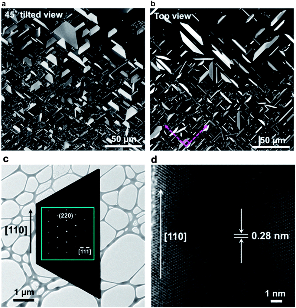 | ||
| Fig. 1 Ag nanoplates epitaxially grown on a STO (001) substrate having a truncated equilateral triangle geometry. (a) 45° tilted-view SEM image and (b) top-view SEM image of the Ag nanoplate arrays. (c) Low resolution TEM image and SAED pattern of the Ag nanoplate. The Ag nanoplate has a truncated equilateral triangle geometry and its main planes are {111} planes. (d) High resolution TEM image of a Ag nanoplate. | ||
3.2 Fabrication of Ag nanoplate optical nano-antenna
Fig. 2a shows a schematic of the single-crystal Ag nanoplate supporting a novel nano-optical stage which can naturally merge plasmonic nano-antennas and a SPP-active surface. Fig. 2b is the SEM image of an as-synthesized Ag nanoplate transferred onto a Si substrate. The side facet of the Ag nanoplate can act as a receiving antenna, converting the incident light to the SPPs propagating on the nanoplate surface. When the incident light focused on a receiving side is polarized perpendicular to the side, the in-coupling efficiency of the propagating SPPs is maximized, inducing strong plasmonic evanescent fields on the nanoplate surface. Strongly confined evanescent fields can superbly overlap with the active media such as target molecules attached on the nanoplate surface, and boost their optical response including surface enhanced Raman scattering, fluorescent emission, and second harmonic generation. The propagating SPPs would eventually re-radiate into the free-space at the opposite sides of the nanoplate, which can act as a separated transmitting antenna.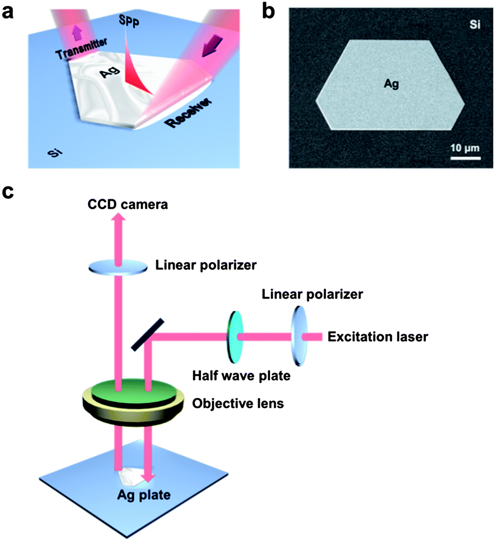 | ||
| Fig. 2 (a) The schematic of the Ag nanoplate providing plasmonic nano-antennas and SPP-active surface at the same time. (b) SEM image of a single-crystalline Ag nanoplate on the Si substrate. (c) The schematic of the optical microscope-based polarization-resolved measurement set-up. | ||
The properties of the transmitted radiation strongly affected the angle between the SPP propagation direction and the output side. Fluorescent or nonlinear signals from the target active materials excited by the SPP evanescent fields can also be out-coupled through the transmitting antenna and collected by conventional optics efficiently. Importantly, the spatial separation of the receiving and transmitting antennas can critically reduce noise due to undesired mixing of input and output signals. Such separation also minimizes heating in target materials caused by the incident laser. These superb properties of a Ag nanoplate plasmonic platform would help improve the quality of sensing ability, making them a potentially ideal plasmonic guiding platform.
It is remarkable that our single crystalline Ag nanoplates have atomically smooth surfaces (ESI, Fig. S2†), which cannot be achieved by conventional top-down nanofabrication techniques such as evaporated thin-film or electron-beam lithography. By minimizing scattering and dephasing of surface plasmons, the ultraflat surface allows ideal SPP propagations and supports a reliable plasmonic near-field playground. The atomically sharp and well-defined edges can conduct plasmonic antenna operations without random perturbations to signal reception and transmission processes due to surface defects. The interfacial angles of our Ag nanoplates are 60°, crystallographically fixed. The well-defined angles between all facetted sides help achieve extremely accurate alignment of the sides, functioning as the input and output antennas.
The truncated equilateral triangle shaped hexagon structure, being composed of three pairs of parallel opposite sides and having an interfacial angle of 60°, provides the neatest configuration of the plasmonic surface and antenna sides. Fig. 3a shows an optical microscope image of the examined Ag nanoplate with the laser beam focused on the longest side. A typical laser spot size was smaller than 1 μm. In order to maximize the coupling to SPPs propagating on the nanoplate surface, the incident laser is polarized perpendicular to the input side.
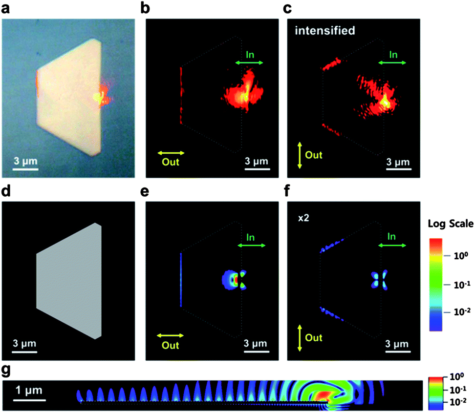 | ||
| Fig. 3 (a) Optical image of a truncated equilateral triangle shaped hexagonal Ag nanoplate focused by 632.8 nm laser light on the right side. (b and c) Polarization-resolved measurements of radiation distribution from the Ag nanoplate. The green arrows represent the polarization of the incident laser and yellow arrows represent the polarization direction of the linear polarizer in front of the CCD camera. (d) The truncated equilateral triangle shaped Ag nanoplate used in the calculations has exactly the same shape and size as used in experiments. (e and f) The calculated vertical component of time-averaged Poynting vector distributions captured at a plane 150 nm above the nanoplate surface. (g) Cross-sectional view of the calculated electrical field intensity distribution of SPPs propagating on the Ag nanoplate surface. | ||
3.3 Characteristics of the Ag nanoplate optical nano-antenna
When the incident light is received on the right side, coupled SPPs propagate on the surface and output antenna radiation is transmitted from the SPPs at the opposite left side of the Ag nanoplate, as shown in the polarization-resolved measurement of the coupling process (Fig. 3b). For the set-up observing Fig. 3b, the linear polarizer in front of the CCD was set perpendicular to the left side, detecting sizable transmitted radiation at the left side. When the polarizer was set parallel to the left side (Fig. 3c), however, the transmission at the left side was erased, and transmitted radiation was instead detected at the top and bottom inclined sides of the Ag nanoplate. This observation indicates that the transmitted radiation is polarized perpendicular to the output side and thus they originated from the SPPs of which evanescent electric fields are normal to the nanoplate surface. Here, SPPs are propagating from the receiving antenna side to the transmitting antenna side over a distance of ∼7.4 μm, which is long enough to support a multi-scale plasmonic playground for various nano-optical applications on the Ag nanoplate surface.4,9,10,13The modal characteristics of SPPs in a general asymmetric three-layer slab waveguide, made of Air/Ag/Si, can be completely described by a single dispersion equation,38 the propagation length and the evanescent field decay length being given by the solution of the dispersion equation. In the Air/Ag (100 nm thick)/Si waveguide as employed here, the propagation length of SPPs at 632.8 nm wavelength is calculated to be ∼81.7 μm, when the complex dielectric constants of Ag and Si are set as −18.2166 − 0.3871i and 15.1434 + 0.1398i, respectively. Such a long propagation length allows our Ag nanoplate to plasmonically mediate the input and output antenna sides successfully, separated by a few or even a few tens of micrometers. The SPP propagation length in this structure is longer than ∼79.4 μm in a typical Air/Ag interface because the thin Ag nanoplate absorbs SPPs less than the semi-infinite Ag layer. The vertical decay length of the evanescent fields is calculated to be ∼209 nm representing field confinement below the diffraction limit of half the wavelength.
In order to further understand the plasmonic characteristics of the Ag nanoplate, we performed full-field simulations using the finite-difference time-domain (FDTD) method.39Fig. 3e and f show vertical component distributions of the Poynting vectors from the Ag nanoplate. A focused Gaussian beam with a spot size of 500 nm is injected into the right side and coupled to SPPs propagating toward the left side. The polarization-resolved distributions of the vertical component of the Poynting vector were captured at a plane 150 nm above the nanoplate surface. The simulation result in Fig. 3e provides an excellent reproduction of the experimental results in Fig. 3b: the transmitted radiation is polarized perpendicular to the output side and fully separated from the scattered incident light. Furthermore, the cross-sectional view of the electrical field intensity profile clearly shows that SPPs are strongly bound onto the Ag/Air interface and propagate for a distance up to 7.4 μm between the receiving and transmitting antenna sides (Fig. 3g). By comparison, small nanoplates with a size of a few hundred nm support localized surface plasmon resonances instead of propagating SPPs.32,33 The coupling efficiency of the focused Gaussian incident light to the propagating SPPs is estimated to be ∼5.9% with the spot size set as 500 nm (ESI, Fig. S3†). In addition, the out-coupling efficiency of the transmitting antenna side is calculated to be ∼32% from the ratio of the SPP power incident to the output antenna side to the radiation power coupled to the air free-space. Indeed, the simulations show that even without any additional modification or optimization such as grating structures40 or angled light injection,41 the bare side of the nanoplate could be a good enough receiving and transmitting antenna between SPPs and free-space radiation. Notably, most of the out-coupled radiation from the nanoplate side propagates at an angle of ∼8° with respect to the nanoplate plane (ESI, Fig. S4†). Considering a very small propagation angle of this out-coupled radiation pattern, angled light injection could extensively increase the in-coupling efficiency according to the reciprocity theorem.42
Since the polarization of output radiation is always normal to the output side, we can selectively collect output radiation from a specific output side or eliminate signal from unwanted output sides by optimally adjusting the angle of the observation polarizer (Fig. 3). We note that this unique characteristic allows output signal detection only from the target materials attached on a selected output antenna side, and possibly from multiple targets on different locations of the plasmonic nanoplate. Precise agreement between the experimental and numerical radiation distributions (Fig. 3b, c, e and f) is found in most respects including the location of the radiation and the polarization properties. This excellent agreement suggests that the single-crystalline Ag nanoplate in experiments can be closely represented by the atomically precise ideal structure assumed in simulations.
A key feature of this study is that the Ag nanoplate nanoantenna platform can effectively interface the SPP evanescent field with target materials attached on the nanoplate. In order to further investigate this hypothesis, we examined SPP scattering behaviour by placing a Ag nanobelt on a Ag nanoplate (Fig. 4a). The width, thickness, and length of the nanobelt are 600 nm, 120 nm, and 5 μm, respectively. Since the SPPs are strongly bound to the metal surface, coupled to the free-space only at discontinuities on the nanoplate, the scattered radiation is constricted to the proximity of a nanobelt ∼12.7 μm away from the incident laser spot (Fig. 4b). The scattered radiation is polarized perpendicular to the side facet of the nanobelt, showing that the nanobelt acts as a plasmonic transmitting antenna and couples SPPs to free-space radiation. The observed properties can be best utilized to examine intrinsic characteristics of nanostructures or biochemical materials introduced on the surface, since background scattering noises can be highly suppressed in this scheme because of an atomically smooth surface. We thus expect that the Ag nanoplate will support a miniaturized SPR platform as an alternative to the conventional SPR platforms based on a wide metal film coupled to a large glass prism and also improve the sensitivity of SPR measurements. Numerical simulation employing a simplified structure, which includes a 120 nm thick Ag nanobelt located 5 μm away from the input antenna side on a Ag nanoplate, successfully reproduced the experimental scattering behaviours (Fig. 4c and d). In the simulation, the width and length of the nanobelt were set as 500 nm and 4 μm, respectively.
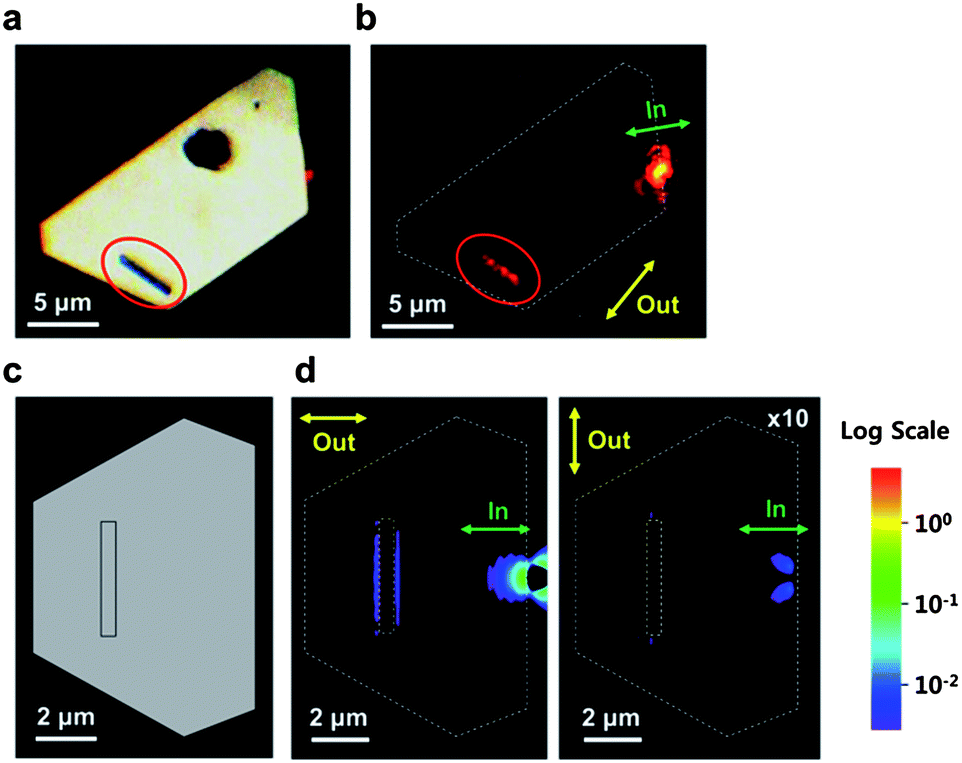 | ||
| Fig. 4 (a) Optical image of a Ag nanoplate involving a Ag nanobelt (inside the red circle) on the surface. (b) Scattering of SPPs by a nanobelt located on the Ag nanoplate surface. (c) The truncated equilateral triangle shaped Ag nanoplate and a Ag nanobelt used in the calculations. (d) The calculated vertical component of polarization-resolved time-averaged Poynting vector distributions. The nanobelt structure is superimposed on the radiation distribution. | ||
By attaching sub-dimensional nanostructures such as nanobelts or nanoparticles onto a nanoplate we can fabricate a remote SERS sensor.43 Since Raman signals are captured at the laser irradiated region in a conventional SERS experiment, the utilization of intense laser for distinct Raman signals has been limited for bio-medical materials such as living cells, fragile proteins, and unstable bio-chemical molecules. However, a remote-SERS sensor can significantly reduce direct damage of target materials due to strong incident laser by spatially separating the regions for laser irradiation and Raman signal emission. Nanoplates would be able to provide more diversified plasmonic assemblies than nanoparticle–nanowire junctions mainly employed for remote SERS sensors.44
In addition to placing nano-materials on the nanoplate, we can introduce FIB milled plasmonic nanostructures such as nano-scale gaps, grooves, and antennas onto the Ag nanoplate. Fig. 5a shows a Ag nanoplate involving a FIB milled 90 nm wide gap parallel to the two major sides of the trapezoid-shaped nanoplate. SPPs are coupled to the free-space at both the nano-gap and the output side opposite to the input side (Fig. 5b). This image clearly demonstrates that part of the SPPs tunnels through the nano-gap and reaches the opposite side of the nanoplate. At the nano-gap, SPPs can be reflected, transmitted by tunnelling, or coupled to the free-space. Simulations estimate the proportions of transmission, reflection, and scattering as 57%, 17%, and 26%, respectively, for the 90 nm wide gap (ESI, Fig. S5†). The transmission efficiency can be easily controlled by changing the width of the gap. On the other hand, a large object on the nanoplate such as a big dust (ESI, Fig. S6†) completely blocks SPP propagation.
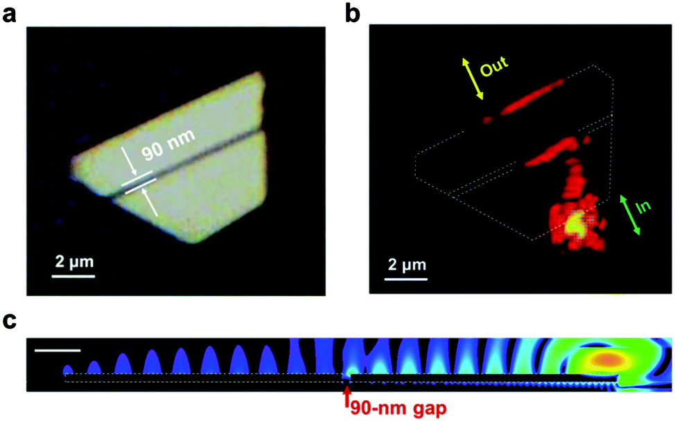 | ||
| Fig. 5 (a) Optical image of a Ag nanoplate involving a 90 nm wide gap fabricated by FIB milling. (b) The observed radiation distribution with two bright scattering areas at the nanogap and the output antenna side. The radiation at the side opposite to the input side clearly demonstrates that SPPs are efficiently tunneling through the nano-gap. (c) The calculated electric field intensity distribution of SPPs propagating on the nanoplate surface and tunnelling through a 90 nm wide gap (scale bar is 1 μm). | ||
Tunnelling and scattering of SPP evanescent fields are very sensitive to the change in the optical properties of materials inside the gap.45 We note that the nano-gap can contain various biochemical nano-materials inside, of which response can be monitored via SPPs tunnelling through the nano-gap. Furthermore, the SPPs can excite fluorescence or Raman scattering of nano-scale materials inside the nano-gap with very high efficiency, since the evanescent fields of SPPs are readily condensed down to the sub-wavelength scale. Here, output signals from the target materials can be well separated from the incident light by means of SPPs mediating the activation area (such as the nano-gap) and the input antenna side remotely. This separation can significantly improve the signal qualities of spectroscopic measurements by excluding the noise from the stray incident light.
The surface of our Ag nanoplates is ultraclean and has no surfactant, while that of the solution-grown Ag nanoplates is covered by the surfactant. Such a clean surface is quite important for further surface modification after synthesis. Furthermore, our Ag nanoplates are much larger (∼50 μm) than those typically synthesized by the solution growth method (<5 μm).
4. Conclusions
The nanoplasmonic platform made of a single-crystal Ag nanoplate demonstrates that it can naturally merge optical nano-antennas and surface plasmonic evanescent field playgrounds on a system. The atomically flat surface and crystallographic side facets of the Ag nanoplate allow superior qualities for SPP manipulation and plasmonic antenna operation by minimizing random scattering and dephasing of surface plasmons. Furthermore, the well-defined crystal geometry enables highly precise alignment of the plasmonic elements and their reliable operations as desired and predicted theoretically. The unique nano-optical performances are fully reproduced and analyzed through numerical FDTD simulations. We expect that the converged nanoplasmonic platform may be employed for diverse physical and biochemical applications such as SPR biochemical sensors, fluorescence-based spectroscopic measurements, near-field optical lab-on-a-chip, and even plasmonic nano-circuitry.Acknowledgements
M.-K.S. acknowledges support of this work by Basic Science Research Program (2011-0015119 and 2013R1A2A2A01014224) of NRF and HRHRP of KAIST. B.K. acknowledges support of this work by Korean Health Technology R&D Project (A121983), Ministry of Health & Welfare, Korea. TEM analysis was performed at the KBSI in Daejeon.Notes and references
- C. A. Balancis, Antenna Theory: Analysis and Design, Wiley, New York, 2005 Search PubMed.
- P. Muhlschlegel, H. J. Eisler, O. J. F. Martin, B. Hecht and D. W. Pohl, Science, 2005, 308, 1607–1609 CrossRef CAS PubMed.
- S. A. Maier, Plasmonics: Fundamentals and Applications, Springer, 2007 Search PubMed.
- J. A. Schuller, E. S. Barnard, W. S. Cai, Y. C. Jun, J. S. White and M. L. Brongersma, Nat. Mater., 2010, 9, 193–204 CrossRef CAS PubMed.
- L. Novotny and N. van Hulst, Nat. Photonics, 2011, 5, 83–90 CrossRef CAS.
- S. Kuhn, U. Hakanson, L. Rogobete and V. Sandoghdar, Phys. Rev. Lett., 2006, 97, 017402–017405 CrossRef.
- F. Tam, G. P. Goodrich, B. R. Johnson and N. J. Halas, Nano Lett., 2007, 7, 496–501 CrossRef CAS PubMed.
- J. N. Anker, W. P. Hall, O. Lyandres, N. C. Shah, J. Zhao and R. P. Van Duyne, Nat. Mater., 2008, 7, 442–453 CrossRef CAS PubMed.
- T. H. Taminiau, F. D. Stefani, F. B. Segerink and N. F. Van Hulst, Nat. Photon., 2008, 2, 234–237 CrossRef CAS.
- J. N. Farahani, D. W. Pohl, H. J. Eisler and B. Hecht, Phys. Rev. Lett., 2005, 95, 017402–017405 CrossRef CAS.
- W. S. Cai, A. P. Vasudev and M. L. Brongersma, Science, 2011, 333, 1720–1723 CrossRef CAS PubMed.
- K. C. Y. Huang, Y. C. Jun, M. K. Seo and M. L. Brongersma, Opt. Express, 2011, 19, 19084–19092 CrossRef PubMed.
- A. Kinkhabwala, Z. F. Yu, S. H. Fan, Y. Avlasevich, K. Mullen and W. E. Moerner, Nat. Photonics, 2009, 3, 654–657 CrossRef CAS.
- A. G. Curto, G. Volpe, T. H. Taminiau, M. P. Kreuzer, R. Quidant and N. F. van Hulst, Science, 2010, 329, 930–933 CrossRef CAS PubMed.
- Y. C. Jun, K. C. Y. Huang and M. L. Brongersma, Nat. Commun., 2011, 2, 283–288 CrossRef PubMed.
- S.-H. Kwon, J.-H. Kang, C. Seassal, S.-K. Kim, P. Regreny, Y.-H. Lee, C. M. Lieber and H.-G. Park, Nano Lett., 2010, 10, 3679–3683 CrossRef CAS PubMed.
- E. S. Barnard, R. A. Pala and M. L. Brongersma, Nat. Nanotechnol., 2011, 6, 588–593 CrossRef CAS PubMed.
- M. W. Knight, H. Sobhani, P. Nordlander and N. J. Halas, Science, 2011, 332, 702–704 CrossRef CAS PubMed.
- K. C. Y. Huang, M. K. Seo, Y. Huo, T. Sarmiento, J. S. Harris and M. L. Brongersma, Nat. Commun., 2012, 3, 1005–1010 CrossRef PubMed.
- H. Raether, Surface Plasmons on Smooth and Rough Surfaces and on Gratings, Springer-Verlag, Berlin, 1988 Search PubMed.
- J. Homola, S. S. Yeea and G. Gauglitzb, Sensors and Actuators B: Chemical., 1999, 54, 3–15 CrossRef CAS.
- G. Eda, G. Fanchini and M. Chhowalla, Nat. Nanotechnol., 2008, 3, 270–274 CrossRef CAS PubMed.
- D. Choi, D. Wang, I.-T. Bae, J. Xiao, Z. Nie, W. Wang, V. V. Viswanathan, Y. J. Lee, J.-G. Zhang, G. L. Graff, Z. Yang and J. Liu, Nano Lett., 2010, 10, 2799–2805 CrossRef CAS PubMed.
- Y. Wu, Z. Wen and J. Li, Adv. Mater., 2011, 23, 1126–1129 CrossRef CAS PubMed.
- J. Go, P. R. Nair, B. Reddy Jr, B. Dorvel, R. Bashir and M. A. Alam, ACS Nano, 2012, 6, 5972–5979 CrossRef CAS PubMed.
- K. A. Homan, M. Souza, R. Truby, G. P. Luke, C. Green, E. Vreeland and S. Emelianov, ACS Nano, 2012, 6, 641–650 CrossRef CAS PubMed.
- W. Dang, H. Peng, H. Li, P. Wang and Z. Liu, Nano Lett., 2010, 10, 2870–2876 CrossRef CAS PubMed.
- B. Nikoobakht and X. Li, ACS Nano, 2012, 6, 1883–1887 CrossRef CAS PubMed.
- F. Wang, J.-H. Seo, Z. Ma and X. Wang, ACS Nano, 2012, 6, 2602–2609 CrossRef CAS PubMed.
- J. S. Huang, V. Callegari, P. Geisler, C. Bruning, J. Kern, J. C. Prangsma, X. F. Wu, T. Feichtner, J. Ziegler, P. Weinmann, M. Kamp, A. Forchel, P. Biagioni, U. Sennhauser and B. Hecht, Nat. Commun., 2010, 1, 150–157 CrossRef PubMed.
- S. Viarbitskaya, A. Teulle, R. Marty, J. Sharma, C. Girard, A. Arbouet and E. Dujardin, Nat. Mater., 2013, 12, 426–432 CrossRef CAS PubMed.
- X.-Y. Zhang, T. Zhang, A. Hu, Y.-J. Song and W. W. Duley, Appl. Phys. Lett., 2012, 101, 153118–153121 CrossRef.
- X.-Y. Zhang, A. Hu, T. Zhang, W. Lei, X.-J. Xue, Y. Zhou and W. W. Duley, ACS Nano, 2011, 5, 9082–9092 CrossRef CAS PubMed.
- P. Nagpal, N. C. Lindquist, S. H. Oh and D. J. Norris, Science, 2009, 325, 594–597 CrossRef CAS PubMed.
- J. Park, P. Ambwani, M. Manno, N. C. Lindquist, P. Nagpal, S.-H. Oh, C. Leighton and D. J. Norris, Adv. Mater., 2012, 24, 3988–3992 CrossRef CAS PubMed.
- H. Ditlbacher, A. Hohenau, D. Wagner, U. Kreibig, M. Rogers, F. Hofer, F. R. Aussenegg and J. R. Krenn, Phys. Rev. Lett., 2005, 95, 257403–257406 CrossRef.
- T. Kang, W. Choi, I. Yoon, H. Lee, M. K. Seo, Q. H. Park and B. Kim, Nano Lett., 2012, 12, 2331–2336 CrossRef CAS PubMed.
- B. Prade, J. Y. Vinet and A. Mysyrowicz, Phys. Rev. B, 1991, 44, 13556–13572 CrossRef.
- A. Taflove and S. C. Hagness, Computational Electrodynamics: the finite-difference timedomain method, Artech House, Boston, 3rd edn, 2005 Search PubMed.
- H. L. Offerhaus, B. van den Bergen, M. Escalante, F. B. Segerink, J. P. Korterik and N. F. van Hulst, Nano Lett., 2005, 5, 2144–2148 CrossRef CAS PubMed.
- A. Bouhelier and G. P. Wiederrecht, Opt. Lett., 2005, 30, 884–886 CrossRef CAS.
- K. Demarest, Z. Huang and R. Plumb, IEEE Trans. Antennas Propag., 1996, 44, 1150–1157 CrossRef.
- Y. R. Fang, H. Wei, F. Hao, P. Nordlander and H. X. Xu, Nano Lett., 2009, 9, 2049–2053 CrossRef CAS PubMed.
- S. Lal, J. H. Hafner, N. J. Halas, S. Link and P. Nordlander, Acc. Chem. Res., 2012, 45, 1887–1895 CrossRef CAS PubMed.
- W. Bao, M. Melli, N. Caselli, F. Riboli, D. S. Wiersma, D. S. M. Staffaroni, H. Choo, D. F. Ogletree, S. Aloni, J. Bokor, S. Cabrini, F. Intonti, M. B. Salmeron, E. Yablonovitch, P. J. Schuck and A. Weber-Bargioni, Science, 2012, 338, 1317–1321 CrossRef CAS PubMed.
Footnotes |
| † Electronic supplementary information (ESI) available: Experimental details including synthesis of single-crystal Ag nanoplates, surface roughness and thickness of as-synthesized Ag nanoplates measured using an Atomic Force Microscope (AFM), simulation results of the coupling efficiency of incident light to SPPs at the antenna side and the transmission and reflection coefficients as a function of the gap width, and blockade of SPPs by a heavy scattering object placed on the nanoplate. See DOI: 10.1039/c3nr04492k |
| ‡ These authors contributed equally to this work. |
| This journal is © The Royal Society of Chemistry 2014 |