DOI:
10.1039/C3NR04341J
(Paper)
Nanoscale, 2014,
6, 449-456
Solvent-type-dependent polymorphism and charge transport in a long fused-ring organic semiconductor†
Received
15th August 2013
, Accepted 18th October 2013
First published on 22nd October 2013
Abstract
Crystalline polymorphism of organic semiconductors is among the critical factors in determining the structure and properties of the resultant organic electronic devices. Herein we report for the first time a solvent-type-dependent polymorphism of a long fused-ring organic semiconductor and its crucial effects on charge transport. A new polymorph of 5,11-bis(triethylsilylethynyl)anthradithiophene (TES ADT) is obtained using solvent-assisted crystallization, and the crystalline polymorphism of TES ADT thin films is correlated with their measured hole mobilities. The best-performing organic thin film transistors of the two TES ADT polymorphs show subthreshold slopes close to 1 V dec−1, and threshold voltages close to zero, indicating that the density of traps at the semiconductor–dielectric interface is negligible in these devices and the observed up to 10-fold differences in hole mobilities of devices fabricated with different solvents are largely resultant from the presence of two TES ADT polymorphs. Moreover, our results suggest that the best-performing TES ADT devices reported in the literature correspond to the new polymorph identified in this study, which involves crystallization from a weakly polar solvent (such as toluene and chloroform).
Introduction
Crystalline polymorphism is relevant to the physical properties of organic solids including pharmaceutical crystals, energetic materials, dyes, and organic semiconductors.1 This phenomenon is widely encountered in organic solids, mostly because their intermolecular interactions are weak, of van der Waals type. For organic semiconductors, polymorphism was shown to strongly affect long-range order,2 electron–phonon coupling,3,4 as well as band structures and charge transport.5 Previously reported polymorphic organic semiconductors include oligoacenes,6 oligothiophenes,7–9 tetracyanoquinodimethane (TCNQ),10 functionalized pentacene,11,12 dibenzo- or dithiophene-tetrathiafulvalene (DB-, or DT-TTF),4,13 and fluorinated anthradithiophene.14 So far the typical approaches used to manipulate polymorphs of organic semiconductors include heating,11,14,15 substrate confinement (thin film vs. bulk),16,17 substrate modification,18 deposition temperature control,7,19 pressure,20 and solution shear.12 Solvent-dependent polymorphism has been previously reported in single crystals of DB-TTF and DT-TTF with short (2) fused rings due to their backbone (π–π) and S⋯S interactions.4,13 In addition, single crystals of non-fused ring didodecyl-quarterthiophenes exhibit polymorphs induced by the conformational changes of their pedant side groups during crystallization from good or poor solvents.9 To the best of our knowledge, solvent-dependent polymorphism of a linear, long fused ring organic semiconductor (n > 4) has not been reported, although conjugated molecules with 4 or more fused rings represent an extremely important class of high performance organic semiconductors.
5,11-Bis(triethylsilylethynyl)anthradithiophene (TES ADT) is a solution-processable, high-performance small molecule organic semiconductor with five fused rings, showing hole mobilities as high as 1 cm2 V−1 s−1.21 However, the reproducibility of devices fabricated with this material spans three to four orders of magnitude in transistors fabricated by various methods, such as spin-coating coupled with solvent vapor annealing22–24 or aging,25 drop casting,26–28 and blending with polymers to form vertically phase separated semiconductor–dielectric structures.29Table 1 lists some representative mobility values reported in the literature for TES ADT based organic thin film transistors (OTFTs), along with their solvent choices and process conditions. As we demonstrate in this work, a solvent-type-dependent polymorphism can contribute significantly to this large spread in TES ADT device performance. The reported bulk TES ADT crystal has a triclinic unit cell with parameters of a = 6.9107 Å, b = 7.4163 Å, c = 16.7167 Å, α = 96.4022°, β = 92.0203°, and γ = 106.0026° (cell volume V = 816.47 Å3).21,30 Herein we show that this is not the only crystalline packing that TES ADT can display when processed at room temperature, and that the observed polymorphism critically affects device performance, changing the maximum mobility by up to 10 times under the same testing conditions. Moreover, our results suggest that the highest-performing TES ADT devices reported in the literature21,23,27,28 correspond to the new polymorph identified in this study (instead of the well-known triclinic-type bulk unit cell), which involves slow solution crystallization processes using a weakly polar solvent (such as toluene and chloroform). In this study, we demonstrate solvent-dependent polymorphism of TES ADT (and long fused-ring organic semiconductor), by using solvent-assisted crystallization (SAC), which was proven to be a simple yet powerful method to fabricate high-quality crystalline thin films of functionalized heteroacenes including fluorinated TES ADT.32
Table 1 Previously reported hole mobility values of TES ADT-based OTFTs along with the corresponding solution process conditions, solvent choice, and dipole moments31 of the chosen solvents
| Mobility (cm2 V−1 s−1) |
Solvent (dipole moment) |
Process conditions |
Reference |
| 1.0 |
Toluene (0.375 D) |
Solution cast with a blade (1–2 wt%) |
Payne et al., 2005 (ref. 21) |
| 0.11 |
1,2-Dichloroethane (1.48 D) |
Solvent vapor annealing |
Dickey et al., 2006 (ref. 24) |
| 0.05 |
Toluene (0.375 D) |
Solvent vapor annealing |
Dickey et al., 2006 (ref. 24) |
| 0.02 |
THF (1.75 D) |
Solvent vapor annealing |
Dickey et al., 2006 (ref. 24) |
| 0.01 |
Acetone (2.88 D) |
Solvent vapor annealing |
Dickey et al., 2006 (ref. 24) |
| 0.002 |
Hexane (0 D) |
Solvent vapor annealing |
Dickey et al., 2006 (ref. 24) |
| 0.43 |
Chloroform (1.04 D) |
Solvent vapor annealing |
Lee et al., 2007 (ref. 23) |
| 0.42 |
Chloroform (1.04 D) |
Solution cast at 5 °C (4 wt%) |
Yu et al., 2011 (ref. 27) |
| 0.38–0.40 |
Toluene (0.375 D) |
Drop cast on Mylar (8 wt%) |
Yi et al., 2012 (ref. 28) |
Experimental section
Materials
TES ADT is synthesized based on a previously published procedure.21 Anhydrous toluene, chloroform, and THF are purchased from Sigma-Aldrich and EMD Millipore.
Film formation
TES ADT powder is dissolved in anhydrous solvent at a total solid concentration of 0.2 wt%. Drop casting of TES ADT solution is performed in a solvent–vapor-rich glass Petri dish with cover under ambient conditions.
TEM, electron diffraction and simulation
Electron diffraction and bright-field TEM are conducted with a Zeiss Libra 120 at 120 kV with an in-column energy filter. Electron diffraction experiments are conducted with an emission current as small as 5 × 10⁻⁶ A and a 1-micron-diameter selected area aperture. The Al (111) (0.234 nm) ring is used to calibrate all electron diffraction patterns. WebEMAPS (http://emaps.mrl.uiuc.edu) and Mercury2.3 (www.ccdc.cam.ac.uk/mercury/) are used to simulate electron diffraction patterns and unit cell views.
Organic thin film transistors
The substrates used for OTFT fabrication consist of highly doped Si gate electrodes with thermally grown SiO2 gate dielectrics and Ti/Au source and drain contacts defined by photolithography and deposited by e-beam evaporation. These substrates are sequentially cleaned in heated baths of acetone and then isopropyl alcohol, followed by exposure to UV/ozone, each for 10 minutes. The substrates were treated with phenyltrichlorosilane (PTS) and/or a pentafluorobenzenethiol (PFBT). The details of the phenyltrichlorosilane (PTS) treatment on wafer substrates are available elsewhere.12 For PFBT treatment, they are placed in individual solutions of 30 mM PFBT in ethanol and left undisturbed for 30 minutes.33 They are removed from solution, rinsed in ethanol, and further sonicated in ethanol for 5 minutes and dried with nitrogen. The substrate is placed in a Petri dish and a TES ADT solution (0.2% in room-temperature toluene or THF) is deposited by drop casting. Extra solvent is syringed around the substrate and a cover is placed over the Petri dish to keep the solution and substrate in a solvent-rich environment while the film crystallizes.32 The devices are measured using an Agilent 4155C Semiconductor Parameter Analyzer connected to a probe station. The transistor active layers are also used in GIXRD experiments (Philips X'Pert).
UV-Vis absorption and simulation
Experimental UV-Vis spectra are obtained on TES ADT thin films crystallized on a quartz substrate under conditions consistent with the ones fabricated as OTFT active layers. The theoretical UV-Vis spectrum is calculated for a one-molecular-layer film constructed based on the bulk unit cell structure at the level of time-dependent density funcitonal theory (TDDFT) with the adiabatic local density approximation (ALDA) approximation using the Yambo code. (Details and references are available in the ESI.†) Sixty valence bands and sixty conduction bands around the Fermi level were correlated in the calculation. The local field effects were considered by setting the dimension of the response function to 300 to account for the charge oscillations induced by the external potential. The dimension of the exchange-correlation kernel was set to be equal to that of the response function size.
Results and discussion
Fig. 1a and b show the molecular structure of TES ADT and a unit cell view of bulk TES ADT. Fig. 1c and d show representative optical micrographs of the resultant TES ADT films with toluene and tetrahydrofuran (THF) as the solvents, respectively. In Fig. 1e, a calculated UV-Vis spectrum for a TES ADT thin film constructed based on the bulk unit cell structure using TDDFT is compared with the experimental results. A close match between the simulation and experimental spectra is obtained. Experimental UV-Vis spectra of SAC fabricated TES ADT films yield an optical absorption onset of 614 nm (2.02 eV) for films from THF solution, and 643 nm (1.93 eV) for films from toluene solution (Fig. 1e). Fig. 2a presents the grazing-incidence X-ray diffraction (GIXRD) results of TES ADT films fabricated from THF, chloroform, and toluene solutions. TES ADT films fabricated from both THF and toluene solutions are highly crystalline as evidenced by their strong diffraction peak intensities. Both films have dominating (00l) type reflections, which indicate that the TES ADT molecules are present on the substrate with the bulky side group touching down (Fig. 2b). Fig. 2b provides a simulated side view of TES ADT films on the substrate down the “a” axis using their bulk unit cell. However, the (001) reflection in the film produced from the toluene solution (1.630 nm) is slightly smaller than that from THF (1.637 nm), indicating only a very small difference (<0.5%) in their “c” value.
 |
| | Fig. 1 Molecular structure (a) and a unit cell view of TES ADT down the “b” axis in its bulk phase (b). Optical micrographs of TES ADT films prepared from SAC are shown in (c) and (d), with toluene and THF solvents, respectively. (e) Experimental and calculated UV-Vis spectra of TES ADT thin films. The theoretical UV-Vis spectrum is calculated for a one-molecular-layer film constructed based on the bulk unit cell structure at the level of time-dependent DFT (TDDFT) with the adiabatic local density approximation (ALDA) (details in the Experimental section and ESI†). | |
 |
| | Fig. 2 (a) GIXRD of TES ADT thin films slowly crystallized from chloroform, THF and toluene solutions by the SAC approach in a solvent-rich environment. The films from chloroform and toluene share the same (001) d-spacing of 1.630 nm, which is slightly smaller than that of the TES ADT films from THF solution (1.637 nm). (b) A unit cell view of TES ADT films on the substrate based on its bulk unit cell. The discussion on TES ADT films from chloroform solution is given later in the text after the detailed comparison between the films from THF and toluene solutions. | |
SAED patterns of TES ADT films from THF solution match well with a simulated [001] zone diffraction pattern of TES ADT's triclinic, bulk unit cell21 as shown in Fig. S1,† suggesting that the TES ADT films fabricated by the SAC approach from THF solution consistently yield the previously reported triclinic polymorph of TES ADT with little mixed crystal structures. (Additional four representative experimental patterns are given in Fig. S2,† all in agreement with this result.) These SAED patterns correspond to an angle of 73 ± 1° between a* and b* (γTHF = 107 ± 1°), aTHF = 0.67 ± 0.01 nm and bTHF = 0.72 ± 0.01 nm (the average and standard deviation are based on measurements from 5 or more diffraction patterns), very similar to its bulk unit cell parameters (106°, 0.69 nm, and 0.74 nm, respectively). For convenience, we name the unit cell corresponding to the thin films grown from THF solution as the “α phase”. A comparison of the typical bright-field TEM and SAED patterns of THF- and toluene-solution crystallized TES ADT films is shown in Fig. 3, both in their [001] zone. The SAED pattern of the TES ADT film fabricated from the toluene solution (Fig. 3d) is distinctively different from the α phase pattern, both in terms of a and b values as well as the angle between a* and b*. The a and b values of the TES ADT film crystallized from toluene solution are respectively aToluene = 1.85 ± 0.03 nm and bToluene = 2.22 ± 0.02 nm. The measured γToluene = 90 ± 1°, and as we mentioned earlier, the GIXRD results suggest cToluene ≈ cTHF. This new unit cell structure has not been previously reported and we name it the “β phase”. Four additional, representative SAED patterns of TES ADT films crystallized from toluene solution are shown in Fig. S3,† suggesting highly consistent results on the crystalline polymorph identification. In Fig. 3c, a simplified unit cell is drawn to illustrate the ADT backbone position in the bulk unit cell down the c axis. In comparison, Fig. 3f has a to-scale “β phase” unit cell view, highlighting the change in lattice geometry. (The details of the molecular arrangement inside the unit cell are still under investigation.) The TES ADT (001) plane area changes from 0.46 nm2 in the α phase to 4.11 nm2 in the β phase by a factor of 8.93. Because the change in the packing efficiency and cell volume of polymorphs of organic crystals, organic semiconductors, and especially long fused-ring semiconductors are often small,2,11,14,34 even under shear12 or pressure20 (<5%), this implies that there are 9 TES ADT molecules per unit cell (Z = 9) in the β phase, considering that the c value is almost unchanged (<0.5% according to our GIXRD data). Table 2 compares the bulk and thin film phases of TES ADT including their lattice parameters and process conditions.
 |
| | Fig. 3 Experimental [001] zone SAED patterns (a and d), bright-field TEM (b and e), and simplified, to-scale unit cell views (c and f) of SAC fabricated TES ADT films, in the “α phase” crystallized from THF solution (a–c) and in the “β phase” crystallized from toluene solution (d–f). The details of the molecular arrangement inside the “β phase” unit cell are still under investigation. The yellow circles in the bright-field TEM images highlight the selected area diffraction aperture. | |
Table 2 A summary of TES ADT unit cell structures and fabrication conditions
|
|
Bulk (α phase)21 |
Thin film α phase |
Thin film β phase |
|
a
|
0.69 nm |
0.67 nm |
1.85 nm |
|
b
|
0.74 nm |
0.72 nm |
2.22 nm |
|
c
|
1.66 nm |
1.67 nm |
1.67 nm |
|
α
|
96° |
— |
— |
|
β
|
92° |
— |
— |
|
γ
|
106° |
107° |
90° |
|
Z
|
1 |
1 |
9 |
|
A
(001)
|
0.49 nm2 |
0.46 nm2 |
4.11 nm2 |
| Fabrication conditions |
Solution-grown single crystals |
Thin films by SAC (0.2 wt% in THF) |
Thin films by SAC (0.2 wt% in toluene or chloroform) |
To evaluate the polymorphism effect on charge transport, OTFTs are fabricated on heavily doped (n-type) silicon substrates with 200 nm thermal oxide as the insulator, and Ti/Au bottom contacts as source and drain electrodes. Devices with PFBT treated contacts,33 PTS treated oxide,12 and a combination of both treatments were fabricated and characterized from TES ADT thin films deposited from toluene and THF by the SAC approach. Unfortunately, the devices fabricated from toluene on PTS treated SiO2 did not show uniform films as a result of the very low surface energy and thus we could not estimate the mobility. TES ADT based OTFTs with PFBT treatment yielded an average mobility μToluene = 0.12 ± 0.07 cm2 V−1 s−1 for devices deposited from toluene and μTHF = 9.7 × 10⁻³ ± 0.002 cm2 V−1 s−1 for the ones fabricated using THF solutions (each average is obtained from 10 devices; Table 3). Similarly, for PFBT/PTS treatment, the resulting average mobilities are μToluene = 0.22 ± 0.03 cm2 V−1 s−1 and μTHF = 0.06 ± 0.01 cm2 V−1 s−1, respectively (each average is obtained from 10 devices; Table 3). Fig. 4 and 5 show typical transfer and output characteristics of THF and toluene solution crystallized, bottom-contact OTFT devices of similar channel lengths, measured at room-temperature, in a vacuum. Although device properties did vary slightly as a result of the surface treatment, for all cases the results consistently showed superior mobilities for the TES ADT films crystallized from toluene solution. The mobility values were estimated from the slope of the transfer curve in the saturation regime (VDS = −40 V) (Fig. 4a and 5a) using the following expression:
| |  | (1) |
where
L is the channel length,
W the channel width, and
ci the capacitance per unit area of the dielectric (17.3 nF cm
−2 for 200 nm thick SiO
2). These plots yield a mobility
μ = 0.36 cm
2 V
−1 s
−1 for the toluene device (
Fig. 4) and
μ = 0.06 cm
2 V
−1 s
−1 for the THF device (
Fig. 5). The drain currents (
ID) at low drain–source voltages in the transport graphs (
Fig. 4b and
5b) are linear, pointing to the fact that the contact resistance, while not negligible, is small and thus not critical in the evaluation of electrical properties in these cases. Furthermore, these devices have subthreshold slopes close to 1 V dec
−1, and threshold voltages close to zero (
Vth = 0.57 V for the toluene device and −0.14 V for the devices from THF solution), indicating that the density of traps at the semiconductor–dielectric interface is nearly the same, and very small.
35 These observations are important, as they suggest that the observed large differences are not attributed to traps or contact effects, which can result in imperfections in the device operation, but they indeed largely originate from the intrinsic structure and properties of the active layers in the transistor channel, as a result of the presence of two polymorphs.
Table 3 A summary of OTFT device performance of TES ADT thin films fabricated by SAC from 0.2 wt% solutions with the PFBT treated electrode and PTS treated substrate (average and standard deviation are obtained from 10 devices in each case)
| Solvent |
Thin film polymorph |
Mobility μ on PFBT/PTS (cm2 V−1 s−1) |
Mobility μ on PFBT (cm2 V−1 s−1) |
| Toluene |
β phase |
0.22 ± 0.03 |
0.12 ± 0.07 |
| THF |
α phase |
0.06 ± 0.01 |
9.7 × 10⁻³ ± 0.002 |
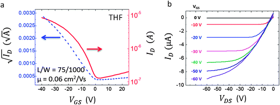 |
| | Fig. 4 Representative transfer (a) and output characteristics (b) for THF solution crystallized TES ADT films. For the transfer characteristics, a source–drain voltage VDS = −40 V was used. The device shown in this plot has a channel width W of 1000 μm and channel length L of 75 μm. | |
 |
| | Fig. 5 Representative transfer (a) and output characteristics (b) for toluene solution crystallized TES ADT films. For the transfer characteristics, a source–drain voltage VDS = −40 V was used. The device shown in this plot has a channel width W of 56 μm and channel length L of 100 μm. | |
To explore if the large difference in the solvent boiling point is responsible for the observed TES ADT polymorphism (the boiling point of toluene is 110.6 °C and THF 66 °C), we also investigated the crystal structure of thin films deposited from chloroform solutions (the boiling point of chloroform is 61.2 °C). Representative TEM and SAED patterns of chloroform solution crystallized TES ADT films are presented in Fig. 6, showing lattice parameters of a = 1.88 ± 0.01 nm, b = 2.20 ± 0.01 nm, and γ = 90 ± 1°, which are consistent with those of the “β phase”. In addition, according to the GIXRD results (Fig. 2), TES ADT films grown from chloroform solution have a (001) refection corresponding to 1.630 nm, identical to the one from the toluene solution (“β phase”), but smaller than that from the THF solution (1.637 nm).
 |
| | Fig. 6 SAED patterns (top row) and corresponding bright-field TEM images (bottom row) of the TES ADT films grown from chloroform solution, consistently demonstrating a 90 degree angle between a* and b*, as well as other features that match up with the “β phase”. The yellow circles in the bright-field TEM images highlight the selected area diffraction aperture. | |
Instead of boiling point, polarity (dipole moment) of the solvent choice seems to strongly correlate with the observed polymorphism and device performance. From our own results and the ones from the literature (Table 1), it is clear that a strongly polar solvent (such as THF, with a dipole moment of 1.75 D) promotes the “α phase” (triclinic bulk polymorph), which corresponds to lower mobilities (≤0.02 cm2 V−1 s−1), while weakly polar solvents (such as toluene and chloroform with dipole moments of 0.375 D and 1.04 D, respectively) yield the “β phase”, which is responsible for the highest-performing devices of TES ADT thin films (up to 0.3–1 cm2 V−1 s−1).21,23,27,28 TES ADT films grown from dilute hexane solution demonstrate “β phase” unit cell according to their SAED patterns (Fig. S5†), suggesting that the nonpolar solvent also promote the newly discovered polymorph.
The optical micrograph of the room temperature “SAC fabricated” TES ADT films from chloroform (Fig. S4†) shows large voids between their fractal-shaped crystalline domains, which prevents us from obtaining meaningful charge transport results to compare with the other two solvents. However, it is noticeable that Yu et al.27 performed low-temperature solution casting of highly concentrated (4 wt%) TES ADT/chloroform solution to overcome this issue and achieved hole mobilities as high as 0.4 cm2 V−1 s−1. Lee et al.23 used chloroform as a vapor source in solvent vapor annealing of TES ADT films, reporting remarkable mobilities also reaching 0.4 cm2 V−1 s−1. With high concentration toluene solutions (up to 2 or 8 wt%), Payne et al.21 reported mobilities up to 1 cm2 V−1 s−1 for blade cast TES ADT films, and Yi et al.28 obtained mobilities of 0.38–0.40 cm2 V−1 s−1 from drop cast TES ADT films on a plastic substrate (Mylar). Similarly, our results in this work yield mobilities as high as 0.36 cm2 V−1 s−1 for SAC fabricated TES ADT films from dilute (0.2 wt%) toluene solution. These agree well with the fact that both chloroform and toluene (dipole moments of 0.4–1 D) promote the “β phase” of the TES ADT. The lattice unit cells and crystal structures of small molecule organic crystals are strongly coupled with their film morphologies, as it was previously shown in studies carried out on a variety of organic semiconductors.1–19,32,37,38 Indeed, the photos taken on SAC-fabricated bottom contacts and bottom gate TES ADT thin film transistors shown in Fig. 1c and d disclose long, thin needles in films obtained from toluene and a more granular structure for the THF films. The devices presented in this study consist of similar channel lengths to minimize the effect of the film microstructure. Nevertheless, the resulting electrical properties arise from the cumulative structure and morphology effects originating from the presence of the two polymorphs in this material. In addition, the existence of mixed phases cannot be ruled out. The asymmetric shape of (001) peaks in Fig. 2 and the occasionally observed GIXRD peak splitting in some of the films may indicate a change in ratios of mixed phases. Mixed phases may not be captured in the SAED patterns since SAED tends to probe local structures (at a micron scale).
A recent work of Stingelin et al.,39 highlighted temperature-driven polymorphs of TES ADT films. The triclinic thin film α phase has a calculated average π–π distance of 3.38 Å and π–π overlap slippage of 1.73 and 3.08 Å.39 The single crystal α phase has an average π–π distance of 3.26 Å and π–π overlap slippage of 1.84 and 3.23 Å.39 It is well known that the π–π distance and π–π overlap greatly affect charge transport of organic semiconductors, such as functionalized pentacene.12 However, because the detailed atomic positions of the newly discovered polymorph are not yet fully resolved based on the available X-ray and electron diffraction, the role of the π–π distance and π–π overlap is undetermined in this work.
Surface energy and nucleation kinetics are decisive in determining the polymorphism and crystallization of crystals and especially molecular crystals.1,16,36 We believe that the solvent choice and specific intermolecular interactions between the solvent and aggregated clusters in the initial stage of crystallization cause the observed remarkable polymorphism during the solution crystallization of TES ADT. A well-known acene-based analog, 6,13-bis(triisopropylsilylethynyl)pentacene (TIPS pentacene), does not exhibit significant solvent-dependent polymorphism to the best of our knowledge. This suggests that S⋯S interactions may play an important role in the initial nucleation and final polymorph type of TES ADT, similar to the cases in tetrathiafulvalene.4,13
Conclusion
In summary, we report a solvent-type-dependent polymorphism of a long fused-ring organic semiconductor and its critical effects on charge transport for the first time. A new polymorph of TES ADT in thin films is identified and examined in detail with electron diffraction, grazing-incidence X-ray diffraction, UV-Vis, molecular simulation, and OTFT measurements. Since the density of traps at the semiconductor–dielectric interface is negligible in our best-performing TES ADT OTFTs, we largely attribute the observed up to 10-fold differences in the maximum mobilities of devices fabricated with different solvents to the intrinsic packing of the two resultant TES ADT polymorphs. In addition, the results from this work suggest that the highest-performing TES ADT devices reported in the literature correspond to the new polymorph identified in this study, which involves slow solution crystallization processes using a solvent with weak polarity (such as toluene and chloroform).
Acknowledgements
This research was conducted at the Center for Nanophase Materials Sciences, which is sponsored at Oak Ridge National Laboratory by the Scientific User Facilities Division, Office of Basic Energy Sciences, U.S. Department of Energy. The computational work used the resources of the National Energy Research Scientific Computing Center, which are supported by the Office of Science of the U.S. Department of Energy under Contract no. DE-AC02-05CH11231. JC appreciates a web-based electron diffraction simulation software developed in Prof. J. M. Zuo's lab (J.M. Zuo and J.C. Mabon, Web-based Electron Microscopy Application Software: Web-EMAPS, Microsc Microanal 10 (Suppl 2), 2004; URL: http://emaps.mrl.uiuc.edu/). D.L. acknowledges partial support from NSF under award #ECCS-1151140 and # EPS -1158862. The work at WFU is supported by the National Science Foundation (ECCS-1102275 and ECCS-1254757).
References
-
J. Bernstein, Polymorphism in Molecular Crystals, Oxford University Press, New York, 2002 Search PubMed.
- D. Fichou, J. Mater. Chem., 2000, 10, 571 RSC.
- A. Brillante, I. Bilotti, R. G. Della Valle, E. Venuti and A. Girlando, CrystEngComm, 2008, 10, 923 RSC.
- A. Brillante, I. Bilotti, R. Della Valle, E. Venuti, S. Milita, C. Dionigi, F. Borgatti, A. Lazar, F. Biscarini, M. Mas-Torrent, N. Oxtoby, N. Crivillers, J. Veciana, C. Rovira, M. Leufgen, G. Schmidt and L. Molenkamp, CrystEngComm, 2008, 10, 1899 RSC.
-
(a) A. Troisi and G. Orlandi, J. Phys. Chem. B, 2005, 109, 1849 CrossRef CAS PubMed;
(b) V. Coropceanu, J. Cornil, D. A. da Silva, Y. Olivier, R. Silbey and J. L. Bredas, Chem. Rev., 2007, 107, 926 CrossRef CAS PubMed;
(c) M. Mas-Torrent and C. Rovira, Chem. Rev., 2011, 111, 4833 CrossRef CAS PubMed.
-
(a) T. Siegrist, C. Kloc, J. H. Schon, B. Batlogg, R. C. Haddon, S. Berg and G. A. Thomas, Angew. Chem., Int. Ed., 2001, 40, 1732 CrossRef CAS;
(b) C. C. Mattheus, A. B. Dros, J. Baas, A. Meetsma, J. L. de Boer and T. T. M. Palstra, Acta Crystallogr., Sect. C, 2001, 57, 939 CAS.
- L. Antolini, G. Horowitz, F. Kouki and F. Garnier, Adv. Mater., 1998, 10, 382 CrossRef CAS.
-
(a) A. Brillante, I. Bilotti, F. Biscarini, R. G. Della Valle and E. Venuti, Chem. Phys., 2006, 328, 125 CrossRef CAS PubMed;
(b) M. Campione, S. Tavazzi, M. Moret and W. Porzio, J. Appl. Phys., 2007, 101, 083512 CrossRef;
(c) P. Hermet, J. L. Bantignies, A. Rahmani, J. L. Sauvajol and M. R. Johnson, J. Phys. Chem. A, 2005, 109, 4202 CrossRef CAS PubMed.
- H. Pan, P. Liu, Y. Li, Y. Wu, B. Ong, S. Zhu and G. Xu, Adv. Mater., 2007, 19, 3240 CrossRef CAS.
- C. Avendano, Z. Zhang, A. Ota, H. Zhao and K. R. Dunbar, Angew. Chem., Int. Ed., 2011, 50, 6543 CrossRef CAS PubMed.
- J. Chen, J. Anthony and D. C. Martin, J. Phys. Chem. B, 2006, 110, 16397 CrossRef CAS PubMed.
- G. Giri, E. Verploegen, S. C. B. Mannsfeld, S. Atahan-Evrenk, D. H. Kim, S. Y. Lee, H. A. Becerril, A. Aspuru-Guzik, M. F. Toney and Z. Bao, Nature, 2011, 480, 504 CrossRef CAS PubMed.
- R. Pfattner, M. Mas-Torrent, I. Bilotti, A. Brillante, S. Milita, F. Liscio, F. Biscarini, T. Marszalek, J. Ulanski, A. Nosal, M. Gazicki-Lipman, M. Leufgen, G. Schmidt, L. W. Molenkamp, V. Laukhin, J. Veciana and C. Rovira, Adv. Mater., 2010, 22, 4198 CrossRef CAS PubMed.
- O. D. Jurchescu, D. A. Mourey, S. Subramanian, S. R. Parkin, B. M. Vogel, J. E. Anthony, T. N. Jackson and D. J. Gundlach, Phys. Rev. B: Condens. Matter Mater. Phys., 2009, 80, 085201 CrossRef.
- F. Lincker, A.-J. Attias, F. Mathevet, B. Heinrich, B. Donnio, J.-L. Fave, P. Rannou and R. Demadrille, Chem. Commun., 2012, 48, 3209 RSC.
- L. F. Drummy and D. C. Martin, Adv. Mater., 2005, 17, 903 CrossRef CAS.
- R. Ruiz, A. C. Mayer, G. G. Malliaras, B. Nickel, G. Scoles, A. Kazimirov, H. Kim, R. L. Headrick and Z. Islam, Appl. Phys. Lett., 2004, 85, 4926 CrossRef CAS.
- W.-Y. Chou, M.-H. Chang, H.-L. Cheng, Y.-C. Lee, C.-C. Chang and H.-S. Sheu, J. Phys. Chem. C, 2012, 116, 8619 CAS.
- C. C. Mattheus, A. B. Dros, J. Baas, G. T. Oostergetel, A. Meetsma, J. L. de Boer and T. T. M. Palstra, Synth. Met., 2003, 138, 475 CrossRef CAS.
- L. Farina, A. Brillante, R. G. Della Valle, E. Venuti, M. Amboage and K. Syassen, Chem. Phys. Lett., 2003, 375, 490 CrossRef CAS.
- M. M. Payne, S. R. Parkin, J. E. Anthony, C. C. Kuo and T. N. Jackson, J. Am. Chem. Soc., 2005, 127, 4986 CrossRef CAS PubMed.
- C.-H. Wang, Y.-C. Cheng, J.-W. Su, L.-J. Fan, P.-Y. Huang, M.-C. Chen and Y.-W. Yang, Org. Electron., 2010, 11, 1947 CrossRef CAS PubMed.
- W. H. Lee, D. H. Kim, J. H. Cho, Y. Jang, J. A. Lim, D. Kwak and K. Cho, Appl. Phys. Lett., 2007, 91, 092105 CrossRef.
- K. C. Dickey, J. E. Anthony and Y.-L. Loo, Adv. Mater., 2006, 18, 1721 CrossRef CAS.
- W. H. Lee, J. A. Lim, D. H. Kim, J. H. Cho, Y. Jang, Y. H. Kim, J. I. Han and K. Cho, Adv. Funct. Mater., 2008, 18, 560 CrossRef.
- C. S. Kim, S. Lee, E. D. Gomez, J. E. Anthony and Y.-L. Loo, Appl. Phys. Lett., 2008, 93, 103302 CrossRef.
- L. Yu, X. Li, E. Pavlica, M. A. Loth, J. E. Anthony, G. Bratina, C. Kjellander, G. Gelinck and N. Stingelin, Appl. Phys. Lett., 2011, 99, 263304 CrossRef.
- H. T. Yi, M. M. Payne, J. E. Anthony and V. Podzorov, Nat. Commun., 2012, 3, 1259 CrossRef PubMed.
-
(a) W. H. Lee, J. A. Lim, D. Kwak, J. H. Cho, H. S. Lee, H. H. Choi and K. Cho, Adv. Mater., 2009, 21, 4243 CrossRef CAS;
(b) Y. S. Chung, N. Shin, J. Kang, Y. Jo, V. M. Prabhu, S. K. Satija, R. J. Kline, D. M. DeLongchamp, M. F. Toney, M. A. Loth, B. Purushothaman, J. E. Anthony and D. Y. Yoon, J. Am. Chem. Soc., 2011, 133, 412 CrossRef CAS PubMed.
- S. S. Lee, C. S. Kim, E. D. Gomez, B. Purushothaman, M. F. Toney, C. Wang, A. Hexemer, J. E. Anthony and Y.-L. Loo, Adv. Mater., 2009, 21, 3605 CrossRef CAS.
-
J. A. Dean, Lange's Handbook of Chemistry, McGraw-Hill, Inc., 1998 Search PubMed.
- K. P. Goetz, Z. Li, J. W. Ward, C. Bougher, J. Rivnay, J. Smith, B. Conrad, S. Parkin, T. Anthopoulos, A. Salleo, J. E. Anthony and O. D. Jurchescu, Adv. Mater., 2011, 23, 3698 CrossRef CAS PubMed.
- J. W. Ward, M. A. Loth, R. J. Kline, M. Coll, C. Ocal, J. E. Anthony and O. D. Jurchescu, J. Mater. Chem., 2012, 22, 19047 RSC.
-
(a) C. P. Price, A. L. Grzesiak and A. J. Matzger, J. Am. Chem. Soc., 2005, 127, 5512 CrossRef CAS PubMed;
(b) T. Kakudate, N. Yoshimoto and Y. Saito, Appl. Phys. Lett., 2007, 90, 081903 CrossRef.
- H. Klauk, Chem. Soc. Rev., 2010, 39, 2643 RSC.
-
(a) J. M. McHale, A. Auroux, A. J. Perrotta and A. Navrotsky, Science, 1997, 277, 788 CrossRef CAS;
(b) M. Lang, A. L. Grzesiak and A. J. Matzger, J. Am. Chem. Soc., 2002, 124, 14834 CrossRef CAS PubMed.
- J. E. Anthony, S. Subramanian, S. R. Parkin, S. K. Park and T. N. Jackson, J. Mater. Chem., 2009, 19, 7984–7989 RSC.
- J. Chen, S. Subramanian, S. R. Parkin, M. Siegler, K. Gallup, C. Haughn, D. C. Martin and J. E. Anthony, J. Mater. Chem., 2008, 18, 1961 RSC.
- L. Yu, X. Li, E. Pavlica, F. P. V. Koch, G. Portale, I. da Silva, M. A. Loth, J. E. Anthony, P. Smith, G. Bratina, B. K. C. Kjellander, C. W. M. Bastiaansen, D. J. Broer, G. H. Gelinck and N. Stingelin, Chem. Mater., 2013, 25, 1823–1828 CrossRef CAS.
Footnote |
| † Electronic supplementary information (ESI) available. See DOI: 10.1039/c3nr04341j |
|
| This journal is © The Royal Society of Chemistry 2014 |
Click here to see how this site uses Cookies. View our privacy policy here. 


