Growth of linked silicon/carbon nanospheres on copper substrate as integrated electrodes for Li-ion batteries
Zailei
Zhang
a,
Yanhong
Wang
a,
Qiangqiang
Tan
*a,
Dan
Li
a,
Yunfa
Chen
a,
Ziyi
Zhong
b and
Fabing
Su
*a
aState Key Laboratory of Multiphase Complex Systems, Institute of Process Engineering, Chinese Academy of Sciences, Beijing, 100190, China. E-mail: qtan@mail.ipe.ac.cn; fbsu@mail.ipe.ac.cn; Fax: +86-10-82544851; Tel: +86-10-82544850
bInstitute of Chemical Engineering and Sciences, A*star, 1 Pesek Road, Jurong Island, 627833, Singapore
First published on 30th September 2013
Abstract
We report the growth of linked silicon/carbon (Si/C) nanospheres on Cu substrate as an integrated anode for Li-ion batteries. The Si/C nanospheres were synthesized by a catalytic chemical vapor deposition (CCVD) on Cu substrate as current collector using methyltrichlorosilane as precursor, a cheap by-product of the organosilane industry. The samples were characterized by X-ray diffraction, transmission electron microscopy, scanning electron microscopy, thermal gravimetry, Raman spectroscopy, nitrogen adsorption, inductively coupled plasma optical emission spectrometry, and X-ray photoelectron spectroscopy. It was found that the linked Si/C nanospheres with a diameter of 400–500 nm contain Si, CuxSi, and Cu nanocrystals, which are highly dispersed in the amorphous carbon nanospheres. A CCVD mechanism was tentatively proposed, in which the evaporated Cu atoms play a critical role to catalytically grown Si nanocrystals embedded within linked Si/C nanospheres. The electrochemical measurement shows that these Si/C nanospheres delivered a capacity of 998.9, 713.1, 320.6, and 817.8 mA h g−1 at 50, 200, 800, and 50 mA g−1 respectively after 50 cycles, much higher than that of commercial graphite anode. This is because the amorphous carbon, CuxSi, and Cu in the Si/C nanospheres could buffer the volume change of Si nanocrystals during the Li insertion and extraction reactions, thus hindering the cracking or crumbling of the electrode. Furthermore, the incorporation of conductive CuxSi and Cu nanocrystals and the integration of active electrode materials with Cu substrate may improve the electrical conductivity from the current collector to individual Si active particles, resulting in a remarkably enhanced reversible capacity and cycling stability. The work will be helpful in the fabrication of low cost binder-free Si/C anode materials for Li-ion batteries.
1. Introduction
Graphite materials, which have a theoretical specific capacity of 372 mA h g−1, are currently used as anode materials in commercial Li-ion batteries.1–3 However, a new generation of smaller and lighter portable electronic devices calls for new anode materials with higher lithium storage performance.4,5 Among the alternatives to the existing carbon-based anode materials in Li-ion batteries, silicon (Si) has attracted much attention because of its high theoretical specific capacity of 4200 mA h g−1.6–10 However, its practical usage has been hindered by its low electrical conductivity and capacity fading caused by the drastic volume change which occurs during the charge–discharge cycles.11–13 In addition, volume expansion/contraction of Si structures can promote unstable growth of the solid–electrolyte-interphase (SEI), which results in high ionic resistance and poor cycling performance.14 Therefore, many researchers are attempting to improve the electrochemical performance of Si-based anodes by using porous Si,15,16 nanowires Si,17,18 nanotubes Si,19 nanospheres Si,10 milled Si powders,20 carbon-coated Si,21,22 and copper-coated Si.23Potentially, the anode composite materials made of metal/Si,24,25 Si/C,26–30 and metal/Si/C31 are able to improve the overall electrochemical performances of Li-ion batteries by combining the merits of metal, carbon, and Si. For example, carbon materials can present the following advantages: (1) increasing the electrical conductivity, (2) preventing aggregation of Si nanoparticles, and (3) providing sufficient void space to buffer the large volume change.32,33 Carbon-coated Si/Cu3Si composite anode material prepared by mechanical milling and a pyrolysis method using Si and copper(II) D-gluconate powders exhibited a stable capacity of 850 mA h g−1 for 30 cycles.25 Cu–Si nanocable arrays showed superior electrochemical performance with high specific capacity and cycling stability.24 As we know, Si/C composites can be prepared by the chemical vapor deposition (CVD) method and as anodes show substantially improved electrochemical performance. For example, Si-coated carbon prepared by low pressure CVD using silane (SiH4) as the Si precursor delivered a capacity of 545 mA h g−1 after 10 cycles at 0.2 C,34 carbon-fiber–Si-nanocomposites obtained by microwave plasma CVD maintained a capacity of 600 mA h g−1 after 18 cycles up to 2 C,35 and annealed carbon black dendritic particles coated with Si nanoparticles (10–30 nm) by low pressure CVD using SiH4 possessed a capacity higher than 1200 mA h g−1 after 100 cycles at 1 C.36 More recently, Yi et al. found that 15 nm Si nanoparticles both exhibited high reversible capacity and excellent cycling stability with a fixed capacity of 1200 mA h g−1 during 600 cycles at a rate of 1.2 A g−1,37 consistent with a previous work, in which, 5–20 nm sized Si nanoparticles coated with carbon through a CVD process in acetylene gas showed excellent electrochemical performance.38 However, the low-cost preparation of Si nanocrystals with a critical size is still a big challenge.
On the other hand, there are a number of examples showing the preparation of active anode materials on the current collector to form integrated and/or binder-free electrodes, e.g., MoO3 nanobelts,39 flexible Co3O4,40 thin films of MoO2 nanoparticles on graphene sheets,41 hierarchical MoO2,42 nanostructured Fe3O4/single-walled carbon nanotubes,43 cross-stacked carbon nanotube sheets uniformly loaded with SnO2 nanoparticle,44 non-annealed graphene paper,45 spin-coated Si/graphene,46 and Si/C composite nanofibers.47 These integrated anode materials with simplified preparation process and reduced material cost show much improved electrochemical properties because the separation of active materials from current collector can be substantially avoided. However, the fabrication of these binder-free electrodes often needs a film preparation step by connecting the active materials with the current collector.
Inspired by but different from the work of Magasinki et al.,36 in which the Si nanocrystals were directly coated on the surface of carbon black nanoparticles using the CVD process with SiH4 as Si precursor, herein, we present a one-step process to prepare linked Si/C nanospheres directly on Cu substrate (current collector) via the catalytic chemical vapor deposition (CCVD) using methyltrichlorosilane (CH3SiCl3) as both Si and C precursors. In this process, the Cu atoms evaporated from Cu substrate48 play a critical role to catalytically grow Si and CuxSi nanocrystals embedded within linked Si/C nanospheres. The obtained Si/C nanospheres integrated on Cu substrate as a binder-free anode show much higher specific capacities at various current densities than our previously prepared amorphous Si/C nanospheres (CVD method)49 and the commercial graphite anodes. It is known that CH3SiCl3, as one of the major byproducts with a large amount of output in organosilane industry,50,51 is much cheaper, safer, and less toxic than commonly used SiH4 precursors. Therefore, this work may offer an opportunity to prepare low-cost binder-free Si/C anode materials for Li-ion batteries.
2. Experimental
2.1. Material synthesis
Methyltrichlorosilane (CH3SiCl3, C.P., Sinopharm Chemical Reagent Co., Ltd., China) is of analytical grade and used as received without further purification. The linked Si/C nanospheres grown on Cu substrate were prepared via the CCVD method. Briefly, a Cu substrate with a width of 2.5 cm and length of 6.0 cm was loaded on an Al2O3 substrate in a horizontal quartz tube in a furnace. The tube was firstly purged with purified Ar flow (200 mL min−1) for 30 min and then heated to 900 °C at a heating rate of 5 °C min−1. Subsequently, the carrier gas of Ar at a flow rate of 200 mL min−1 was introduced into the bottle containing 100 mL CH3SiCl3 to bring the reactant gases into the reactor tube. The outlet gases were neutralized with a NaOH solution. After CCVD time for 5 h, the tube was cooled down to room temperature in Ar flow (200 mL min−1). To calculate the mass of the deposited material, another annealed blank Cu substrate with the same size was also heated to 900 °C for 5 h only with purified Ar flow to form blank Cu substrate.2.2. Characterization
X-Ray diffraction patterns (XRD) were recorded on a PANalytical X'Pert PRO MPD using the Kα radiation of Cu (λ = 1.5418 Å). The microscopic feature of the samples was characterized by field-emission scanning electron microscopy (SEM) (JSM-6700F, JEOL, Tokyo, Japan) with energy dispersive X-ray (EDX) spectroscopy and high-resolution transmission electron microscopy (HRTEM) (JEM-2010F, JEOL, Tokyo, Japan). Thermal gravimetric (TG) analysis was carried out on an EXSTAR TG/DTA 6300 (Seiko Instruments, Japan) at a heating rate of 5 °C min−1 in air (200 mL min−1). Raman spectroscopy (Renishaw inVia plus, England) with an excitation wavelength of 514.5 nm and a beam spot size of 1–2 μm was used to characterize sample. Surface chemistry was carried out using X-ray photoelectron spectroscopy (XPS) using an ESCALab250 electron spectrometer from Thermo Scientific Corporation with monochromatic 150 W AlKα radiation. Pass energy for the narrow scan is 30 eV. The chamber pressure was about 6.5 × 10⁻¹⁰ bar. The binding energies were referenced to C 1s at 284.8 eV. The porous nature of the samples was investigated using physical adsorption of liquid-nitrogen temperature (−196 °C) on an automatic volumetric sorption analyzer (NOVA3200e, Quantachrome). Prior to the measurement, the sample was degassed at 200 °C for 5 h under vacuum. The specific surface areas were determined according to the Brunauer–Emmett–Teller (BET) method in the relative pressure range of 0.05–0.2. The elemental analysis was conducted by inductively coupled plasma optical emission spectrometry (ICP-OES, Optima 5300DV, Pekin Elmer, US). The Si/C nanospheres were scraped from the Cu substrate before TG, BET, and TEM measurements. A small piece of Cu substrate with linked Si/C nanospheres was cut before SEM observation.2.3. Electrochemical measurement
Cu substrate with deposited Si/C nanospheres and annealed blank Cu substrate were cut into disks with a diameter of 14 mm, and then dried at 120 °C under vacuum for 24 h. Their weight difference is regarded as the mass of linked Si/C nanospheres (0.0053 g vs. 0.0034 g cm−2). For comparison, a commercial graphite anode material (Qingdao Tianhe Graphite Co., Ltd, China) was mixed with acetylene black and polyvinylidene fluoride (PVDF) at a weight ratio of 80![[thin space (1/6-em)]](https://www.rsc.org/images/entities/char_2009.gif) :10:10 with N-methylpyrrolidone (NMP) as a solvent. The resulting slurries were cast onto common Cu foil (current collector). The film composed of Cu foil and slurries were rolled into 25 μm thin sheets, and then dried at 40 °C for 24 h. The film was cut into disks with a diameter of 14 mm, and then dried at 120 °C under vacuum for 24 h. CR2016 coin-type cells were assembled in an Ar-filled glove box with lithium foils as the counter electrodes and polypropylene microporous films (Celgard 2400) as separators. The liquid electrolyte was 1 mol L−1 LiPF6 in a mixture of ethylene carbonate (EC) and dimethyl carbonate (DMC) (1:1, v/v). Galvanostatic charge and discharge tests were carried out by a CT2001A LAND testing instrument in a voltage range between 0.01 and 2.0 V at a current densities of 50, 200 and 800 mA g−1. Electrochemical impedance spectroscopy (EIS) measurements were conducted using a CHI660D potentiostat over a frequency range from 100 kHz to 10 mHz with an ac oscillation of 5 mV.
:10:10 with N-methylpyrrolidone (NMP) as a solvent. The resulting slurries were cast onto common Cu foil (current collector). The film composed of Cu foil and slurries were rolled into 25 μm thin sheets, and then dried at 40 °C for 24 h. The film was cut into disks with a diameter of 14 mm, and then dried at 120 °C under vacuum for 24 h. CR2016 coin-type cells were assembled in an Ar-filled glove box with lithium foils as the counter electrodes and polypropylene microporous films (Celgard 2400) as separators. The liquid electrolyte was 1 mol L−1 LiPF6 in a mixture of ethylene carbonate (EC) and dimethyl carbonate (DMC) (1:1, v/v). Galvanostatic charge and discharge tests were carried out by a CT2001A LAND testing instrument in a voltage range between 0.01 and 2.0 V at a current densities of 50, 200 and 800 mA g−1. Electrochemical impedance spectroscopy (EIS) measurements were conducted using a CHI660D potentiostat over a frequency range from 100 kHz to 10 mHz with an ac oscillation of 5 mV.
3. Results and discussion
Fig. 1a shows a top-view image of the obtained Cu substrate with a width of 2.5 cm and a length of 6.0 cm, coated with black Si/C nanospheres by CCVD. It should be mentioned that the bottom of Cu substrate did not become black, suggesting the CCVD only occurred on the top because the bottom was closely attached on the Al2O3 substrate. Two black Cu disks with a diameter of 14 mm (Fig. 1b) were obtained by cutting the above Cu substrate. It is found that after curving a certain angle (45°), the black Si/C nanospheres still strongly adhered to the Cu disk. A cross section view of the Cu substrate in Fig. 1c shows linked Si/C nanospheres tightly grown on the Cu substrate. The thickness of Cu substrate and Si/C nanospheres is about 6 and 5 μm, respectively. Clearly, branched Si/C nanospheres (active material) are well integrated with the Cu substrate (current collector). Fig. 1d shows a top view of the Si/C nanospheres, in which these Si/C nanospheres with a diameter of 400–500 nm are linked to each other. EDX spectroscopy (inset of Fig. 1d) indicates that the sample is composed of C, Si, Cu and O with an atomic ratio of approximately 68:24:2:6, and the C element as the most predominant.
 | ||
| Fig. 1 Photographs of Cu substrate with Si/C nanospheres (a) and two disks derived from Cu substrate (b), and SEM images of the cross section of Si/C nanospheres on Cu substrate (c) and top view of the Si/C nanospheres (inset is its EDX spectroscopy) (d). | ||
Fig. 2a shows the XRD patterns of Si/C nanospheres. The diffraction peaks at 2θ values of 43.7 and 50.8° correspond to the lattice planes of (111) and (200) with cubic symmetry Cu (JCPDS no. 01-070-3039), respectively. The group peaks at about 28.9, 47.5, and 56.6° are assigned to (111), (220), and (311) diffractions of Si phase (JCPDS no. 27-1402), respectively. The peaks at 2θ values of 36.2, 45.5, 46.7, and 48.9° correspond to the CuxSi (JCPDS no. 51-0916).52,53 Using the Debye–Scherrer formula based on the peak at 28.9° (Si), 43.7° (Cu) and 45.5° (CuxSi), the average crystal size of Si, Cu, and CuxSi is calculated to be 8.6, 9.1, and 6.7 nm, respectively. The TG curve of the Si/C nanospheres (Fig. 2b) shows that there is a weight decrease of about 52.9 wt% from 200 to 1000 °C, which is a result of AC combustion and Si (and Cu) oxidation. Fig. 2c presents the XPS spectra of the Si 2p spectrum. There is a weak Si0 peak at about 98.6 eV and a strong SiOx peak at about 101.1 eV,54 indicating the product contains Si and SiOx. The presence of Si oxides is due to native oxide formation.55Fig. 2d presents the XPS spectra of the Cu 2p spectrum. The peak at 953.3 eV is assigned to Cu 2p1/2, and the peak at 933.5 eV to Cu 2p3/2, suggesting the presence of both Cu0 and Cu1+. In addition, a series of satellite peaks at the high-binding-energy side in the range of 935–950 eV can be attributed to Cu2+, suggesting the presence of Cu2+ species,56 which may stem from CuxSi compounds. Fig. 2e presents the C 1s spectrum, in which the peak at 285.7 eV is attributed to C–C band of graphite carbon,57 and another one at 284.8 eV is attributed to C–Si band,58 or C–C band of AC.59 The Raman spectrum of Si/C nanospheres is shown in Fig. 2f. The twin-summited wide massif at 1350 cm−1 (D band60) and 1590 cm−1 (G band61) is typical of AC.62 Meanwhile, the Raman spectra show a set of well-defined peaks corresponding to the crystalline Si structure: one intense peak at 510 cm−1 and two weak peaks at 290 and 950 cm−1.63 Thus, the Si/C nanospheres are composed of Si, Cu, CuxSi, and AC. Although Cu is tested to be about 6.6 wt% (ICP-OES analysis), the measurement of the accurate content of AC, Si and CuxSi nanocrystals is hardly carried out due to the limitation of our technique.
 | ||
| Fig. 2 XRD patterns (a), TG curve (b), XPS spectra of Si 2p (c), Cu 2p (d), and C 1s (e), and Raman spectrum of Si/C nanospheres (f). | ||
The elemental mapping images based on Si/C nanospheres (Fig. 3a) prove the homogeneous distribution of three elements (C, Si, and Cu) within the nanospheres, in which C (Fig. 3b) is uniformly and continuously distributed, but Si (Fig. 3c) is homogeneously dispersed and Cu (Fig. 3d) is scattered in the nanospheres. These results indicate that Si and Cu elements exist in the form of nanoparticles and the content of Si is relatively more than that of Cu, consistent with the above EDX analysis. The TEM image in Fig. 3e shows that the Si/C nanospheres with a diameter of 400–500 nm are connected. The HRTEM image in Fig. 3f shows the presence of Si, CuxSi, and Cu nanocrystals within AC. A spacing distance of 0.31 nm corresponds to the (111) plane distance of the Si, while that of crystalline CuxSi or Cu nanoparticles has a spacing distance of 0.21 nm. The surface area of Si/C nanospheres derived from its N2-adsorption isotherm (not shown here) is about 32.6 m2 g−1, which is lower than our previously prepared amorphous Si/C nanospheres (43.8 m2 g−1).49
 | ||
| Fig. 3 SEM image of Si/C nanospheres (a), elemental mapping images of C (b), Si (c), and Cu (d), and TEM images of Si/C nanospheres (e and f). | ||
Based on the above characterization, the formation process of the linked Si/C nanospheres on the Cu substrate is thus proposed, as shown in Fig. 4. When the CCVD temperature reaches a certain high temperature of 900 °C, the Si–C bonds in CH3SiCl3 molecules start to break up forming Si and C atoms and many Cu atoms are evaporated from Cu substrate48 (Fig. 4a). Then, C atoms are collected to form deposited AC, and the active Cu atoms on the surface of Cu substrate catalyze Si atoms to form nanocrystals Si48 and CuxSi.64 These compounds are collected to form composite clusters with Si and CuxSi nanocrystals highly dispersed in AC matrix (Fig. 4b). With prolonging the CCVD time, these clusters grow up to form Si/C nanospheres which are randomly linked to each other due to the continuous catalytic effect of evaporated Cu atoms from uncovered Cu substrate (Fig. 4c). In this process, evaporated Cu atoms can also be collected forming Cu nanocrystals. Finally, the Si/C nanospheres with a network structure are generated, in which Cu, CuxSi, and Si nanocrystals are embedded in AC matrix (Fig. 4d). If the Cu substrate is completely covered by deposited matter, the evaporation of Cu atoms may stop and the Si nanocrystals would not be created. In addition, the Si/C nanospheres were also prepared by using Ni films and Zn powders as substrates via CCVD process at 900 °C (not shown here). In our previous report,49 the Si/C nanospheres composed of AC and amorphous Si were formed on Al2O3 substrate in the absence of Cu substrate, implying the Cu substrate plays a catalytic role in the formation of Si nanocrystals. Therefore, it is possible to tune the morphology, structure, and composition of Si/C nanospheres by controlling the CCVD conditions such as temperature, time, and metal substrate, as well as selecting different Si precursors and their flow rates.
 | ||
| Fig. 4 Schematic illustration of Si/C nanospheres catalytically grown on Cu substrate. | ||
Fig. 5a shows the discharge–charge curves of the linked Si/C nanospheres as a binder-free anode at the rate of 50, 200, 800 and 50 mA g−1, respectively. The Si/C nanospheres show a larger initial discharge–charge capacity of 1562.9 and 1094.7 mA h g−1 with an initial coulombic efficiency of 70.0%, which should be further improved. The irreversible capacity can be assigned to the decomposition of electrolyte, forming SEI on the electrode surface, and to the irreversible insertion of Li ions into Si nanocrystals.65,66 The slope around 0.25 V (Fig. 5a) in the discharge curve for Si/C nanospheres partially corresponds to the LixSiy formation,10 and in the charge curve, the rather longer slope between 0.4 and 1.0 V mainly originates from the de-lithiation of LixSiy,16 which are different from those of conventional pure Si anodes due to the high dispersion of Si nanocrystals in the AC matrix. This is possibly because during the discharge process, the Li is firstly alloyed with C and then with Si, and during the charge process, the Li is firstly dealloyed with C and subsequently with Si. These discharge–charge steps may result in the different slopes from those of the pure Si anode materials. The detail would be investigated further. The Si/C nanospheres deliver a capacity of 998.9, 713.1, 320.6 and 817.8 mA h g−1 at 50, 200, 800 and 50 mA g−1 respectively after 50 cycles (Fig. 5b), which is higher than graphite and our previously prepared amorphous Si/C nanospheres (CVD method) (483.6, 331.7, 298.6, 180.6, and 344.2 mA h g−1 at 50, 200, 500, 1000, and 50 mA g−1 after 50 cycles, respectively).49 Although the content of nanocrystal Si in this work is comparable to that of amorphous Si incorporated within carbon nanospheres in our previous work,49 the contribution of nanocrystalline Si in capacity is much larger than the amorphous one.36,67 The average coulombic efficiency after the second cycle for Si/C nanospheres is about 98.8, 99.5, 99.5, and 98.8% during 50 cycles at the current densities of 50, 200, 800, and 50 mA g−1 respectively, comparable to those of graphite anode (98.1–99.2%), revealing improved capacities and excellent rate capability. After 200 cycles, a discharge capacity of 638.1 mA h g−1 is still retained at a rate of 200 mA g−1, suggesting a good cycling performance (Fig. 5c). This may be because the Cu24 and CuxSi68 nanocrystals allow for effective electron conduction and buffer the mechanical stress developed by the volume change of Si nanocrystals,25,69 thus enhancing charge–discharge kinetics70 and stabilizing the electrode during cycling,71 as well as offering a high capacity of the Si/C anode.72 This capacity is higher than mesoporous Si/C composite (600 mA h g−1 after 100 cycles at 420 mA g−1),73 the carbon containing nanodispersed Si material (near to 500 mA h g−1),74 and porous Si@C nanorods (627 mA h g−1 after 220 cycles at a rate of 100 mA g−1),75 and amorphous Si/C nanospheres.49 It has been known that amorphous Si films67 and particles76 suffer from mechanical disintegration leading to quick capacity fading. However, it is lower than the annealed carbon black dendritic particles coated with Si nanoparticles (higher than 1200 mA h g−1 after 100 cycles at 372 mA g−1),36 the micro-sized Si–C composite (1459 mA h g−1 after 200 cycles),77 and the core–shell structured nano-Si/C composite (1800 mA h g−1 over 50 cycles).78Fig. 5d shows electrochemical impedance plots of Si/C nanospheres and graphite. The semicircle on the linked Si/C nanospheres is smaller than that on the graphite, suggesting Si/C nanospheres have a lower charge transfer resistance.79
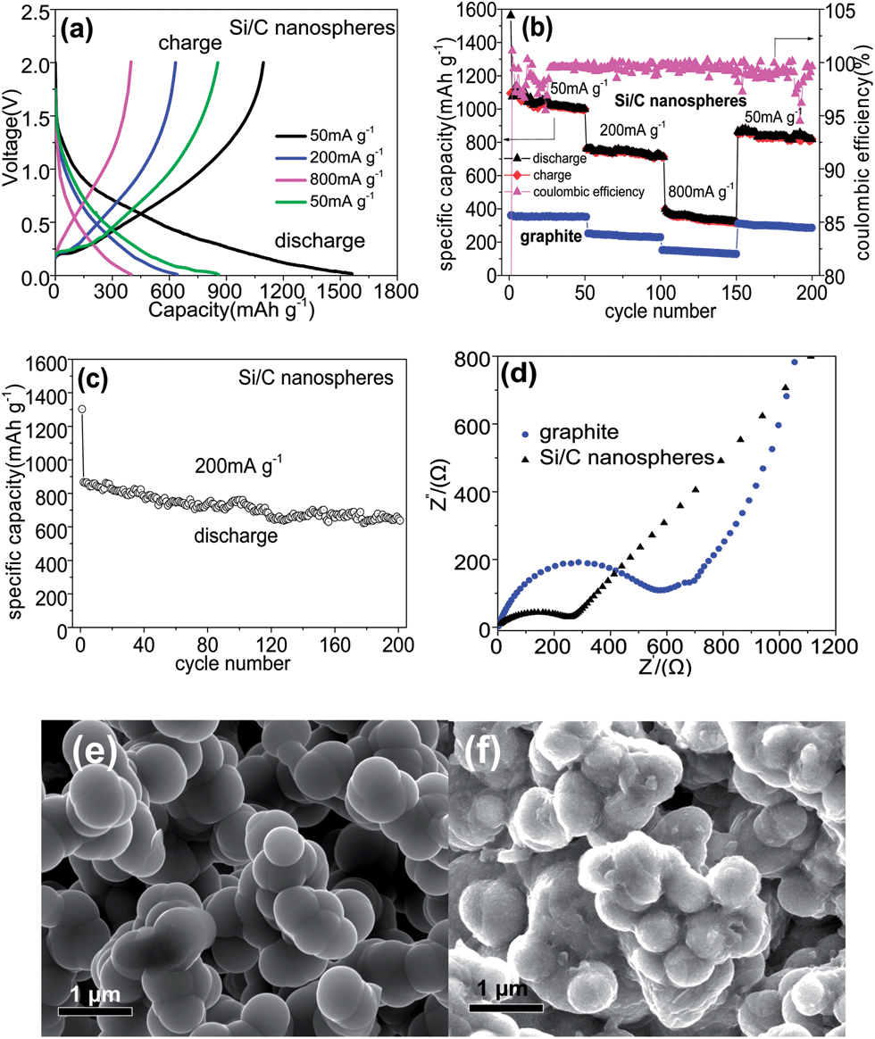 | ||
| Fig. 5 Electrochemical properties of the samples: charge–discharge curves (a) and rate performance (b) at different current densities, cycling property at 200 mA g−1 (c), electrochemical impedance plots (d), and SEM images of Si/C nanospheres before (e) and after 200 charge–discharge cycles (f). | ||
SEM images of linked Si/C nanospheres before (Fig. 5e) and after electrochemical measurement of 200 charge–discharge cycles (Fig. 5f) show that compared with the pristine Si/C nanospheres, the charged Si/C nanospheres still maintain their spherical morphology well. The densification SEI was observed on the surface of Si/C nanospheres, which can explain the excellent discharge capacities of 638.1 mA h g−1 over 200 cycles.80,81 The significant improvement of the lithium storage properties for the binder-free linked Si/C nanospheres is attributed to the following advantages: firstly, the incorporation of the Si and CuxSi nanocrystals within AC can provide high capacity;72,82 secondly, CuxSi, Cu, and AC can absorb the huge volume change of Si during the Li insertion and extraction reactions, thus hindering the cracking or crumbling of the electrode;25,26,69 thirdly, the CuxSi,68 Cu,83 and AC84 improve the electrical conductivity of Si, increasing it from the current collector to each individual Si active particle; and finally, the randomly linked nanostructure of nanospheres directly connected to the Cu substract as binder-free anode can facilitate fast transport of electrons and lithium ions, leading to a remarkably improved reversible capacity and cycling stability.85,86
It should be noted that the linked Si/C nanospheres synthesized in this work still show a relatively low capacity as compared to the theoretical Si capacity, and less stable cycling property than the graphite anode, possibly due to the low content of Si nanocrystals (most are SiOx compounds) and insufficient conductivity of AC. Further work is indeed needed. On the other hand, numerous methylchlorosilanes generated from the organosilane industry could be employed as the precursors. As we know, the CVD method has been widely employed in the preparation of many materials such as carbon nanotubes and Si nanomaterials not only in labs but also in industry. Thus, the large-scale production of linked Si/C nanospheres is possible combining the industrial manufacture of carbon black or white carbon black (SiO2) via CVD process.
4. Conclusions
In summary, we have demonstrated a one-step synthesis of linked Si/C nanospheres grown on Cu substrate by the CCVD approach at 900 °C using CH3SiCl3 precursor. The Si/C nanospheres with a diameter of 400–500 nm are composed of Si, CuxSi, and Cu nanocrystals, which are highly dispersed in the AC matrix. These nanospheres on Cu substrate as an integrated anode material for Li-ion batteries show an excellent lithium storage performance because of the high capacity of Si nanocrystals and good electrical conductivity of CuxSi and Cu nanocrystals embedded within AC, as well as the buffer effect of AC for volume change of Si during the Li insertion and extraction reactions. The network structure of randomly linked nanospheres also can enhance the electron and lithium transport. More importantly, the use of CH3SiCl3, which is less toxic, inflammable, and much cheaper as compared to SiH4 as the Si precursor, is expected to significantly lower the cost of such Si/C composite materials, making feasible the industrial production of Si/C anode materials.Acknowledgements
The authors gratefully acknowledge support from the National Natural Science Foundation of China (no. 51272252), the State Key Laboratory of Multiphase Complex Systems of China (no. MPCS-2012-A-09), and the Hundred Talents Program of the Chinese Academy of Sciences.References
- J. R. Dahn, T. Zheng, Y. H. Liu and J. S. Xue, Science, 1995, 270, 590 CAS.
- K. Sato, M. Noguchi, A. Demachi, N. Oki and M. Endo, Science, 1994, 264, 556 CAS.
- C. K. Chan, H. L. Peng, G. Liu, K. McIlwrath, X. F. Zhang, R. A. Huggins and Y. Cui, Nat. Nanotechnol., 2007, 3, 31 CrossRef PubMed.
- A. Vu, Y. Q. Qian and A. Stein, Adv. Energy Mater., 2012, 2, 1056 CrossRef CAS.
- F. F. Cao, Y. G. Guo and L. J. Wan, Energy Environ. Sci., 2011, 4, 1634 CAS.
- C. L. Zhao, Q. Li, W. Wan, J. M. Li, J. J. Li, H. H. Zhou and D. S. Xu, J. Mater. Chem., 2012, 22, 12193 RSC.
- B. Laik, L. Eude, J. P. Pereira-Ramos, C. S. Cojocaru, D. Pribat and E. Rouviere, Electrochim. Acta, 2008, 53, 5528 CrossRef CAS PubMed.
- M. T. McDowell, I. Ryu, S. W. Lee, C. M. Wang, W. D. Nix and Y. Cui, Adv. Mater., 2012, 24, 6034 CrossRef CAS PubMed.
- Y. Yu, L. Gu, C. B. Zhu, S. Tsukimoto, P. A. van Aken and J. Maier, Adv. Mater., 2010, 22, 2250 Search PubMed.
- H. Ma, F. Y. Cheng, J. Chen, J. Z. Zhao, C. S. Li, Z. L. Tao and J. Liang, Adv. Mater., 2007, 19, 4067 CrossRef CAS.
- M. Gu, Y. Li, X. L. Li, S. Y. Hu, X. W. Zhang, W. Xu, S. Thevuthasan, D. R. Baer, J. G. Zhang, J. Liu and C. M. Wang, ACS Nano, 2012, 6, 8439 CrossRef CAS PubMed.
- V. P. Phan, B. Pecquenard and F. Le Cras, Adv. Funct. Mater., 2012, 22, 2580 CrossRef CAS.
- D. Munao, J. W. M. van Erven, M. Valvo, E. Garcia-Tamayo and E. M. Kelder, J. Power Sources, 2011, 196, 6695 CrossRef CAS PubMed.
- H. Wu, G. Chan, J. W. Choi, I. Ryu, Y. Yao, M. T. McDowell, S. W. Lee, A. Jackson, Y. Yang, L. B. Hu and Y. Cui, Nat. Nanotechnol., 2012, 7, 309 Search PubMed.
- J. Cho, J. Mater. Chem., 2010, 20, 4009 RSC.
- B. M. Bang, J. I. Lee, H. Kim, J. Cho and S. Park, Adv. Energy Mater., 2012, 2, 878 CrossRef CAS.
- A. M. Chockla, K. C. Klavetter, C. B. Mullins and B. A. Korgel, ACS Appl. Mater. Interfaces, 2012, 4, 4658 CAS.
- A. M. Chockla, T. D. Bogart, C. M. Hessel, K. C. Klavetter, C. B. Mullins and B. A. Korgel, J. Phys. Chem. C, 2012, 116, 18079 CAS.
- M. H. Park, M. G. Kim, J. Joo, K. Kim, J. Kim, S. Ahn, Y. Cui and J. Cho, Nano Lett., 2009, 9, 3844 CrossRef CAS PubMed.
- G. B. Cho, S. Y. Choi, J. P. Noh, Y. M. Jeon, K. T. Jung and T. H. Nam, J. Nanosci. Nanotechnol., 2011, 11, 6262 CrossRef CAS PubMed.
- M. Zhou, T. W. Cai, F. Pu, H. Chen, Z. Wang, H. Y. Zhang and S. Y. Guan, ACS Appl. Mater. Interfaces, 2013, 5, 3449 CAS.
- L. G. Xue, G. J. Xu, Y. Li, S. L. Li, K. Fu, Q. Shi and X. W. Zhang, ACS Appl. Mater. Interfaces, 2013, 5, 21 CAS.
- H. X. Chen, Y. Xiao, L. Wang and Y. Yang, J. Power Sources, 2011, 196, 6657 CrossRef CAS PubMed.
- F. F. Cao, J. W. Deng, S. Xin, H. X. Ji, O. G. Schmidt, L. J. Wan and Y. G. Guo, Adv. Mater., 2011, 23, 4415 CrossRef CAS PubMed.
- S. Yoon, S. I. Lee, H. Kim and H. J. Sohn, J. Power Sources, 2006, 161, 1319 CrossRef CAS PubMed.
- L. W. Ji and X. W. Zhang, Energy Environ. Sci., 2010, 3, 124 CAS.
- I. Kovalenko, B. Zdyrko, A. Magasinski, B. Hertzberg, Z. Milicev, R. Burtovyy, I. Luzinov and G. Yushin, Science, 2011, 334, 75 CrossRef CAS PubMed.
- Y. S. Jung, K. T. Lee and S. M. Oh, Electrochim. Acta, 2007, 52, 7061 CrossRef CAS PubMed.
- J. Yu, H. Zhan, Y. Wang, Z. Zhang, H. Chen, H. Li, Z. Zhong and F. Su, J. Power Sources, 2013, 228, 112 CrossRef CAS PubMed.
- X. Zhu, H. Chen, Y. Wang, L. Xia, Q. Tan, H. Li, Z. Zhong, F. Su and X. Zhao, J. Mater. Chem. A, 2013, 1, 4483 CAS.
- H. S. G. W. Guan, X. Wang, S. M. Chen, Y. Bando and D. Golberg, Chem. Commun., 2011, 47, 12098 RSC.
- S. H. Ng, J. Z. Wang, D. Wexler, K. Konstantinov, Z. P. Guo and H. K. Liu, Angew. Chem., Int. Ed., 2006, 45, 6896 CrossRef CAS PubMed.
- Y. S. Hu, R. Demir-Cakan, M. M. Titirici, J. O. Muller, R. Schlogl, M. Antonietti and J. Maier, Angew. Chem., Int. Ed., 2008, 47, 1645 CrossRef CAS PubMed.
- M. Alias, O. Crosnier, I. Sandu, G. Jestin, A. Papadimopoulos, F. Le Cras, D. M. Schleich and T. Brousse, J. Power Sources, 2007, 174, 900 CrossRef CAS PubMed.
- H. Wolf, Z. Pajkic, T. Gerdes and M. Willert-Porada, J. Power Sources, 2009, 190, 157 CrossRef CAS PubMed.
- A. Magasinski, P. Dixon, B. Hertzberg, A. Kvit, J. Ayala and G. Yushin, Nat. Mater., 2010, 9, 461 CrossRef CAS.
- R. Yi, F. Dai, M. Gordin, H. Sohn and D. Wang, Adv. Energy Mater., 2013 DOI:10.1002/aenm.201300496.
- H. Kim, M. Seo, M. H. Park and J. Cho, Angew. Chem., Int. Ed., 2010, 49, 2146 CrossRef CAS PubMed.
- Y. X. Sun, J. Wang, B. T. Zhao, R. Cai, R. Ran and Z. P. Shao, J. Mater. Chem. A, 2013, 1, 4736 CAS.
- R. Tummala, R. K. Guduru and P. S. Mohanty, J. Power Sources, 2012, 199, 270 CrossRef CAS PubMed.
- F. F. Xia, X. L. Hu, Y. M. Sun, W. Luo and Y. H. Huang, Nanoscale, 2012, 4, 4707 RSC.
- Y. M. Sun, X. L. Hu, J. C. Yu, Q. Li, W. Luo, L. X. Yuan, W. X. Zhang and Y. H. Huang, Energy Environ. Sci., 2011, 4, 2870 CAS.
- C. M. Ban, Z. C. Wu, D. T. Gillaspie, L. Chen, Y. F. Yan, J. L. Blackburn and A. C. Dillon, Adv. Mater., 2010, 22, E145 CrossRef CAS PubMed.
- H. X. Zhang, C. Feng, Y. C. Zhai, K. L. Jiang, Q. Q. Li and S. S. Fan, Adv. Mater., 2009, 21, 2299 CrossRef CAS.
- A. Abouimrane, O. C. Compton, K. Amine and S. T. Nguyen, J. Phys. Chem. C, 2010, 114, 12800 CAS.
- X. S. Zhou, A. M. Cao, L. J. Wan and Y. G. Guo, Nano Res., 2012, 5, 845 CrossRef CAS.
- Y. Li, G. J. Xu, L. G. Xue, S. Zhang, Y. F. Yao, Y. Lu, O. Toprakci and X. W. Zhang, J. Electrochem. Soc., 2013, 160, A528 CrossRef CAS PubMed.
- S. Chen, H. Ji, H. Chou, Q. Li, H. Li, J. Suk, R. Piner, L. Liao, W. Cai and R. Ruoff, Adv. Mater., 2013, 25, 2062 CrossRef CAS PubMed.
- Z. Zhang, M. Zhang, Y. Wang, Q. Tan, X. Lv, Z. Zhong, H. Li and F. Su, Nanoscale, 2013, 5, 5384 RSC.
- E. G. Rochow, J. Am. Chem. Soc., 1945, 67, 963 CrossRef CAS.
- R. J. H. Voorhoeve, J. A. Lips and J. C. Vlugter, J. Catal., 1964, 3, 414 CrossRef CAS.
- Z. Zhang, H. Che, Y. Wang, X. She, J. Sun, P. Gunawan, Z. Zhong and F. Su, ACS Appl. Mater. Interfaces, 2012, 4, 1295 CAS.
- Z. Zhang, H. Che, Y. Wang, J. Gao, L. Zhao, X. She, J. Sun, P. Gunawan, Z. Zhong and F. Su, Ind. Eng. Chem. Res., 2012, 51, 1264 CrossRef CAS.
- I. C. Kim, D. Byun, S. Lee and J. K. Lee, Electrochim. Acta, 2006, 52, 1532 CrossRef CAS PubMed.
- T. P. Smirnova, V. V. Kaichev, L. V. Yakovkina, V. I. Kosyakov, S. A. Beloshapkin, F. A. Kuznetsov, M. S. Lebedev and V. A. Gritsenko, Inorg. Mater., 2008, 44, 965 CrossRef CAS.
- M. Yin, C. K. Wu, Y. B. Lou, C. Burda, J. T. Koberstein, Y. M. Zhu and S. O'Brien, J. Am. Chem. Soc., 2005, 127, 9506 CrossRef CAS PubMed.
- J. Hrbek, J. Vac. Sci. Technol., A, 1986, 4, 86 CAS.
- S. J. Schmieg and D. N. Belton, Surf. Sci. Spectra, 1992, 1, 329 CrossRef CAS.
- V. P. Shinde and P. P. Patil, Electrochim. Acta, 2012, 78, 483 CrossRef CAS PubMed.
- S. C. Ray, C. W. Pao, H. M. Tsai, B. Bose, J. W. Chiou, W. F. Pong and D. DasGupta, Carbon, 2006, 44, 1982 CrossRef CAS PubMed.
- S. E. Rodil, A. C. Ferrari, J. Robertson and W. I. Milne, J. Appl. Phys., 2001, 89, 5425 CrossRef CAS.
- D. C. Smith and A. Barbet, J. Raman Spectrosc., 1999, 30, 319 CrossRef CAS.
- R. M. S. dos Reis, R. L. Maltez, E. C. Moreira, Y. P. Dias and H. Boudinov, Appl. Surf. Sci., 2012, 258, 7395 CrossRef CAS PubMed.
- W. F. Banholzer, N. Lewis and W. Ward, J. Catal., 1986, 101, 405 CrossRef CAS.
- I. Kim, G. E. Blomgren and P. N. Kumta, Electrochem. Solid-State Lett., 2003, 6, A157 CrossRef CAS PubMed.
- I. Kim, P. N. Kumta and G. E. Blomgren, Electrochem. Solid-State Lett., 2000, 3, 493 CrossRef CAS PubMed.
- S. Bourderau, T. Brousse and D. M. Schleich, J. Power Sources, 1999, 81, 233 CrossRef.
- D. C. Johnson, J. M. Mosby, S. C. Riha and A. L. Prieto, J. Mater. Chem., 2010, 20, 1993 RSC.
- B. C. Kim, H. Uono, T. Satou, T. Fuse, T. Ishihara, M. Ue and M. Senna, J. Electrochem. Soc., 2005, 152, A523 CrossRef CAS PubMed.
- Y. M. Kang, M. S. Park, J. Y. Lee and H. K. Liu, Carbon, 2007, 45, 1928 CrossRef CAS PubMed.
- Y. He, Y. H. Wang, X. Q. Yu, H. Li and X. J. Huang, J. Electrochem. Soc., 2012, 159, A2076 CrossRef CAS PubMed.
- U. Kasavajjula, C. S. Wang and A. J. Appleby, J. Power Sources, 2007, 163, 1003 CrossRef CAS PubMed.
- I. Hong, B. Scrosati and F. Croce, Solid State Ionics, 2013, 232, 24 CrossRef CAS PubMed.
- A. M. Wilson and J. R. Dahn, J. Electrochem. Soc., 1995, 142, 326 CrossRef CAS PubMed.
- H. C. Tao, L. Z. Fan and X. H. Qu, Electrochim. Acta, 2012, 71, 194 CrossRef CAS PubMed.
- H. J. Jung, M. Park, Y. G. Yoon, G. B. Kim and S. K. Joo, J. Power Sources, 2003, 115, 346 CrossRef CAS.
- R. Yi, F. Dai, M. L. Gordin, S. R. Chen and D. H. Wang, Adv. Energy Mater., 2013, 3, 295 CrossRef CAS.
- Y. Hwa, W. S. Kim, S. H. Hong and H. J. Sohn, Electrochim. Acta, 2012, 71, 201 CrossRef CAS PubMed.
- E. Pollak, G. Salitra, V. Baranchugov and D. Aurbach, J. Phys. Chem. C, 2007, 111, 11437 CAS.
- V. Chakrapani, F. Rusli, M. A. Filler and P. A. Kohl, J. Phys. Chem. C, 2011, 115, 22048 CAS.
- C. C. Nguyen and S. W. Song, Electrochem. Commun., 2010, 12, 1593 CrossRef CAS PubMed.
- T. L. Chan and J. R. Chelikowsky, Nano Lett., 2010, 10, 821 CrossRef CAS PubMed.
- H. Usui, H. Nishinami, T. Iida and H. Sakaguchi, Electrochemistry, 2010, 78, 329 CrossRef CAS PubMed.
- Y. X. Wang, S. L. Chou, J. H. Kim, H. K. Liu and S. X. Dou, Electrochim. Acta, 2013, 93, 213 CrossRef CAS PubMed.
- B. Wang, X. L. Li, B. Luo, Y. Y. Jia and L. J. Zhi, Nanoscale, 2013, 5, 1470 RSC.
- J. Qu, H. Q. Li, J. J. Henry, S. K. Martha, N. J. Dudney, H. B. Xu, M. F. Chi, M. J. Lance, S. M. Mahurin, T. M. Besmann and S. Dai, J. Power Sources, 2012, 198, 312 CrossRef CAS PubMed.
| This journal is © The Royal Society of Chemistry 2014 |