Rational design of carbon network cross-linked Si–SiC hollow nanosphere as anode of lithium-ion batteries†
Zhenhai
Wen
a,
Ganhua
Lu
b,
Shumao
Cui
a,
Haejune
Kim
a,
Suqin
Ci
a,
Junwei
Jiang
c,
Patrick T.
Hurley
c and
Junhong
Chen
*a
aDepartment of Mechanical Engineering, University of Wisconsin-Milwaukee, Milwaukee, Wisconsin 53211, USA. E-mail: jhchen@uwm.edu
bDepartment of Mechanical Engineering, University of Alaska Anchorage, Anchorage, AK 99508, USA
cGlobal Technology & Innovation, Power Solutions, Johnson Controls, Milwaukee, WI 53209, USA
First published on 7th November 2013
Abstract
This study aims to realize controllable synthesis of Si-based nanostructures from common and easily accessible silica nanoparticles and to study their component/structure-dependent electrochemical performance as an anode of lithium-ion batteries (LIBs). To this end, a controllable route based on deliberate design has been developed to prepare hollow Si-based nanospheres with tunable composition and crystal structure at the nanoscale. The synthesis process started with coating silica nanoparticles with a carbonaceous polymer with a controllable thickness followed by magnesiothermic reduction. An Si–SiC–C composite was finally produced with a unique hollow sphere structure featuring Si–SiC nanoparticles encapsulated by a cross-linked carbon film network. In addition to the scalability of the synthetic route, the resulting composite exhibits a number of advantageous properties, including excellent electrical conductivity, highly accessible surfaces, structural coherence, and a favorable structure for the formation of a stable solid-electrolyte interphase, which makes it attractive and promising for advanced anode materials of LIBs.
Introduction
Silicon (Si), due to its attractive physical and chemical properties, has been widely used in various technologies, including nanoelectronics, optoelectronics, bio- and chemical sensors, as well as energy storage and conversion.1–3 Moreover, silicon is nontoxic and naturally the second most abundant element in Earth's crust. It is thus optimistically anticipated that Si will play an increasingly important role and become a stronger driving force in future technologies. A typical example is that Si can be alloyed with lithium and theoretically store energy at a capacity as high as 4200 mA h g−1, being one order of magnitude higher than that of graphite (372 mA h g−1). For this reason, Si has been considered as one of the most competitive alternatives to the current commercial graphite anode materials used in lithium-ion batteries (LIBs). However, there are still at least three critical issues to be addressed in Si-based anodes.4–7 The first and foremost is the huge volume change (>300%) during the alloying–dealloying processes that could induce enormous mechanical stress, structural pulverization, and electrical disconnection from the current collector, leading to a drastic fading in capacity upon cycling. Another disadvantage is their poor electrical conductivity, leading to capacity loss or inefficient utilization of Si. The third challenge is designing and synthesizing Si-based nanostructures that are conducive to form a stable solid-electrolyte interphase (SEI) at the interface between the silicon and the electrolyte so that a long cycle life can be achieved.Therefore, an ideal Si-based anode should be elaborately designed and fabricated to possess a favorable morphology, an excellent conductivity, and a proper porous structure.8–10 Significant efforts have been made to produce various Si nanostructures because nanostructured materials show better capability to withstand stresses from volume changes than the corresponding bulk materials.11–13 Accordingly, a wide variety of Si nanostructures have been designed and fabricated using various synthetic techniques, including chemical vapor deposition (CVD), laser ablation, chemical-assisted thermal disproportionation, electrospin, and template techniques.14–18 Significant progress has been made in improving the electrochemical performance of Si-based anodes through various strategies, including controlling the morphology and structures,19,20 using a buffer matrix such as Si–carbon composites,21–23 and fabricating Si nanoparticles,24 nanowires,25 porous Si materials,26 and core–shell structures.27,28 For example, Yushin et al. developed a bottom-up assembly route for the synthesis of high-performance anodes with Si-decorated carbon black spheres, which can offer irregular channels for rapid access of Li ions and ample internal porosity for accommodating volume changes during cycling.29 Cui's and Cho's groups have conducted extensive research in this field and reported the synthesis of a series of nanostructured Si anodes, including solid, hollow, one-dimensional (1D), and core–shell structures.4,30–35 Through a rational design, these Si nanostructures exhibited a remarkable improvement in electrochemical performance by addressing some existing issues for Si-based anodes. Despite the advancements, it is believed that more research is still required before the final goal of commercial Si-based anodes can be accomplished, specifically, achieving competitive performance, lowering the total cost, and realizing large-scale production.
It was previously reported that the reduction of silica could occur at about 650 °C with magnesium as the reducing agent. Additionally, the structure and the shape of the original silica-based materials can be preserved during this process.36 Therefore, the magnesiothermic reduction process is expected to be amenable for scale-up production of Si nanostructures with precisely controlled microscale shapes and nanoscale features. Meanwhile, it is well known that the Stöber method represents a very classic and mature technology for preparing silica nano- or microspheres.37 Assuming that the above two techniques, i.e., the Stöber recipe and the magnesiothermic method, are combined, it should be promising to develop Si-based nanospheres in large quantities at a low cost. Unfortunately, little work has been done to design, explore, and develop high-performance Si-based anodes from Stöber's SiO2 nanospheres.38,39
In this work, a deliberate design and a controllable route have been developed to realize a controllable synthesis of Si-based hollow nanospheres from common and easily accessible silica nanoparticles. The new Si–SiC–C composite features a hollow, spherical Si–SiC nanohybrid structure encapsulated by a conductive carbon cross-linked network, which endows the composite with a variety of advantageous properties for LIB applications (Fig. 1): (1) the presence of inner voids in the hollow nanospheres offers space for accommodation of Si volume expansion and thus effectively alleviates the mechanical stress; (2) the unique Si–SiC core–shell structure forces the Si volume expansion toward the inner void only given the high mechanical strength of SiC, which ensures the structural integrity of Si-based nanospheres during cycling; (3) the highly porous structure of SiC enables the transport of ions and electrolytes to the Si core, which facilitates the reactions between Si and Li; (4) the presence of a strong SiC layer can be beneficial for forming a stable SEI layer, which improves the cycle performance of the anode; (5) the interconnected carbon network between nanospheres provides an effective channel for electron transfer, which leads to a high electrical conductivity of the anode material.
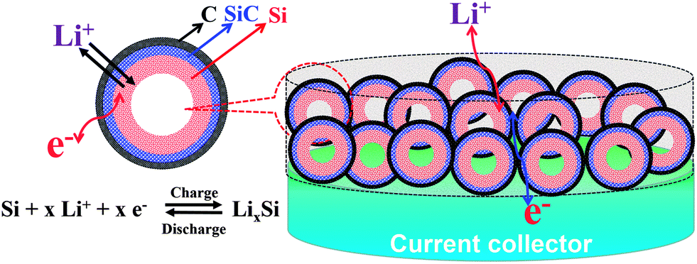 | ||
| Fig. 1 Schematic illustration of the Li+ insertion/deinsertion reaction in the designed Si/SiC@C anode for LIBs. | ||
Results and discussion
Fig. 2 schematically illustrates the entire process for preparing a series of Si-based products. First, a modified Stöber's method was used to prepare a silica nanoparticle colloid, which was then mixed with a glucose solution containing cetyltrimethylammonium bromide (CTAB). A subsequent hydrothermal treatment resulted in composites of carbon-coated SiO2 (SiO2@C). The dried SiO2-based samples were then reduced to Si-based materials through the magnesiothermic reduction reaction, and meanwhile, the as-produced Si reacted with the carbon film covered on its surface (reactions (1) and (2)).| 2Mg + SiO2 →2MgO + Si | (1) |
| Si + C → SiC | (2) |
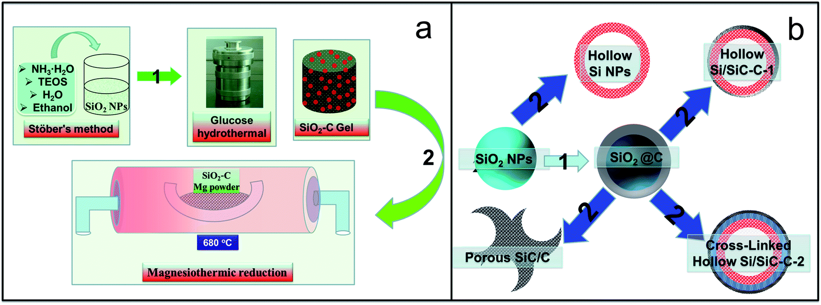 | ||
| Fig. 2 (a) Schematic illustration for the synthesis of hollow Si-based nanosphere composites and (b) a description of the controlled synthesis of various Si-based nanohybrids: (1) modifying SiO2 with a carbonaceous polymer film through hydrothermal treatment of the glucose–SiO2 colloid solution; (2) magnesiothermic reduction of carbon-coated SiO2 nanospheres. | ||
It should be noted that the amount of carbonaceous coating on SiO2 particles can be controlled through adjusting the reaction time or the glucose concentration. In this work, we prepared a series of samples with a hydrothermal reaction time of 2, 4, and 8 hours, respectively, i.e., SiO2@C-1 (Fig. 3c), SiO2@C-2 (Fig. 3e), and SiO2@C-3 (Fig. 3g), which show a color change from grey, brown, to black, demonstrating an increased carbon content with increasing hydrothermal reaction time. After magnesiothermic reduction reaction, the pure SiO2 (Fig. 3a), SiO2@C-1, SiO2@C-2, and SiO2@C-3 samples were converted into a series of Si-based materials denoted as Si (Fig. 3b), Si–SiC/C-1 (Fig. 3d), Si–SiC/C-2 (Fig. 3f), and SiC–C (Fig. 3g), respectively, which also show a distinct color change from light grey, dark grey, to black.
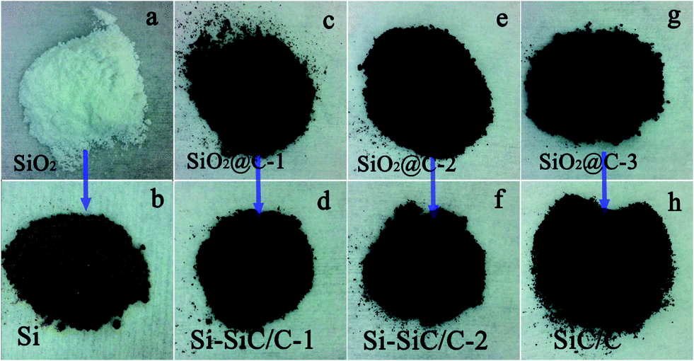 | ||
| Fig. 3 Digital images of the SiO2- and Si-based products, (a) SiO2; (b) Si; (c) SiO2@C-1; (d) Si–SiC/C-1; (e) SiO2@C-2; (f) Si–SiC/C-2; (g) SiO2@C-3; (h) SiC–C. | ||
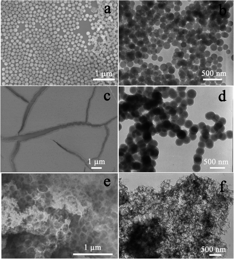
X-ray powder diffraction (XRD) was then carried out on all Si-based samples coupled with scanning electron microscopy (SEM) techniques to investigate the composition, crystalline structure, and morphology of the products. As expected, SiO2 can well evolve into Si (Fig. 4a) after the magnesiothermic reduction treatment, which leads to three peaks that can be indexed to a diamond-structured Si (JCPDS, no. 27-1402). Another three peaks appear after the reduction of SiO2@C samples (Fig. 4b–d), and they correspond with (111), (200), and (220) planes of cubic 3C polytype of silicon carbide (SiC). With an increasing carbon content in SiO2@C, SiC characteristic peaks become more and more apparent accompanied by abatement of the Si peak, indicating that the reaction occurs between Si and carbon with the formation of SiC. Actually, the SiC peaks become dominant for the sample SiO2@C-3 (Fig. 4d), indicating that almost all of the silicon is converted into SiC. Fig. 5 shows the representative SEM images of the Si, Si–SiC/C-1, Si–SiC/C-2, and SiC–C samples, respectively. The first three samples basically maintain the spherical morphology of monodispersed SiO2 nanospheres with a diameter of ∼200 nm. The difference among them is that the Si samples consist of individual nanospheres (Fig. 5a and b), and the nanospheres are connected in Si–SiC/C-1 samples (Fig. 5c and d), while the Si-based nanospheres in Si–SiC/C-2 are embedded in carbon that forms a network structure (Fig. 5e and f). For SiC–C, one can see a three-dimensional (3D) macroporous structure with no observable nanospheres (Fig. 5g and h), which is consistent with the previous report.39
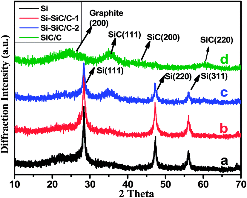 | ||
| Fig. 4 XRD patterns of (a) Si, (b) Si–SiC/C-1, (c) Si–SiC/C-2, and (d) SiC/C. | ||
 | ||
| Fig. 5 SEM images of Si (a and b), Si–SiC/C-1 (c and d), Si–SiC/C-2 (e and f), and SiC/C (g and h). | ||
With SiO2@C-2 as an example, we applied both SEM and transmission electron microscopy (TEM) techniques to investigate the morphology and structure evolution during the synthetic process, as shown in Fig. 6. The as-prepared SiO2 through the Stöber route shows monodispersed nanospheres with a diameter of ∼200 nm (Fig. 6a and b). The hydrothermal treatment with a glucose solution led to the formation of a brown SiO2–C gel (Fig. S1†). According to SEM images, the resulting SiO2–C gel, i.e., SiO2@C-2, exhibits several agglomerated blocks rather than separated SiO2 nanospheres (Fig. 6c). TEM images reveal that SiO2 nanoparticles are actually coated and linked together by a carbonaceous polymer (Fig. 6d). To confirm the structure of the carbonaceous polymer, SiO2 nanospheres were removed by wet etching; the remaining carbonaceous framework does form a 3D carbon network, as displayed in Fig. 6e and f. According to elemental mapping and energy-dispersive X-ray spectroscopy (Fig. S2†), the as-obtained Si–SiC/C-2 shows a uniform distribution of Si and C in the samples and is comprised of 48.5 wt% Si, 16.4 wt% C, and 35.1 wt% O, respectively. Thermogravimetric analysis (TGA, Fig. S3†) shows that there are two main weight loss events over the entire temperature range performed. The first weight loss is about 18% occurring below 250 °C due to the evaporation or desorption of water; and the second weight loss is about 7% in the range of 400–550 °C corresponding with burning of carbon. A slight weight increase is observed at a temperature above 550 °C, which could be attributed to the oxidation of Si.
 | ||
| Fig. 6 SEM and TEM images of (a and b) SiO2, (c and d) SiO2@C-2, (e and f) carbon network after removing SiO2. | ||
The strategy reported here has several advantages for the synthesis of Si-based nanostructures. A major advantage is that the as-developed method offers an effective, low-cost, and controllable route to tailor the components of Si, C, and SiC and also potentially serves as a versatile tool to adjust nanostructures of Si-based materials, which can be readily accomplished by regulating the carbonaceous modification, i.e., the hydrothermal reaction time or the precursor solution. Specifically, more carbon modification can increase the content of carbon and SiC and facilitate the formation of a cross-linked structure, while no or less carbon modification tends to form a separated or weakly connected structure. In this way, functional properties of Si can be adjusted for various applications. Another advantage is the possible large-scale production of such Si-based composites with a wide range of diameters because of easy access of size-tunable SiO2 nano- or macro-spheres using the Stöber method, which enables parametric studies about effects of size, structure, and composition on electrochemical properties of Si-based anodes. The third merit is that carbon can function as a network building block linking hollow Si-based nanospheres as well as a conducting channel for electron transport. Finally, the entire procedure occurs at a relatively moderate temperature (<700 °C), which, along with the fact that no special facility is necessary, is more appealing than conventional methods, such as carbonthermic reduction method.
X-Ray photoelectron spectroscopy (XPS) measurements were carried out to investigate the surface chemical composition of Si–SiC/C-2. Fig. 7a shows the survey spectra of Si–SiC/C-2, in which one can observe several distinct peaks at around 95.5, 151.9, and 285.2 eV, corresponding with Si2p Si2s, C1s spectra, respectively. The distinct peak at 530.3 eV is ascribed to O1s spectra from adsorbed O, tape substrate, Si–O, and carboxyl in samples.30Fig. 7b displays the high resolution XPS spectrum of the Si2p, which shows a strong Si–Si peak at a binding energy of 99.0 eV, a second Si–C peak at 100.9 eV, and a weak Si–O peak at 102.6 eV, respectively.40,41 Further analysis of the spectra can yield surface atomic fractions for each of the constituents. It was estimated that the samples had a molar ratio of Si![[thin space (1/6-em)]](https://www.rsc.org/images/entities/char_2009.gif) :SiC of 2.3:1. The C1s spectrum can also be fitted into three peaks, corresponding with carbide carbon from SiC, graphite carbon, and carboxyl carbon, respectively (Fig. 7c). Raman spectroscopy was further performed to study the chemical composition of the series of samples of Si–SiC/C-1, Si–SiC/C-2, and SiC–C (Fig. S4†). Both Si–SiC–C samples display vibrational peaks at about 500 cm−1 attributable to Si. The Si peak intensity is evidently different in the order of Si–SiC/C-1 > Si–SiC/C-2 > SiC–C, implying that Si increasingly reacts with carbon upon the increase of the carbon content. Additionally, two peaks at ∼1320 and ∼1585 cm−1 can be observed for all samples, which can be assigned to D and G peaks of graphite, respectively. The graphite peaks become obvious especially in the SiC–C nanohybrids due to the excess carbon.
:SiC of 2.3:1. The C1s spectrum can also be fitted into three peaks, corresponding with carbide carbon from SiC, graphite carbon, and carboxyl carbon, respectively (Fig. 7c). Raman spectroscopy was further performed to study the chemical composition of the series of samples of Si–SiC/C-1, Si–SiC/C-2, and SiC–C (Fig. S4†). Both Si–SiC–C samples display vibrational peaks at about 500 cm−1 attributable to Si. The Si peak intensity is evidently different in the order of Si–SiC/C-1 > Si–SiC/C-2 > SiC–C, implying that Si increasingly reacts with carbon upon the increase of the carbon content. Additionally, two peaks at ∼1320 and ∼1585 cm−1 can be observed for all samples, which can be assigned to D and G peaks of graphite, respectively. The graphite peaks become obvious especially in the SiC–C nanohybrids due to the excess carbon.
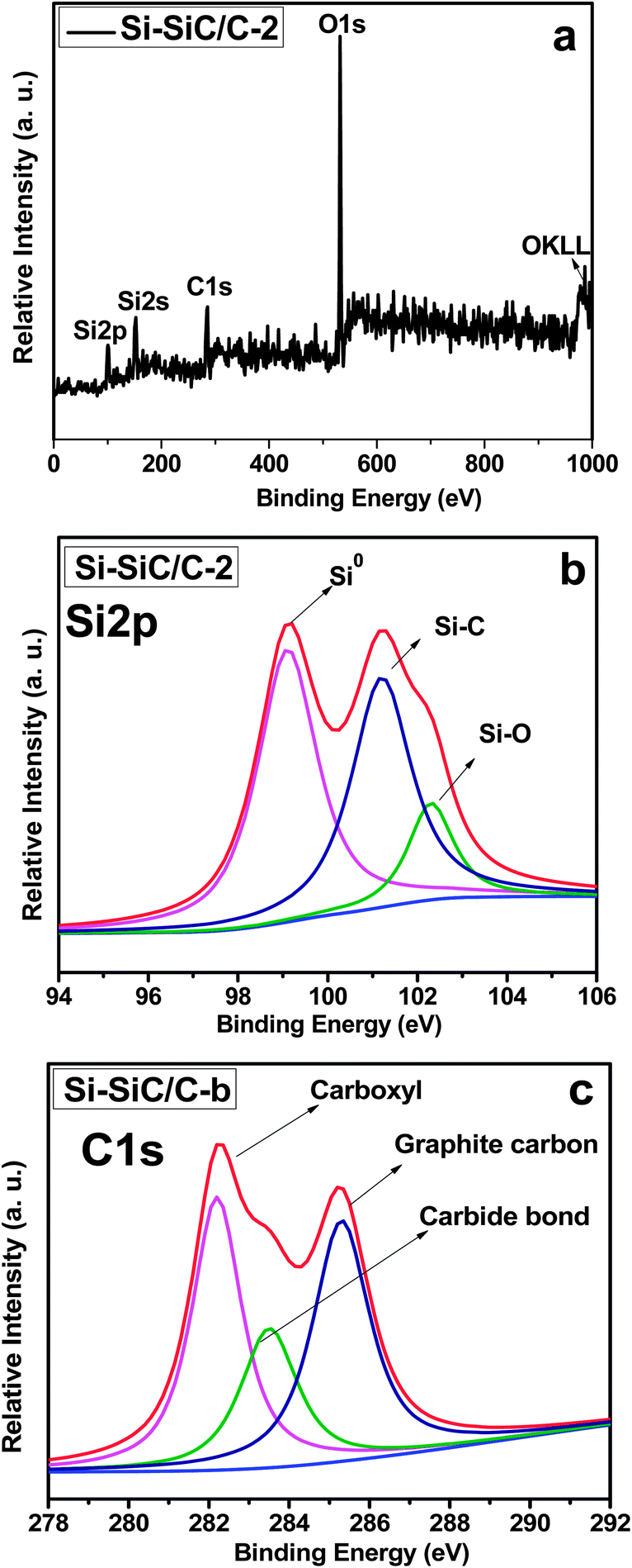 | ||
| Fig. 7 (a) Survey XPS spectrum of Si–SiC/C-2 and high-resolution XPS spectra of (b) Si 2p and (c) C 1s in Si–SiC/C-2. | ||
The properties of porous structure and surface area were investigated through the nitrogen adsorption–desorption measurement in samples of Si, Si–SiC/C-1, Si–SiC/C-2, and SiC–C. All of the four samples exhibit an isotherm curve with a distinct hysteresis loop at the high relative pressure region (Fig. 8a), which is a characteristic of different processes between adsorption into and desorption from mesopores and macropores. According to reports of the nitrogen adsorption–desorption testing, the Si nanosphere displays a BET surface area of 188.0 m2 g−1, which is much lower than those of the other three composites. The Si–SiC/C-1 exhibits a BET surface area of 349.0 m2 g−1, smaller than that of Si–SiC/C-2 (409.1 m2 g−1), suggesting the carbon modification contributes to the improvement of the surface area. The SiC–C presents a slightly lower surface area (398.3 m2 g−1) than that of Si–SiC/C-2, which implies that further reaction between Si and carbon leads to a decrease in the surface area. The corresponding pore-size distribution curves are plotted based on the Barrett–Joyner–Halenda (BJH) method (Fig. 8b); all of the samples exhibit an average pore size around 3.8 nm, while an additional broad peak appears at around 12.2 nm for Si–SiC/C-2 and 9.8 nm for SiC–C samples, respectively, which could be assigned to the pores at the interface of C–Si produced by the reaction between carbon and Si.
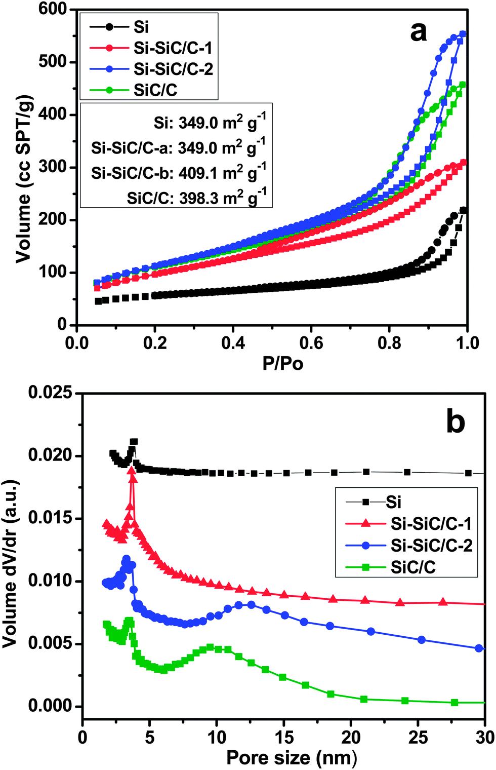 | ||
| Fig. 8 Nitrogen adsorption–desorption isotherms obtained at 77 K (a) and pore size distribution (b) of Si (black), Si–SiC/C-1 (red), Si–SiC/C-2 (blue), and SiC/C (green). | ||
The electrochemical lithium storage properties of various Si-based materials were further examined by using a galvanostatic charge–discharge method at a current density of 500 mA g−1. Fig. 9 shows the discharge and charge profiles during the initial two cycles in a coin-type half-cell between 0.01 and 2.0 V at a current density of 500 mA g−1. The first discharge profile displays a long and flat plateau below 0.1 V due to the reaction of crystalline Si with Li with the formation of LixSi. And the charge profile exhibits a plateau at ∼0.45 V corresponding with delithiation of LixSi to Si. The charge–discharge profiles are basically consistent with previous reports.26,34 Specifically, the Si displays initial discharge and charge capacities of 2564 and 999 mA h g−1, respectively, corresponding with a Coulombic efficiency (CE) of 39.0%. The Si–SiC/C-1 shows a slightly higher CE of 41% with increased discharge and charge capacities of 2910 and 1120 mA h g−1. As expected, the Si–SiC/C-2 delivered a relatively lower discharge capacity of 2340 mA h g−1 due to the presence of SiC that is normally viewed as an inactive matrix42 and carbon that has a lower specific capacity. However, there was a significant improvement of CE for Si–SiC/C-2 in the first cycle, which delivered a charge capacity of 1705 mA h g−1 and attained a CE of around 72.9%. The initial CE value for Si–SiC/C-2 is much higher than those of other electrodes, which is likely due to the appropriate composition of Si–SiC-2 (i.e., C, Si, and SiC) and a unique core–shell hollow nanosphere structure, i.e., the interconnected carbon network that is conducive for improved electrical conductivity, the intermediate layer of SiC that favors the formation of a stable SEI, and the void in the hollow structure that offers space to alleviate the volume change issue of Si anodes during charging–discharging cycles. After the initial cycle, the Coulombic efficiency gradually reached a relatively steady-state value in the following cycles for all electrodes (Fig. S5†). Because SiC became dominant in the case of SiC–C, the initial discharge and charge capacity drastically decreased to 753 and 285 mA h g−1, respectively, likely due to the irreversible electrochemical reaction of SiC materials.43 The electrochemical properties of the Si–SiC/C-1 and Si–SiC/C-2 samples as anode of LIB were further evaluated using cyclic voltammetry (CV). There is a pronounced decrease in the cathodic current between the first and the second cycle for the Si–SiC/C-1 due to the irreversible reactions and the formation of an SEI layer while the Si–SiC/C-2 sample displays a smaller change in the initial two CV curves than the Si–SiC/C-1 sample (Fig. S6†), confirming less capacity loss in the initial two cycles for Si–SiC/C-2.
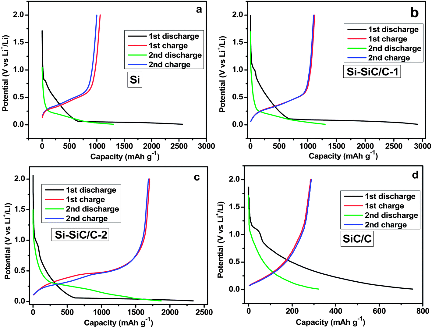 | ||
| Fig. 9 Initial two charge–discharge profiles for Si (a), Si–SiC/C-1 (b), Si–SiC/C-2 (c), and SiC/C (d). | ||
Electrochemical impedance spectroscopy (EIS) measurements were conducted to study the resistance associated with the series of Si-based materials. Fig. 10a shows the Nyquist plots recorded for the Si, Si–SiC/C-1, Si–SiC/C-2, and SiC–C half-cells, respectively, all of which consist of a depressed semicircle in the moderate frequency region corresponding with the charge transfer resistances (Rct). It was revealed that the Rct for the Si–SiC/C-1 (13.8 Ω) and Si–SiC/C-2 (16.7 Ω) was an order of magnitude lower than that of a pure hollow Si nanosphere (177.9 Ω), suggesting that the carbon modification does significantly improve the electrical conductivity of the Si-based anode. Fig. 10b profiles the cycling performance of three samples at a current density of 500 mA g−1. Generally, all of the three electrodes show a decrease of capacity during cycling, which could be attributed to irreversibility resulting from the formation of SEI, the electrode pulverization, irreversible alloy–de-alloy reaction, and the defect structure on the carbon.7,10 After 80 charge–discharge cycles, the Si–SiC/C-2 maintained a capacity of about 937 mA h g−1, a significantly higher value than the theoretical specific capacity of the commercialized graphite anode material, and also much higher than the corresponding capacity of Si (501 mA h g−1) and Si–SiC/C-1 (690 mA h g−1). We further investigated the impedance change for Si–SiC/C-1 and Si–SiC/C-2 samples upon cycling. Because the SiC is a semiconductor instead of a conductor, it is reasonable that the Si–SiC/C-1 showed a slightly lower Rct than the Si–SiC/C-2, since the former contains a smaller fraction of SiC. However, the Si–SiC/C-1 exhibits an evident impedance change upon cycling with the Rct varying from 13.8 to 28.2 Ω over 80 cycles (Fig. 10c). In contrast, the Si–SiC/C-2 only shows a slight change only in impedance spectroscopy, corresponding with an Rct change from 16.7 to 18.3 Ω after 80 cycles (Fig. 10d). These results confirm that the Si–SiC/C-2 can well maintain the high conductivity upon cycling, possibly due to the stable structure enabled by the buffer matrix of SiC, which in turn improves its electrochemical performance.35 It should be noted that both SiC–C and carbon delivered an initial capacity of below 800 mA h g−1 (Fig. S7†), which is much lower than those of Si–SiC–C composites, implying that the capacity of the Si–SiC/C-2 sample is mainly attributed to silicon. On the other hand, SiC–C and carbon almost achieved a stable capacity in the second cycle, confirming that carbon and SiC can be beneficial for the formation of a stable SEI.
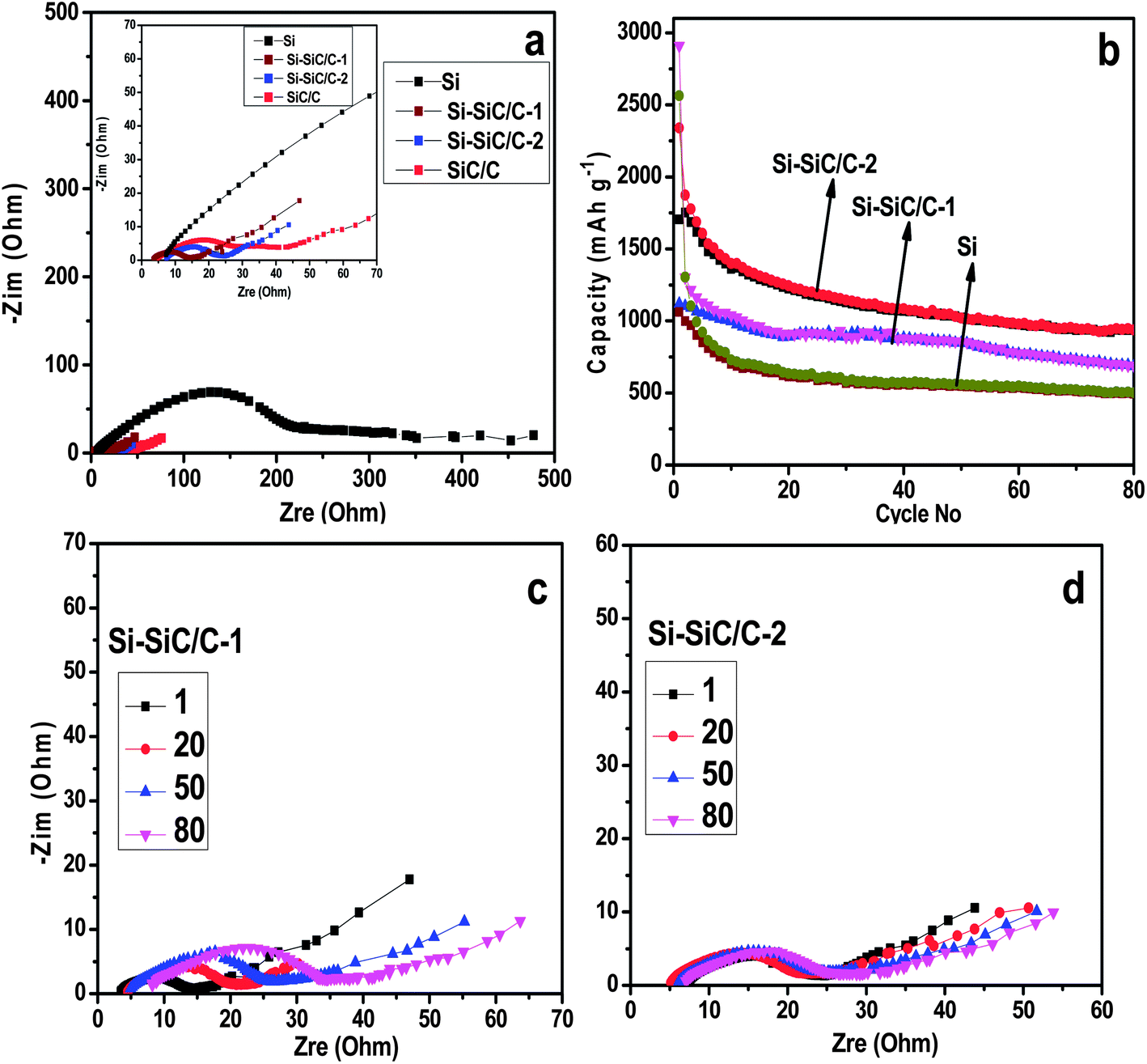 | ||
| Fig. 10 Nyquist curve (a) and cycle performance (b) of LIBs with Si, Si–SiC/C-1, and Si–SiC/C-2 as working electrodes, the inset of (a) is the corresponding magnified curve in the high frequency region. Evolution of Nyquist curves of LIBs with Si–SiC/C-1 (c) and Si–SiC/C-2 (d) during cycling. | ||
The detailed structure of the Si–SiC/C-2 was further studied by TEM to explore its intrinsic nanostructure and to better understand the improved electrochemical performance. Fig. 11a shows a typical TEM image with a low magnification, which clearly illustrates that the sample has uniform interconnected hollow spheres with a diameter of ∼200 nm. One can also observe a large number of mesopores on the surfaces of spheres. Fig. 11b displays the corresponding selected area electron diffraction (SAED) pattern. The obvious polycrystalline rings can be ascribed to diffraction planes of the diamond-structured Si crystals, and the dotted rings are attributed to diffraction planes of SiC crystals. These results further confirm that the composites are composed of well crystalized Si and SiC. Fig. 11c manifests the edge of one hollow Si–SiC/C-2 composite; the darker fringe reconfirms that the sphere has a hollow structure and suggests that the exterior boundary actually consists of integrated composites. It is reasonable to hypothesize that the galvanic replacement between Mg and SiO2 results in the formation of Kirkendall voids,44,45 because the diffusion of SiO2 and Mg atoms in opposite directions took place on the surfaces of carbon and SiO2, which is consistent with the previous reports.38,39 Meanwhile, the void continues to be emptied as the product Si continues to react with carbon, thereby leading to sandwiched SiC layers between Si and carbon. Further analysis through high-resolution TEM images (Fig. 11d–f) shows that there are three typical types of nanostructures. Type I is a carbon film with a poor crystalline structure, which most commonly appears in the outermost layer of spheres; Type II is a nanocrystal with a lattice spacing of 0.25 nm belonging to the (111) plane of SiC, which is usually dispersed inside the carbon film; Type III is Si nanoparticle, which exhibits a lattice spacing of 0.31 nm corresponding with the (111) plane of Si, which can be easily found especially in the interior surface of hollow structures. It should be noted that, besides the macroporous void provided by removing SiO2 nanospheres, one can also observe mesopores with a size of ∼3 nm, as shown in the outer surface of the hollow sphere, which can facilitate the transport of ions and electrolytes (Fig. 11e). Fig. 11f exhibits a magnified TEM image of the inner surface of the hollow sphere; one can clearly observe the interface (red dotted line) between Si and SiC nanocrystals, confirming that SiC forms at the interface between C and Si.
 | ||
| Fig. 11 (a) TEM image, (b) SAED patterns, and (c–f) HRTEM images of the Si–SiC/C-2. | ||
According to the electrochemical testing results and the detailed analysis above, it is evident that Si–SiC/C-2 showed the best performance as an anode of LIB among all of the Si-based nanocomposites prepared in this study, which is likely attributed to the unique nanostructure in the hybrids. First, Si-based nanoparticles are inside the hollow structures, providing enough room to accommodate large volume changes of Si nanoparticles. In addition, the hollow Si-based nanostructures were embedded in the cross-linked carbon network so that the electrical conductivity of Si–SiC/C-2 can be greatly enhanced and the Ohmic loss could be greatly reduced. Furthermore, the presence of SiC between Si and carbon can effectively buffer the stress produced by the Si expansion during the lithiation process and thus leads to the formation of a stable SEI film on the outer surface. Finally, the formation of a large number of pores (e.g., on the SiC surface and between nanospheres) can facilitate the mass transfer (e.g., ion, electrolyte). It should be noted that the current capacity performance of Si–SiC/C-2 is not the best compared with what has been reported previously.29,35 However, the Si–SiC/C-2 sample exhibits a good rate performance (Fig. S7d†), with a capacity around 350 mA h g−1 even at a current density of 2000 mA g−1. In addition, the Si–SiC/C-2 sample after 80 charge–discharge cycles was investigated by SEM (Fig. S8†); the microsphere structure in the Si–SiC/C-2 sample can be well maintained even after 80 cycles, reconfirming excellent stability of such a structure. Moreover, the electrochemical performance can be further improved based on the fact that the as-developed strategy can control the size, structure, and composition with flexibility and selectivity.
Conclusion
In summary, this work demonstrated an effective and reliable synthetic method to produce hollow nanohybrids of Si–SiC–C composites in a controllable manner. Through a deliberate design, a nanocomposite with hollow Si–SiC nanospheres embedded in a cross-linked porous carbon network, i.e., Si–SiC/C-2, can be prepared. The resulting interconnected hollow Si-based nanospheres exhibit improved electrochemical performance compared with their counterpart Si-based nanohybrids as anodes of LIBs. While the formation of a carbon network leads to a remarkable decrease in the electrical resistance of electrode materials, the presence of SiC between C and Si can contribute to the formation of a stable solid-electrolyte interphase. The present work is expected to open up new opportunities for applications of Si- or SiC- based materials in the fields of sensors, solar cells, and water splitting, with improved performance.Experimental
Materials and synthesis
All of the chemicals were purchased from Sigma-Aldrich without further treatment. Silica nanoparticles were synthesized using Stöber's method with a volume ratio of TEOS:ammonia:water:ethanol = 1:1:2:20 with continuous stirring for 8 hours. The silica colloid solution was then mixed with the same volume of a glucose aqueous solution (1.0 M) containing 2.0 g L−1 CTAB, which was then transferred to a Teflon-lined stainless steel autoclave and heated at 170 °C for 2, 4, 8 hours respectively, to tune the thickness of the carbon film on the silica nanoparticles. The samples after filtering and drying were denoted as SiO2@C-1, SiO2@C-2, and SiO2@C-3, respectively. Afterwards, the silica or SiO2@C samples were sufficiently mixed with Mg powder in a molar ratio of 1:2, and then heated at 680 °C under argon gas protection for 3 hours. The resulting products were then carefully dispersed in a 0.5 M HCl solution under stirring for 1 hour to remove impurities. The silicon-based active materials were obtained by water washing for five times and vacuum drying.
Characterization
The morphology and nanostructures of the samples were investigated using a high-resolution transmission electron microscope (HRTEM) (Hitachi H-9000-NAR) with 0.18 nm point and 0.11 nm lattice resolution operated at an accelerating voltage of 300 kV, and a field-emission scanning electron microscope (SEM) (Hitachi S4800), which is equipped with a Bruker Quantax Energy-dispersive X-ray Spectrometry (EDS) system. The X-ray powder diffraction (XRD) patterns were measured with monochromatized CuKα radiation (λ = 1.5418 Å) on a Scintag XDS 2000 X-ray powder diffractometer between scattering angles (2θ) of 10° and 70°. Raman spectra were obtained on a Raman spectrometer (Renishaw 1000B). X-ray photoelectron spectroscopy (XPS) was conducted using HP 5950A XPS with Mg Kα as source and the C1s peak at 284.6 eV as an internal standard. Specific surface areas were measured through Brunauer–Emmett–Teller (BET) nitrogen adsorption–desorption on a Micromeritics ASAP 2010 instrument (Shimadzu). Thermogravimetric analysis (TGA, Mettler Toledo TGA-SDTA851 analyzer) was conducted from room temperature to 600 °C under air atmosphere with a heating rate of 5 °C min−1.Electrochemical measurements
The working electrode was prepared by first fully mixing active materials (90%), acetylene black (5%), and the carboxymethylcellulose binder (CMC, 5%). The formed pasty was then spread onto a copper foil through a doctor-blade technique, followed by drying in vacuum at 120 °C for 10 h. The coin cell was assembled in an Ar-filled glove box using a lithium pellet as both the counter and the reference electrodes. The electrolyte solution was 1 M LiPF6 dissolved in a mixture of ethylene carbonate (EC), dimethyl carbonate (DMC) with a volume ratio of EC:DMC = 1:1. Cyclic voltammetry was conducted using a CHI 760 electrochemical station with a voltage range of 0–2.0 V at a scan rate of 0.1 mV s−1. Galvanostatic cycling experiments were carried out to study the electrode activities and cycle performance using a Land battery tester system at room temperature. Discharge–charge curves were recorded at a voltage range between 2.0 and 0.01 V. The capacity was calculated based on the total weight of the electrode materials. Electrochemical impedance spectroscopy (EIS) measurements were performed using a CHI760 electrochemical workstation.
Acknowledgements
This work was financially supported by the U.S. Department of Energy (DE-EE0003208) and Johnson Controls. The authors thank Professor M. Gajdardziska-Josifovska for TEM access at the UWM HRTEM Laboratory, Dr H. A. Owen for technical support with SEM analyses, Dr S. E. Hardcastle for technical support with XRD and XPS analyses and Dr M. Piechowski for proofreading the manuscript.References
- R. Soref, Silicon, 2010, 2, 1 CrossRef CAS.
- V. Schmidt, J. V. Wittemann, S. Senz and U. Goesele, Adv. Mater., 2009, 21, 2681 CrossRef CAS.
- J. J. Pla, K. Y. Tan, J. P. Dehollain, W. H. Lim, J. J. L. Morton, D. N. Jamieson, A. S. Dzurak and A. Morello, Nature, 2012, 489, 541 CrossRef CAS PubMed.
- N.-S. Choi, Y. Yao, Y. Cui and J. Cho, J. Mater. Chem., 2011, 21, 9825 RSC.
- A. Esmanski and G. A. Ozin, Adv. Funct. Mater., 2009, 19, 1999 CrossRef CAS.
- J. R. Szczech and S. Jin, Energy Environ. Sci., 2011, 4, 56 CAS.
- C.-M. Park, J.-H. Kim, H. Kim and H.-J. Sohn, Chem. Soc. Rev., 2010, 39, 3115 RSC.
- D. Chen, X. Mei, G. Ji, M. Lu, J. Xie, J. Lu and J. Y. Lee, Angew. Chem., Int. Ed., 2012, 51, 2409 CrossRef CAS PubMed.
- X. Zhou, Y.-X. Yin, L.-J. Wan and Y. G. Guo, Chem. Commun., 2012, 48, 2198 RSC.
- X. L. Wu, Y. G. Guo and L. J. Wan, Chem.–Asian J., 2013, 8, 1948 CrossRef CAS PubMed.
- D. Munao, M. Valvo, J. van Erven, E. M. Kelder, J. Hassoun and S. Panero, J. Mater. Chem., 2012, 22, 1556 RSC.
- J. Y. Choi, D. J. Lee, Y. M. Lee, Y. G. Lee, K. M. Kim, J. K. Park and K. Y. Cho, Adv. Funct. Mater., 2013, 23, 2108 CrossRef CAS.
- N. Hung Tran, M. R. Zamfir, D. Loc Dinh, Y. H. Lee, P. Bondavalli and D. Pribat, J. Mater. Chem., 2012, 22, 24618 RSC.
- H. Zhang and P. V. Braun, Nano Lett., 2012, 12, 2778 CrossRef CAS PubMed.
- J.-K. Yoo, J. Kim, Y. S. Jung and K. Kang, Adv. Mater., 2012, 24, 5452 CrossRef CAS PubMed.
- J. L. Goldman, B. R. Long, A. A. Gewirth and R. G. Nuzzo, Adv. Funct. Mater., 2011, 21, 2412 CrossRef CAS.
- J.-I. Lee, K. T. Lee, J. Cho, J. Kim, N.-S. Choi and S. Park, Angew. Chem., Int. Ed., 2012, 51, 2767 CrossRef CAS PubMed.
- T. H. Hwang, Y. M. Lee, B.-S. Kong, J.-S. Seo and J. W. Choi, Nano Lett., 2012, 12, 802 CrossRef CAS PubMed.
- J. W. Wang, X. H. Liu, K. Zhao, A. Palmer, E. Patten, D. Burton, S. X. Mao, Z. Suo and J. Y. Huang, ACS Nano, 2012, 6, 9158 CrossRef CAS PubMed.
- A. Gohier, B. Laik, K.-H. Kim, J.-L. Maurice, J.-P. Pereira-Ramos, C. S. Cojocaru and V. Pierre Tran, Adv. Mater., 2012, 24, 2592 CrossRef CAS PubMed.
- Y. He, X. Yu, Y. Wang, H. Li and X. Huang, Adv. Mater., 2011, 23, 4938 CrossRef CAS PubMed.
- C. Martin, O. Crosnier, R. Retoux, D. Bélanger, D. M. Schleich and T. Brousse, Adv. Funct. Mater., 2011, 21, 3524 CrossRef CAS.
- W. J. Lee, M.-H. Park, Y. Wang, J. Y. Lee and J. Cho, Chem. Commun., 2010, 46, 622 RSC.
- H. Kim, M. Seo, M.-H. Park and J. Cho, Angew. Chem., Int. Ed., 2010, 49, 2146 CrossRef CAS PubMed.
- C. K. Chan, H. Peng, G. Liu, K. McIlwrath, X. F. Zhang, R. A. Huggins and Y. Cui, Nat. Nanotechnol., 2008, 3, 31 CrossRef CAS PubMed.
- H. Jia, P. Gao, J. Yang, J. Wang, Y. Nuli and Z. Yang, Adv. Energy Mater., 2011, 1, 1036 CrossRef CAS.
- L.-F. Cui, Y. Yang, C.-M. Hsu and Y. Cui, Nano Lett., 2009, 9, 3370 CrossRef CAS PubMed.
- H. Kim and J. Cho, Nano Lett., 2008, 8, 3688 CrossRef CAS PubMed.
- A. Magasinski, P. Dixon, B. Hertzberg, A. Kvit, J. Ayala and G. Yushin, Nat. Mater., 2010, 9, 353 CrossRef CAS PubMed.
- N. Liu, H. Wu, M. T. McDowell, Y. Yao, C. Wang and Y. Cui, Nano Lett., 2012, 12, 3315 CrossRef CAS PubMed.
- M.-H. Park, M. G. Kim, J. Joo, K. Kim, J. Kim, S. Ahn, Y. Cui and J. Cho, Nano Lett., 2009, 9, 3844 CrossRef CAS PubMed.
- B. M. Bang, J.-I. Lee, H. Kim, J. Cho and S. Park, Adv. Energy Mater., 2012, 2, 878 CrossRef CAS.
- B. M. Bang, H. Kim, J.-P. Lee, J. Cho and S. Park, Energy Environ. Sci., 2011, 4, 3395 CAS.
- B. M. Bang, H. Kim, H.-K. Song, J. Cho and S. Park, Energy Environ. Sci., 2011, 4, 5013 CAS.
- H. Wu, G. Chan, J. W. Choi, I. Ryu, Y. Yao, M. T. McDowell, S. W. Lee, A. Jackson, Y. Yang, L. Hu and Y. Cui, Nat. Nanotechnol., 2012, 7, 309 Search PubMed.
- Z. Bao, M. R. Weatherspoon, S. Shian, Y. Cai, P. D. Graham, S. M. Allan, G. Ahmad, M. B. Dickerson, B. C. Church, Z. Kang, H. W. Abernathy III, C. J. Summers, M. Liu and K. H. Sandhage, Nature, 2007, 446, 172 CrossRef CAS PubMed.
- A. F. Werner Stöber, J. Colloid Interface Sci., 1968, 26, 62 CrossRef.
- M.-P. Liu, C.-H. Li, H.-B. Du and X.-Z. You, Chem. Commun., 2012, 48, 4950 RSC.
- Y. Shi, F. Zhang, Y.-S. Hu, X. Sun, Y. Zhang, H. I. Lee, L. Chen and G. D. Stucky, J. Am. Chem. Soc., 2010, 132, 5552 CrossRef CAS PubMed.
- P. Mélinon, B. Masenelli, F. Tournus and A. Perez, Nat. Mater., 2007, 6, 479 CrossRef PubMed.
- J. Binner and Y. Zhang, J. Mater. Sci. Lett., 2001, 20, 123 CrossRef CAS.
- I. S. Kim, G. E. Blomgren and P. N. Kumta, J. Power Sources, 2004, 130, 275 CrossRef CAS PubMed.
- A. L. Lipson, S. Chattopadhyay, H. J. Karmel, T. T. Fister, J. D. Emery, V. P. Dravid, M. M. Thackeray, P. A. Fenter, M. J. Bedzyk and M. C. Hersam, J. Phys. Chem. C, 2012, 116, 20949 CAS.
- H. J. Fan, U. Gösele and M. Zacharias, Small, 2007, 3, 1660 CrossRef CAS PubMed.
- W. Wang, M. Dahl and Y. Yin, Chem. Mater., 2013, 25, 1179 CrossRef CAS.
Footnote |
| † Electronic supplementary information (ESI) available. See DOI: 10.1039/c3nr04162j |
| This journal is © The Royal Society of Chemistry 2014 |