DOI:
10.1039/C3NR03911K
(Paper)
Nanoscale, 2014,
6, 405-411
Dynamic investigation of interface atom migration during heterostructure nanojoining†
Received
28th July 2013
, Accepted 2nd October 2013
First published on 7th October 2013
Abstract
Interface atom migration and compositional evolution during the heterostructure nanojoining process under external electrical loadings has been investigated in situ inside a transmission electron microscope with atomic resolution. The results indicate that the migration of oxygen atoms on the contact interface of metal nanorods is a thermal dominated process rather than an electromigration process. After removing the oxide layer at the nanometal contact interface, the metal atoms migrate under external electrical field. The formation region of nanoalloys can be modulated by controlling the electromigration direction of nanometal atoms, leading to an electromigration-dominated cutting process which offers an extra degree of freedom to design a sacrifice layer and interconnects in solid-state bonding. These findings offer an insight of potential failure mechanisms as well as fabrication methodology for interconnects in nanodevices.
Introduction
As the continuous down-scaling of advanced electronic nanodevices, high resolution lithography requires a more precise way to control the chemical composition and structure of nanomaterials.1,2 However, high-resolution nanofabrication and structural optimization of nanomaterials remain challenging due to size effect. For instance, the melting point of a metal decreases dramatically as its grain size decreases;3,4 the reaction activities of nanomaterials increase and their migration barriers are weakened with the increase of their specific area, hereby threatening the reliability of interconnects and device structures;5 the Hall–Petch relation is no longer valid for the nanomaterials with a diameter smaller than the critical size.6–9 Furthermore, dislocation-dominated plasticity for bulk materials changes to grain boundary-dominated plasticity for nanomaterials;7,8 grain size, grain orientation and compositional evolution at the interface between nanoscale metals have a significant influence on the bonding process.10 The transmission electron microscope (TEM)-scanning tunneling microscopic (STM) system enables an in situ observation of the structural evolutions of nanomaterials under diverse loadings, e.g. external stress and electrical pulse. Several recent studies have demonstrated the feasibility of this methodology.11,12,14 Lu et al. reported that the hardness of metallic nanobeams increases remarkably as the nanobeam diameter decreases.12 Kiener et al. revealed that size-dependent yield strength is caused by the dislocation source limitation on Cu structures with diameters less than 400 nm.13 Yu and Misra showed that cold welding and electron beam induced bonding can be achieved easily at the nanoscale.14,15 Tohmyoh et al. carried out a series of experiments which focused on the welding of metal nanowires enabled by Joule heating. They demonstrated a parameter-governed joining phenomenon of Pt wires and the possibility of atom diffusion facilitated by electromigration during Ag nanojoining.16,17 However, the mechanism of compositional and structural evolution of the nanometals and atom migration process at the contact interface under electrical loadings were seldom studied.
In this work, we used electrochemical etched Al and Cu nanorods to implement heterostructure nanojoining. The direction of atom electromigration and the formation of nanoalloys at the interface were observed dynamically under external electrical loadings at the nanoscale. The chemical evolution of the nanometals was studied by energy filtered TEM (EFTEM) imaging techniques.18,19 The results demonstrate a thermal dominated migration process of oxygen atoms at the contact interface of metal nanorods. The formation region of nanoalloys is dependent on the electromigration direction of nanometal atoms, leading to an electromigration-dominated cutting process.
Experimental
In this work, Al nanorods were electrochemically etched in 1.5 mol L−1 HCl solution mixed with 0.25 mol L−1 Na2SO4. The etching voltage was 0.5 V with a compliance current of 10 mA. For Cu nanorods, the etching solution was 2.23 mol L−1 HNO3 and the etching voltage was 4 V with a compliant current of 10 mA. All nanorods were cleaned by plasma cleaning for 30 s to reduce impurities at the surface for in situ TEM experiments.18 High-resolution TEM characterization and electron-energy-loss-spectroscopy measurements were carried out using a Cs-corrected TEM (FEI Titan 80-300) equipped with a TEM-STM platform (Nanofactory AB).
Fig. 1(a) illustrates the configuration of the in situ TEM-STM system. The Al nanorod was fixed onto a movable piezotube as one electrode and the Cu nanorod was fixed on the opposite end as the other electrode. The movement of the Al nanorod was controlled precisely with a step of 20 pm in the X, Y direction and 2.5 pm in the Z direction. Fig. 1(b) shows the schematic view of the in situ TEM characterization setup. The prepared Al and Cu nanorods were covered with a thin metal oxide layer due to the exposure to the air.
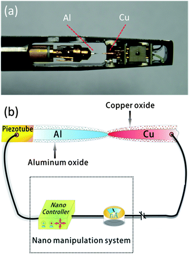 |
| | Fig. 1 (a) Image of an in situ TEM-STM holder. The Al nanorod was controlled by a movable piezotube. (b) Schematic view of the in situ TEM characterization setup. | |
Result and discussion
1. Nanojoining process and oxygen atom migration
The contacts of the two nanorods were implemented by precisely controlling the piezotube. Through selected area electron diffraction (SAED), we found the contact region was made up of polycrystals (see ESI Fig. 5*†). A constant bias was applied onto the two nanorods. Both nanorods were initially covered with a thin metal oxide layer, thus the ohmic contact could not be achieved unless the oxygen atoms migrated away from the interface. The applied constant bias gradually generated Joule heating at the contact region, thus facilitating the migration of oxygen atoms. Electromigration and thermal diffusion might be involved in the oxygen atom migration process. To figure out the main mechanism of oxygen atom migration, EFTEM analysis was applied during the process. Fig. 2(a)–(c) show a sequence of oxygen maps. The energy width was set to be 10 eV with a center at 532 eV for oxygen. The exposure time range of all the mappings was fixed at 10 s. The Cu side was subjected to a negative voltage of 2 V during the entire bonding process. Initially, the current density at the interface was less than 106 A m−2, which is far below the threshold current density (109 to 1011 A m−2) of electromigration.20,21 The ohmic contact was completed within 37 min (the current density was about 5 × 10⁷ A m−2 at that point). By comparing the mean signal density of oxygen at the top sampling region and the body sampling region at different times, we observed that the oxygen signal ratio of the two nanorods decreased significantly under electrical loading (Fig. 2(d)). If the electromigration effect dominated the migration process, the oxygen signal ratio of the two nanorods should demonstrate an opposite tendency because of unidirectional migration (which contradicts Fig. 2(d)). Given that the current flowing through the oxide layer with high resistance is minimal even after the completion of ohmic contact, this layer should not be significantly influenced by electromigration. Therefore, oxygen atom migration is a thermal-dominated process. The heat generated at the interface was from applied constant bias and electron beam irradiation (although the increase of temperature caused by electron beam irradiation was comparatively minimal, see ESI†). The oxide signal ratio of Cu and Al nanorods gradually decreased to below the critical value of 1.25 (the oxide signal ration of Cu didn't change much after 39 min), which indicates that most oxygen atoms had migrated away from the interface at 58 min (the current density was about 2 × 10⁹ A m−2). After ohmic contact, the resistance of the bonding region showed a drastic decrease which was caused by a positive feedback process between the migration of oxygen atoms and generated Joule heating (see ESI Fig. 1* and 2*†). The continuous increase of conductivity after ohmic contact also indicated a continuous removal of oxygen atoms in the contact region (see ESI Fig. 1*†).
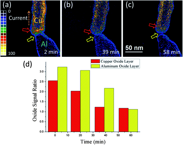 |
| | Fig. 2 (a)–(c) Sequence of EFTEM images of oxygen. The applied bias was 2 V from Al to Cu. The energy width was set to be 10 eV with a center at 532 eV for oxygen. The exposure time range of all the mappings was fixed at 10 s. The red and yellow arrows indicate the sampling region of mean signal density of oxygen on the top of each nanorod. The scale bar for (a)–(f) is 50 nm. (d) Histogram of oxide signal ratio at different times. The Y axis indicates the ratio of the mean signal density of oxygen for the top sampling region and body region. Oxygen signal at the interface decreased significantly under electrical loadings. Therefore, the two nanorods demonstrated a significant decrease of oxygen atoms at the interface. | |
2. Electromigration
Fig. 3 shows that the applied electrical loadings dominated the electromigration of Cu atoms in the contact region. Throughout the experiment, a negative bias of 3 V was subjected to the Cu side (the electron current flowed from Cu to Al). The ohmic contact was accomplished after 25 min constant bias (the current density was about 9 × 10⁷ A m−2 at that point). Fig. 3(a)–(c) show the Cu maps of the contact region. The energy width was set to be 30 eV with center at 931 eV for Cu. The exposure time range of all the mappings was fixed at 30 s. Fig. 3(d)–(f) show the TEM images corresponding to the above EFTEM maps. The contact area of the bonding region is approximately 1962.5 nm2. The red dashed lines in Fig. 3(a)–(c) indicate the electromigration induced growth of the Cu nanorod. Initially, the migration was restricted before the formation of ohmic contact, as shown in Fig. 3(a). After the removal of the surface oxide layer and the formation of ohmic contact, the electromigration became activated (Fig. 3(b) and (c)). Eventually, the Al nanorod melted prior to the Cu nanorod at 68 min (the current density was about 2.5 × 10⁹ A m−2 before melting). Typically, the diffusion and electromigration of Al is strongly influenced by grain boundaries, while the electromigration of Cu is dominated by surface diffusion.20 According to Blech's work, the electromigration process is governed by the following formula:22| | 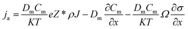 | (1) |
where ja is the density of atoms' flow, e is the charge of the electron, Z* is the effective charge of the metal, ρ is the resistivity of the metal, J is the current density, K is the Boltzmann constant, T is the absolute temperature of the contact region, σ is the static stress, Ω is the atomic volume and Dm and Cm are the coefficient of diffusion, and the number of atoms per unit volume of metal material, respectively. In the assumption of hydrostatic stress mode, the thermal diffusion term for metal atoms is smaller than the electromigration term and the stress term.20,23 As described in eqn (1), electromigration usually accompanies with stress concentration, which is generally induced by the formation of negative composition gradients, i.e., more atoms concentrate on the top of the nanorod.22 When more Al atoms migrate to the Cu nanorod, the gradient of atomic concentration becomes more significant, leading to bigger stress accumulation (see ESI Fig. 3*†). Since the current density was very small before the formation of ohmic contact (Fig. 3(a)), the electromigration was significantly less apparent compared with the cases in which ohmic contacts were formed (Fig. 3(b) and (c)). The effective charge numbers Z* are −30 and −5 for Al and Cu, respectively.21,24 For self-diffusion, the constants of intrinsic diffusivity are 2.3 × 10⁻⁴ cm2 s−1 and 7.8 × 10⁻⁵ cm2 s−1 for Al and Cu, respectively. However, their effective diffusivities will turn to 4.2 × 10⁻¹⁴ cm2 s−1 and 4.2 × 10⁻¹⁹ cm2 s−1 at 773 K. Therefore, considering the great differences in (DmZ*) at different temperatures, Al presents a more intensive electromigration behavior than Cu does under the same electrical loading.20
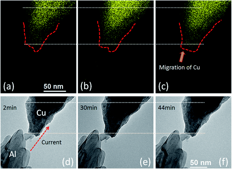 |
| | Fig. 3 (a)–(c) Sequence of EFTEM images. The energy width was set to be 30 eV with the center at 931 eV for Cu. The exposure time range of all the mappings was fixed at 30 s. The applied bias was 3 V from Al to Cu. The white dashed lines are drawn as references, and the red dashed lines indicate the electromigration of Cu atoms on the basis of the profile of the Cu signal. (d)–(f) Sequence of TEM images corresponding to the above images. The scale bars for (a)–(f) are 50 nm. | |
3. Electromigration-dominated cutting process
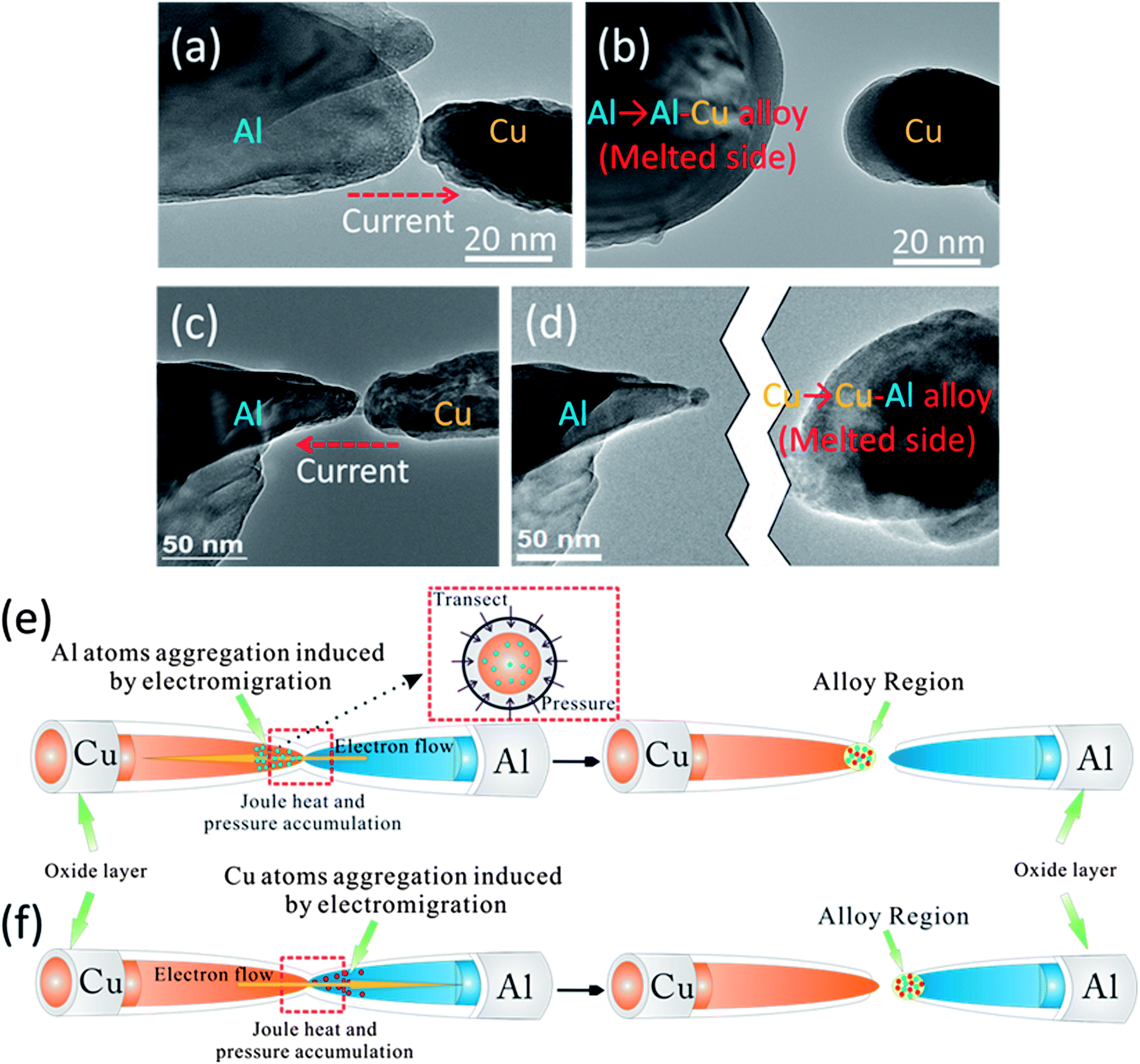
The melting points for Cu and Al bulk materials are 1357 and 933.4 K, respectively. Al should melt away regardless of the direction of bias. However, real-time high resolution TEM images show that when the current flowed from Al to Cu (negative bias, Fig. 4(a)), the Al nanorods melted prior to the Cu nanorods (Fig. 4(b)); when the current flowed from Cu to Al (positive bias, Fig. 4(c)), the Cu nanorods melted prior to the Al nanorods (Fig. 4(d)). Several factors might affect this cutting process. Size effects and compressive pressure could induce variation of the melting point of nanomaterials.3,4,25 According to the Gibbs–Thomson formula (T(d) = T(∞) − 4T(∞)σsl/Hfρsd),26 it is assumed that the melting point of nanomaterials decreasing with the decrease of size is caused by the increase of surface energy. For the specific sample with a diameter of 40 nm, the decrease of melting point is only 19.62 and 22.23 K for Al and Cu, respectively. Although the latent heat of fusion Hf will decrease with decreasing size, the change is less than 20% for nanostructures with a diameter larger than 15 nm.26 Thus, the size effects can't be the main reason for this phenomenon.
 |
| | Fig. 4 (a) TEM images of Al and Cu nanorods before the bias was applied. (b) TEM image of two nanorods after melting, the bias was 2 V from Al to Cu. The scale bars for (a) and (b) are 20 nm. (c) TEM image of Al and Cu nanorods before the bias was applied. (d) TEM image of two nanorods after melting, the bias was 2 V from Cu to Al. The scale bars for (c) and (d) are 50 nm. (e) and (f) are schemes of the electromigration-dominated cutting process corresponding to above images. The alloy region was formed on different nanorod positions because of the different electromigration directions. | |
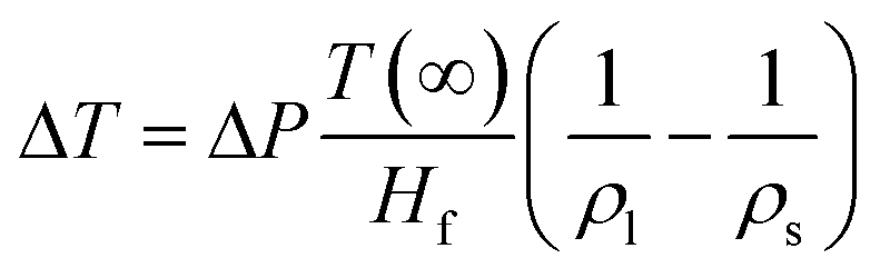
Accumulated pressure caused by thermal expansion increased the melting points. The increase of melting point is described by:
| |  | (2) |
where Δ
T is the increase of melting point, Δ
P is the accumulated pressure,
T(∞) is the melting point of bulk materials,
Hf is the latent heat of fusion, and
ρl and
ρs are the densities of liquid and solid metals, respectively. Typically, metal possesses higher coefficients of thermal expansion than metal oxide. Accumulated pressure was mainly caused by the difference of coefficient of thermal expansion between metal and metal oxide, which is 5.3 × 10
−5 K
−1 for Al and 3.4 × 10
−5 K
−1 for Cu.
28 The thermal expansion induced pressure can be described by:
| | | ΔP = KB(T(∞) − Troom)(αmetal − αoxide) − P*oxide | (3) |
where
KB is the bulk modulus of the metal,
Troom is the room temperature,
P*oxide is the pressure induced by buckling of the metal oxide shell, and
αmetal and
αoxide are the coefficient of the thermal expansion of metal and metal oxide, respectively. To counteract the difference of melting point (401.6 K) between Al and Cu, the accumulated pressure generated on the Al nanorod should be as high as 3.305 GPa even without considering the buckling of metal oxide shell (simply treat oxide shell as rigid body). Moreover, although the injected metal atoms may cause expansive stress against the oxide shell on the cathode nanorod, however, the metal atoms on the cathode would migrate to the body region (as Fig. 4* in ESI
†) and greatly reduce the effect because both Cu and Al have the same direction of electromigration. Considering the buckling of covered oxide shells and the decrease of hardness induced by accumulated Joule heating, we denote that such high pressure cannot be enabled merely by thermal expansion. Although accumulated pressure is not the dominant mechanism for this phenomenon, this pressure still facilitated the breakdown process when the interface area had a great decrease on yielding stress as the temperature was near its melting point.
33
Aside from the above mentioned size and thermal expansion effects, electromigration should be the main reason for this phenomenon. To better understand the domination of electromigration on cutting positions, a statistical scheme of cutting positions for nanorods with different contact areas is illustrated in Fig. 5. The statistical results directly demonstrate the dependence of melting results on the direction of bias. The findings prove the independence of melting position on the contact area, which indicates a weak influence of size effect. Moreover, the region where cutting occurred turned out to be the area in which the alloy formed (see ESI Fig. 4*†). According to the phase diagram of the Cu–Al bulk material system, only 17.5% (atomic percent) of Cu can cause the melting point of the alloy to drop to the lowest point of 821.2 K, whereas over 40% of Al can cause the melting point of the alloy to become lower than Al melting point.27 Given that the properties of nanometals are size dependent, the phase diagram should also be size dependent.28,29 Although no computational or experimental data exist regarding the nano-phase-diagram of the binary Al–Cu system, according to diverse computational results of other metal materials, the temperature of solidus and liquidus would drop and the tendency of curves do not significantly change for a particle size larger than 15 nm.28–32 In our case, the diameters of most nanorods are more than 15 nm and the nanorods are covered by an oxide layer which greatly reduces the surface effects.30 Hence, the tendency of the phase diagram should not deviate much from that of bulk materials'. As stated before, Al demonstrated a more intensive electromigration behavior than Cu did, especially under high temperature (such as the contact region of nanorods under electrical loadings). Therefore, the following explanation could be drawn from that abnormal melting phenomenon. (I) When positive bias (Cu to Al) was applied, a large amount of Al atoms migrated to the Cu nanorod and formed an alloy region on it. This migration resulted in the significant decrease of the melting point of the alloy region, thereby causing the melting of the alloy region prior to the Al nanorod (Fig. 4(e)). (II) When negative bias (Al to Cu) was applied, comparatively minimum Cu atoms migrated to the Al nanorod and formed an alloy region on it. This minimum amount of migration caused a decrease in the melting point of the alloy region and consequently the melting of the alloy region before the Cu nanorod (Fig. 4(f)). Therefore, with this electromigration dominant mechanism, we can conduct controllable cutting for nanometals with positive or negative effective charge (Z*) by modulating the direction of the applied bias.
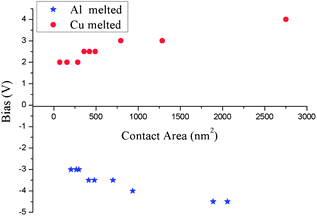 |
| | Fig. 5 Statistical scheme of the dependence of melting results on the direction of bias and contact area. The positive bias is defined as the current flowing from Cu to Al whereas negative bias is defined as the current flowing from Al to Cu. | |
Conclusion
In summary, we successfully carried out the dynamic observation of nanoscale interface atom migration and electromigration-dominated cutting process within a Cu–Al heterostructure nanojoining system. The oxygen atom migration at the contact interface was proven to be a thermal dominated process. The electromigration process became dominant only after the migration of oxygen atoms and the complication of ohmic contact. Nanometal electromigration and cutting behavior could be modulated by the direction of external electrical loadings. These experiments demonstrate the applicability of electrical methods to modulate the electromigration, composition and properties of nanometals. This concept offers an insight of a potential failure mechanism for interconnects of the nanodevice. This concept may also be valuable for the nanoscale fabrication of widely used metal materials as interconnects and intermetallic compounds.
Acknowledgements
This work was founded from Ministry of Education of China, National Natural Science Foundation of China (no. 51071044, 51201032) and Jiangsu Province Funds (no. BK2012024, BK2011592). The authors would like to acknowledge the support by General Motors global R&D and FEI Company.
Notes and references
- Y. Xiong, Z. Liu and X. Zhang, Appl. Phys. Lett., 2009, 94, 203108 CrossRef.
- Y. Li, F. Liu, L. Xiao, K. Cui, X. Feng, W. Zhang and Y. Huang, Appl. Phys. Lett., 2013, 102, 063113 CrossRef.
- O. A. Yeshchenko, I. M. Dmitruk, A. A. Alexeenko and A. M. Dmytruk, Phys. Rev. B: Condens. Matter Mater. Phys., 2007, 75, 085434 CrossRef.
- T. Castro, R. Reifenberger, E. Choi and R. P. Andres, Phys. Rev. B: Condens. Matter, 1990, 42, 8548–8556 CrossRef CAS.
- B. Wunderle and B. Michel, Microelectron. Reliab., 2006, 46, 1685–1694 CrossRef PubMed.
- M. D. Uchic, D. M. Dimiduk, J. N. Florando and W. D. Nix, Science, 2004, 305, 986–989 CrossRef CAS PubMed.
- J. Schiøtz and K. W. Jacobsen, Science, 2003, 301, 1357–1359 CrossRef PubMed.
- Z. Shan, E. A. Stach, J. M. K. Wiezorek, J. A. Knapp, D. M. Follstaedt and S. X. Mao, Science, 2004, 305, 654–657 CrossRef CAS PubMed.
- J. R. Greer, J. Th and M. De Hosson, Prog. Mater. Sci., 2011, 55, 654–724 CrossRef PubMed.
- T. Ishida, K. Kakushima, N. Sasaki and H. Fujita, Nanotechnology, 2010, 21, 435705 CrossRef PubMed.
- C. Huang, C. Hsin, C. Wang, F. Chu, C. Kao, J. Chen, Y. Huang, K. Lu, W. Wu and L. Chen, Nanoscale, 2012, 4, 4702–4706 RSC.
- Y. Lu, J. Huang, C. Wang, S. Sun and J. Lou, Nat. Nanotechnol., 2010, 5, 218–224 CrossRef CAS PubMed.
- D. Kiener, P. Hosemann, S. A. Maloy and A. M. Minor, Nat. Mater., 2011, 10, 608–613 CrossRef CAS PubMed.
- Q. Yu, Z. Shan, J. Li, X. Huang, L. Xiao, J. Sun and E. Ma, Nature, 2010, 463, 335–338 CrossRef CAS PubMed.
- A. Misra and C. Daraio, Adv. Mater., 2009, 21, 2305–2308 CrossRef CAS.
- H. Tohmyoh, J. Appl. Phys., 2009, 105, 014907 CrossRef.
- H. Tohmyoh and S. Fukui, J. Nanopart. Res., 2012, 14, 1116–1124 CrossRef.
-
D. B. Williams and C. B. Carter, in Transmission Electron Microscopy—A Textbook for Materials Science, Plenum, New York, 1996, vol. 4, pp. 721–728 Search PubMed.
-
R. F. Egerton, in Electron Energy-Loss Spectroscopy in the Electron Microscope, Springer Science+Business Media, New York, 3rd edn, 2011, pp. 98–108 Search PubMed.
- K. N. Tu, J. Appl. Phys., 2003, 94, 5451–5473 CrossRef CAS.
- V. T. Srikar and C. V. Thompson, Appl. Phys. Lett., 1999, 74, 37–39 CrossRef CAS.
- I. A. Blech, J. Appl. Phys., 1976, 48, 473–477 CrossRef.
- J. R. Lloyd and J. J. Clement, Appl. Phys. Lett., 1996, 69, 2486–2488 CrossRef CAS.
- A. S. Oates, E. P. Martin, D. Alugbin and F. Nkansah, Appl. Phys. Lett., 1993, 62, 3273–3275 CrossRef CAS.
- Q. Shu, Y. Yang, Y. Zhai, D. Y. Sun, H. J. Xiang and X. G. Gong, Nanoscale, 2012, 4, 6307–6311 RSC.
- J. Sun and S. L. Simon, Thermochim. Acta, 2007, 463, 32–40 CrossRef CAS PubMed.
-
E. A. Brandes and G. B. Brook, in Smithells Metals Reference Book, Bath Press, 7th edn, 1998, pp. 11–35 Search PubMed.
- G. Garzel, J. Janczak-Rusch and L. Zabdyr, Comput. Coupling Phase Diagrams Thermochem., 2012, 32, 53–56 Search PubMed.
- T. Ivas, A. N. Grundy, E. P. Karadeniz and L. J. Gauckler, CALPHAD: Comput. Coupling Phase Diagrams Thermochem., 2012, 36, 57–64 CrossRef CAS PubMed.
- E. A. Sutter and P. W. Sutter, ACS Nano, 2010, 4, 4943–4947 CrossRef CAS PubMed.
- J. Lee, J. Lee, T. Tanaka and H. Mori, Nanotechnology, 2009, 20, 475706 CrossRef PubMed.
- L. H. Liang, D. Liu and Q. Jiang, Nanotechnology, 2003, 14, 438–442 CrossRef CAS.
- J. Zhao, H. Sun, S. Dai, Y. Wang and J. Zhu, Nano Lett., 2011, 11, 4647–4651 CrossRef CAS PubMed.
Footnote |
| † Electronic supplementary information (ESI) available: Discussion of electron beam irradiation and electrical measurements during nanojoining process and proof of the electromigration induced stress concentration phenomenon. See DOI: 10.1039/c3nr03911k |
|
| This journal is © The Royal Society of Chemistry 2014 |
Click here to see how this site uses Cookies. View our privacy policy here.