Random telegraph noise and resistance switching analysis of oxide based resistive memory†
Shinhyun
Choi
,
Yuchao
Yang
and
Wei
Lu
*
Department of Electrical Engineering and Computer Science, University of Michigan, MI 48109, USA. E-mail: wluee@eecs.umich.edu
First published on 17th October 2013
Abstract
Resistive random access memory (RRAM) devices (e.g. “memristors”) are widely believed to be a promising candidate for future memory and logic applications. Although excellent performance has been reported, the nature of resistance switching is still under extensive debate. In this study, we perform systematic investigation of the resistance switching mechanism in a TaOx based RRAM through detailed noise analysis, and show that the resistance switching from high-resistance to low-resistance is accompanied by a semiconductor-to-metal transition mediated by the accumulation of oxygen-vacancies in the conduction path. Specifically, pronounced random-telegraph noise (RTN) with values up to 25% was observed in the device high-resistance state (HRS) but not in the low-resistance state (LRS). Through time-domain and temperature dependent analysis, we show that the RTN effect shares the same origin as the resistive switching effects, and both can be traced to the (re)distribution of oxygen vacancies (VOs). From noise and transport analysis we further obtained the density of states and average distance of the VOs at different resistance states, and developed a unified model to explain the conduction in both the HRS and the LRS and account for the resistance switching effects in these devices. Significantly, it was found that even though the conduction channel area is larger in the HRS, during resistive switching a localized region gains significantly higher VO and dominates the conduction process. These findings reveal the complex dynamics involved during resistive switching and will help guide continued optimization in the design and operation of this important emerging device class.
RRAM has been widely viewed as a promising candidate for future data storage applications. Previous studies on oxide-based RRAM have reported endurance up to 1012,1,2 subnanosecond switching3 and device size scaling down to 10 nm.4 However, important questions regarding the nature of the conduction channels and the switching dynamics still remain under debate. Direct observation of the conduction channels formed by oxygen vacancy (VO) redistribution is challenging, and electrical characterizations only provide limited information. Here, we report detailed analysis on the RTN noise of the RRAM devices. When combined with transport studies the results lead to a unified picture of the resistive switching process and provide valuable information regarding the nature of the conduction channels.
The resistive memory devices studied here are based on a Pd/TaOx/Ta2O5/Pd structure, in which the Ta2O5 layer acts as the switching layer and the TaOx layer acts as the base layer that controls the device on-state resistance and provides needed oxygen vacancies for resistive switching.1,5 The devices were fabricated on a Si/SiO2 substrate with a 100 nm thermal SiO2 layer. The bottom electrode consisting of 5 nm thick NiCr and 35 nm-thick Pd was first patterned by e-beam lithography and deposited by e-beam evaporation. The TaOx base layer (∼50 nm, 2.5 × 10⁻⁴ Ω cm) was deposited by direct current (DC) reactive sputtering of a Ta metal target with an Ar/O2 (3% oxygen partial pressure) gas mixture at 400 °C, followed by the Ta2O5 switching layer (∼5 nm) deposition by radio frequency (RF) sputtering of a Ta2O5 ceramic target at room temperature. Finally, the top-electrode consisting of 30 nm thick Pd and 20 nm thick Au was patterned by e-beam lithography and deposited by the e-beam evaporation, forming a crossbar structure with the bottom electrode. Devices with different sizes from 50 nm × 50 nm to 5 μm × 5 μm were fabricated and tested, as shown in the inset of Fig 1(a). During testing, the bias voltage was applied to the top electrode with the bottom electrode grounded. Reliable bipolar resistance switching characteristics with current–voltage (I–V) curves as shown in Fig. 1(a) were obtained after an electroforming process with up to −6 V. The electrical characterizations and noise measurements were performed using a custom-built measurement system and a temperature-variable probe station (Desert Cryogenics TTP4).
 | ||
| Fig. 1 (a) I–V characteristics of a typical device showing the bipolar switching effects. Inset: SEM image of the device. Scale bar is 5 μm. (b) Current–time plots measured at 0.1 V for the LRS and HRS, respectively. Insets: zoomed-in plots of the circled areas for the LRS (left) and HRS (right), showing pronounced RTN in the HRS. | ||
A typical device switches to the LRS at around −0.7 V and switches back to the HRS at around 1.2 V (Fig. 1(a)). Noise measurements were performed by monitoring the device current under a low, constant bias voltage of 0.1 V (Fig. 1(b)). Significantly, in the HRS, abrupt current jumps between two (or more) discrete current levels can be regularly observed (Fig. 1(b), right inset), corresponding to significant RTN. On the other hand, RTN was not observed in the LRS despite the fact that the resistance values between the LRS and the HRS differ by only ∼10. Out of more than 70 devices tested, all devices showed similar behaviors.
Statistical and temperature dependent studies were carried out to reveal the nature of the observed RTN behaviors in the HRS. The RTN data recorded in time-domain from a 500 nm × 500 nm cell in the HRS is shown in Fig. 2(a) (red line). Current jumps of ∼10% between two discrete states are clearly observed. Plotting the current readings vs. occurrence clearly reveals a bimodal resistance distribution corresponding to two metastable states, as shown in Fig. 2(b). RTN as large as 25% has been observed in these devices in the HRS. Such high noise levels can have a significant impact on device operation and deserve careful analysis. To analyze the RTN signal, a custom MATLAB code was used to capture the current jumps and measure the dwell time at each state.6 The algorithm tests 2 hypotheses (whether a switching event happens or not) within a given time window and maximizes the probability of both hypotheses in the presence of white noise. Using the maximum likelihood estimates, one can judge if a switching event occurs or not by examining the difference between the 2 maximized likelihood values and comparing it to a pre-set threshold value. If a switching event is judged to have occurred, the switching time is also recorded as the time that leads to the maximum likelihood. The reliability of this algorithm is verified in Fig. 2(a), where every current jump was successfully captured by the code (gray line) with no false positive or negative alarms. The time the device spent in each state is then recorded and analyzed, the histograms of which are plotted in Fig. 2(c) and (d). For both metastable current states, the dwell time distribution can be fitted well with a Poisson distribution (solid lines). Following standard statistics, the Poisson distribution describes stochastic events such that the probability that an event (current jump) occurs within Δt at a given time t is7,8
 | (1) |
 | ||
| Fig. 2 (a) Time-domain analysis of the RTN behavior showing raw data (red) and reproduced data (grey) based on the capture program. (b) Histograms of current vs. occurrence showing a bimodal distribution corresponding to the two current levels causing RTN. (c and d) Histograms of the dwell times in the upper (c) and lower (d) current levels. The red lines are Poisson fits using τ as the only fitting parameter. | ||
Following the discussions in ref. 9, the RTN in the RRAM can be explained as follows: when an electron falls into a trap near the conduction path in the RRAM device, it depletes the conduction path and causes the current to change to a lower level, as illustrated in Fig. 3(b). Similarly, the current will change to a higher level when the trapped electron is detrapped. Since the trapping/detrapping events are thermally activated and stochastic in nature, these processes lead to the stochastic jumps between the current levels and the observed Poisson distribution of dwell times with well-defined characteristic time constants, if the current is affected by one dominant trap.
 | ||
| Fig. 3 (a) Temperature dependence of the characteristic dwell times in the upper and lower current levels. The lines are fits following the Arrhenius equation. (b) Schematic of the cause for RTN. The trapping and detrapping of a trap site near the channel lead to jumps in discrete current levels. The dashed circle represents the area that may be electrostatically depleted by the trapped electron. (c and d) Histograms and fits of the dwell times at the upper current levels at 250 K and 300 K, respectively. | ||
More evidence supporting this theory can be obtained from temperature dependent studies. Briefly, time-domain RTN data were analyzed at different temperatures and the extracted characteristic dwell time, τ, was then plotted as a function of temperature (T), as shown in Fig. 3(a). Typical results obtained at 250 K and 300 K are shown in Fig. 3(c) and (d). Both τup and τdown, corresponding respectively to the characteristic time constants in the upper current (detrapped) level and lower current (trapped) level, were recorded and analyzed. It can be seen that both time constants increase as the temperature is decreased.8,12,13 Fitting the τ–T curves using an Arrhenius-type relationship produces the activation energies for the electron trapping and detrapping processes, which are 0.16 eV for electron trapping and 0.34 eV for electron detrapping for the device as shown in Fig. 3. The schematic of the trapping/detrapping processes that lead to RTN is shown in Fig. 3(b).
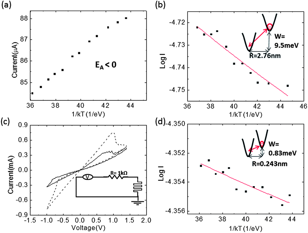
It is interesting to note that RTN in general is not observed in the LRS, even though the resistance values between the LRS and HRS do not seem to differ significantly. We believe the different noise behaviors in the HRS and LRS can shed light into the mechanism behind resistive switching in these RRAM devices, and the evolution of the noise characteristics correlates with the evolution of the conduction channels. In metal oxide based devices the conduction is believed to be through conduction channels formed in regions with higher concentration of VOs. Changes in VO distribution lead to changes in resistance states, with the LRS having a higher VO concentration in the conduction channels compared with the HRS.1,2,5,14 Consequently, these changes in trap distributions can also lead to different noise characteristics. To verify this hypothesis, temperature dependent studies of conduction through the LRS and HRS were carried out, as shown in Fig. 4(a) and (b). In the LRS, the current decreases as the temperature is increased, suggesting that the conduction channel is metallic with a negative activation energy for electron transport. On the other hand, in the HRS the device current increases as the temperature is increased, suggesting that the conduction channel is semiconducting with a positive activation energy for electron transport.
 | ||
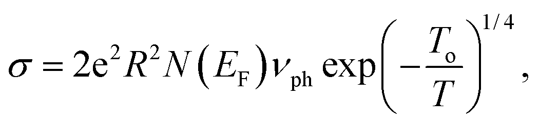
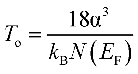
| Fig. 4 (a) Temperature dependence of electron transport in the LRS. (b) Temperature dependence of electron transport in the HRS. Inset: schematic of the hopping process. (c) Solid line: I–V characteristics without the series resistor, showing switching between the HRS and the LRS; dashed line: I–V characteristics with a 1 kΩ series resistor. The device is programmed to an intermediate state instead. Inset: the circuit schematic. (d) Temperature dependence of electron transport in the intermediate state. Inset: hopping with more closely spaced trap sites and lower hopping energy in the intermediate state compared to the HRS. | ||
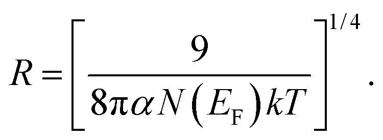
In the HRS, the electron transport is believed to be facilitated by electron hopping mediated through the VO trap sites,15 and the conduction can be explained using the variable-range hopping (VRH) model. If we define 1/α as the decay length of the electron wavefunction and R as the average hopping distance, then the electron can hop to another trap site within the decay length if αR is equal to or less than unity, as shown in the inset of Fig. 4(b). During the process, the electron overcomes the hopping energy barrier, W, which corresponds to the energy difference between the two trap sites, assisted by thermal energy. As a result, the conductivity can be written at a low electrical field as16
 | (2) |
 | (3) |
Plugging eqn (3) into eqn (2), the most probable conduction occurs when
 | (4) |
 | (5) |
 . We note that eqn (5) is the well-known Mott equation for transport through disordered systems in three-dimension.
The temperature dependent results shown in Fig. 4(b) can be well-fitted with eqn (5), which leads to an extracted density of localized (oxygen vacancy) trap states N(EF) of 1.2 × 10²¹ eV−1 cm−3, average hopping distance R of 2.8 nm and activation energy at room temperature W of 9.5 meV for the HRS. Here we assumed the decay length α to be 0.2 nm−1, a value commonly used for disordered films.17–19 The R and W values obtained here are consistent with the constraints for VRH conduction that αR is equal to or less than unity and the hopping energy barrier is smaller than thermal energy. If otherwise the localization is strong enough (i.e. αR is larger than unity), the nearest-neighbor hopping (NNH) process should be employed instead.16,18
The evolution of the conduction channels can be analyzed by studying how the distribution of VOs evolves as the device is programmed from the HRS to an intermediate state then eventually to the LRS. To create the intermediate state, a 1 kΩ series resistor was attached in front of the device during programming, as shown in the inset of Fig. 4(c). During programming the series resistor creates a voltage divider effect that slows down the filament growth as the RRAM resistance is reduced.7,20–22 As a result, an intermediate state between the HRS and the fully programmed LRS can be obtained. The series resistor was not used when programming to the fully on LRS or when resetting to the HRS. The intermediate state shows similar temperature dependence to the HRS, as shown in Fig. 4(d). Following the same treatment as the HRS, a density of localized (VO) state of 2.0 × 1025 eV−1 cm−3, average hopping distance of 0.24 nm and hopping energy of 0.83 meV can be obtained. The significantly increased density of states for VO and reduction of the hopping distance between VO sites are consistent with the oxygen-vacancy mediated resistive switching model: as the device state changes from HRS to LRS, more oxygen vacancies are accumulated in the conduction channel region and the distance between oxygen vacancies is significantly reduced with increased density of localized VO states which in turn leads to a decrease in device resistance. These processes are schematically shown in Fig. 5(a) and (b).
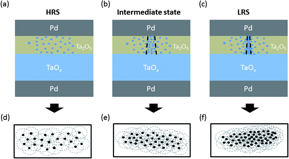 | ||
| Fig. 5 Schematics showing the changes in VO distribution for the HRS, the intermediate state and the LRS in the Ta2O5 switching layer, respectively. The dashed lines in (b) and (c) highlight the filament region with higher VO concentration than the rest of the film. (d–f) Corresponding changes in the overlap of electron wavefunctions lead to different resistance values for the HRS, intermediate state and LRS. Dots: localized states, gray dashed circle: the localization radii. | ||
Based on noise and transport analyses, a unified picture of the resistive switching behavior can be obtained. Even in the HRS, the conduction through the device is not homogeneous but rather dominated by “channels” with higher VO concentration than the rest of the matrix, as shown in Fig. 5(a). Conduction through the channels is by electron hopping mediated by the VO traps. While many VO trap sites are distributed close to an average hopping distance of ∼2 nm and form the conduction channel, the broad VO distribution in the film means that there will unavoidably be some VO trap sites with a distance much larger than the rest. These VO traps are too far from the channel to contribute to conduction current, and will rather act as a noise source as they occasionally trap and detrap electrons, as shown in Fig. 5(a). As a result, the RTN effect will be pronounced if only one or a few discrete VOs are within the appropriate distance from the channel (too far the effect becomes very week while too close the traps become part of the channel itself10). These conditions are satisfied in the HRS when the VO concentration is still not too high. This hypothesis also explains the observation that the RTN noise can vary significantly after each set and reset process even if the device is reset to the same resistance value (see the ESI, Fig. S1†), since the distribution of VOs will be different after each set and reset process.
We now turn to the switching process from the HRS to the LRS. During this set process, more VOs are accumulated in the conduction channel and the distance between the VO sites becomes significantly reduced (as evidenced by the reduction of average VO spacing from ∼2 nm in the HRS to ∼0.24 nm in the intermediate state)23 and eventually extended electron states are formed when the electron wavefunctions overlap sufficiently, as shown in Fig. 5(f). This leads to the formation of the metallic LRS and the observed negative temperature coefficients. Significantly, our analysis also suggests that the formation of LRS conduction channels is not uniform but rather a localized effect. Estimations of the effective channel size from the calculated conductivity using eqn (5) and the measured conductance values resulted in a channel diameter of 42 nm for the HRS and only 3 nm for the intermediate state. Here we assumed a νph value of 1012 s−1 (ref. 16) and channel length of 5 nm which corresponds to the deposited Ta2O5 film thickness. What is interesting is that the channel (conduction filament) diameter for the intermediate state is much smaller than that of the HRS, even though during resistance switching more VOs are injected into the Ta2O5 layer. This result clearly suggests that the conducting channel (filament) formation is a localized process, as non-uniformities in the VO distribution in the film lead to a few local “hot spots” that attract higher concentration of VOs than the rest of the film. The enhanced local conductivity likely leads to higher local temperature which further speeds filament growth at these locations.
This filament formation picture is schematically illustrated in Fig. 5(a)–(c), which show the evolutions of oxygen vacancy distribution from the HRS through the intermediate state and to the LRS, while Fig. 5(d–f) show how the conduction evolves from VRH to the formation of extended states. The lack of RTN in the LRS can now be readily explained by the fact that there are simply too many VO trapping sites whose noise effects overlap, making effects from individual trap site (RTN) noise impossible to resolve, i.e. similar to the observation of the transition from RTN to regular 1/f noise in silicon inversion layers as the device size increases.10
In summary, we found that significant RTN exists in the HRS of the RRAM device. Systematic analysis of the RTN and electrical transport through the RRAM device verified that the conduction channel formation is associated with the (re)distribution of VOs. While in the HRS the discrete VOs outside the channel region can lead to significant RTN up to 25%, in the LRS the higher VO concentration causes the individual effects to overlap and the disappearance of RTN effects. Modeling of the transport data also leads to insight into the spacing of the VO sites and the effective filament size. Specifically, as the device is switched from HRS to LRS, the conduction channel area is actually reduced with a much higher VO density obtained locally. These findings will provide valuable information on the application and design of oxide-based resistive switching devices for memory and logic applications.
Acknowledgements
The authors thank J. Lee, L. Chen and P. Sheridan for useful discussions. This work was supported in part by the National Science Foundation (NSF) (ECCS-0954621), and by the AFOSR through MURI grant FA9550-12-1-0038 and grant FA9550-12-1-0441. S.H. Choi is supported in part by the Samsung Scholarship. This work used the Lurie Nanofabrication Facility at the University of Michigan, a member of the National Nanotechnology Infrastructure.References
- M.-J. Lee, C. B. Lee, D. Lee, S. R. Lee, M. Chang, J. H. Hur, Y.-B. Kim, C.-J. Kim, D. H. Seo, S. Seo, U.-I. Chung, I.-K. Yoo and K. Kim, Nat. Mater., 2011, 10, 625–630 CrossRef CAS PubMed.
- J.-J. Yang, M.-X. Zhang, J. P. Strachan, F. Miao, M. D. Pickett, R. D. Kelley, G. Mederos-Ribeiro and R. S. Williams, Appl. Phys. Lett., 2010, 97, 232102 CrossRef.
- A. C. Torrezan, J. P. Strachan, G. Medeiros-Ribeiro and R. S. Williams, Nanotechnology, 2011, 22, 485203 CrossRef PubMed.
- B. Govoreanu, G. Kar, Y. Chen, V. Paraschiv, S. Kubicek, A. Fantini, I. Radu, L. Goux, S. Clima and R. Degraeve, et al., Electron Devices Meeting (IEDM), IEEE International, 2011, pp. 31–36 Search PubMed.
- Y. Yang, P. Sheridan and W. Lu, Appl. Phys. Lett., 2012, 100, 203112 CrossRef.
- W. Lu, Z. Ji, L. Pfeiffer, K. W. West and A. J. Rimberg, Nature, 2003, 423, 422–425 CrossRef CAS PubMed.
- S. H. Jo, K.-H. Kim and W. Lu, Nano Lett., 2009, 9(2), 870–874 CrossRef CAS PubMed.
- R. Soni, P. Meuffels, A. Petraru, M. Weides, C. Kugeler, R. Waser and H. Kohlstedt, J. Appl. Phys., 2010, 107, 024517 CrossRef.
- D. Ielmini, F. Nardi and C. Cagli, Appl. Phys. Lett., 2010, 96, 053503 CrossRef.
- K. S. Ralls, W. J. Skocpol, L. D. Jackel, R. E. Howard, L. A. Fetter, R. W. Epworth and D. M. Tennant, Phys. Rev. Lett., 1984, 52, 228–231 CrossRef CAS.
- H. D. Xiong, W. Wang, Q. Li, C. A. Richter, J. S. Suehle, W. K. Hong, T. Lee and D. M. Fleetwood, Appl. Phys. Lett., 2007, 91, 053107 CrossRef.
- Y. H. Tseng, W. C. Shen and C. J. Lin, J. Appl. Phys., 2012, 111, 73701–737015 CrossRef PubMed.
- J.-K. Lee, J.-W. Lee, J. Park, S.-W. Chung, J. S. Roh, S.-J. Hong, I.-W. Cho, H.-I. Kwon and J.-H. Lee, Appl. Phys. Lett., 2011, 98, 143502 CrossRef.
- J. J. Yang, D. B. Strukov and D. R. Stewart, Nat. Nanotechnol., 2012, 8(1), 13–24 CrossRef PubMed.
- S. Yu, X. Guan and H.-S. P. Wong, Appl. Phys. Lett., 2011, 99, 063507 CrossRef.
- N. Mott and E. Davis, Electronic Processes in Non-crystalline Materials, Clarendon press, Oxford, 1979 Search PubMed.
- Z. H. Khani, M. M. Malik, M. Zulfequar and M. Husain, J. Phys.: Condens. Matter, 1995, 4, 8979 CrossRef.
- I. Goldfarb, F. Miao, J. J. Yang, W. Yi, J. P. Strachan, M.-X. Zhang, M. D. Pickett, G. Medeiros-Ribeiro and R. S. Williams, Appl. Phys. A: Mater. Sci. Process., 2012, 107, 1–11 CrossRef CAS.
- M. Brodsky and R. Gambino, J. Non-Cryst. Solids, 1972, 810, 739–744 CrossRef.
- A. Fantini, D. Wouters, R. Degraeve, L. Goux, L. Pantisano, G. Kar, Y. Y. Chen, B. Govoreanu, J. Kittl and L. Altimime, et al., Memory Workshop (IMW), 4th IEEE International, 2012, pp. 1–4 Search PubMed.
- S. H. Jo and W. Lu, Nano Lett., 2008, 8(2), 392–397 CrossRef CAS PubMed.
- K. H. Kim, S. H. Jo, S. Gaba and W. Lu, Appl. Phys. Lett., 2010, 96, 053106 CrossRef.
- F. R. Allen and C. J. Adkins, Philos. Mag., 1972, 26, 1027–1042 CrossRef CAS.
Footnote |
| † Electronic supplementary information (ESI) available. See DOI: 10.1039/c3nr05016e |
| This journal is © The Royal Society of Chemistry 2014 |